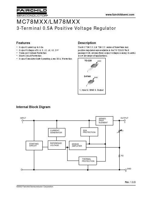
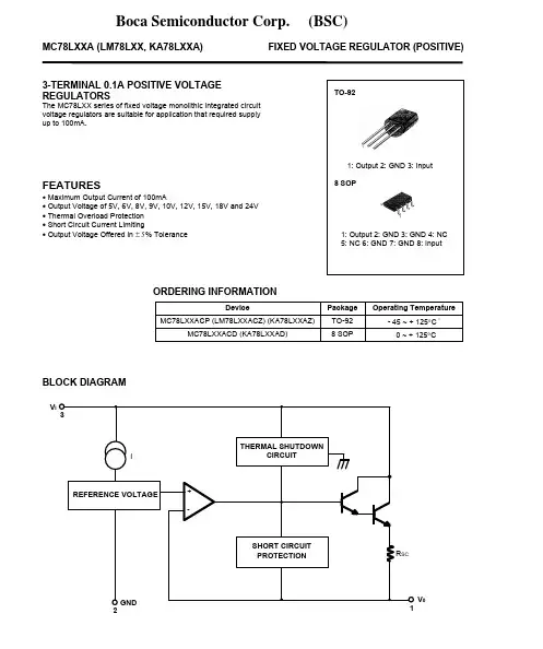
MC78M00, MC78M00A Series500 mA Positive Voltage RegulatorsThe MC78M00/MC78M00A Series positive voltage regulators are identical to the popular MC7800 Series devices, except that they are specified for only half the output current. Like the MC7800 devices,the MC78M00 three-terminal regulators are intended for local,on-card voltage regulation.Internal current limiting, thermal shutdown circuitry and safe-area compensation for the internal pass transistor combine to make these devices remarkably rugged under most operating conditions.Maximum output current, with adequate heatsinking is 500 mA.Features•ăNo External Components Required •ăInternal Thermal Overload Protection •ăInternal Short Circuit Current Limiting •ăOutput Transistor Safe-Area Compensation •ăMC78M00A High Accuracy (±2%)Available for 5.0 V , 8.0 V , 12 V and 15 V •ăPb-Free Packages are Available*Figure 1. Representative Schematic DiagramThis device contains 28 active transistors.*For additional information on our Pb-Free strategy and soldering details, please See detailed ordering and shipping information in the package dimensions section on page 10-14 of this data sheet.ORDERING INFORMATIONSee general marking information in the device marking section on page 10 of this data sheet.DEVICE MARKING INFORMATIONMAXIMUM RATINGS (T A = 25°C, unless otherwise noted) (Note 1)Rating Symbol Value UnitInput Voltage(5.0 V-18 V)V I35Vdc(20 V-24V)40Power Dissipation (Package Limitation)Plastic Package, T SuffixT A = 25°C P D Internally LimitedThermal Resistance, Junction-to-Air q JA70°C/W Thermal Resistance, Junction-to-Case q JC 5.0°C/W Plastic Package, DT SuffixT A = 25°C P D Internally LimitedThermal Resistance, Junction-to-Air q JA92°C/W Thermal Resistance, Junction-to-Case q JC 5.0°C/W Operating Junction Temperature Range T J+150°C Storage Temperature Range T stg-65 to +150°C Stresses exceeding Maximum Ratings may damage the device. Maximum Ratings are stress ratings only. Functional operation above the Recommended Operating Conditions is not implied. Extended exposure to stresses above the Recommended Operating Conditions may affect device reliability.1.This device series contains ESD protection and exceeds the following tests:Human Body Model 2000 V per MIL-STD-883, Method 3015.Machine Model Method 200 V.MC78M05C/AC/B/AB ELECTRICAL CHARACTERISTICS (V I = 10 V, I O = 350 mA, T J = T low to T high, P D≤ 5.0 W,unless otherwise noted) (Note 2)Characteristics Symbol Min Typ Max Unit Output Voltage (T J = 25°C)V O Vdc MC78M05B/MC78M05C 4.8 5.0 5.2MC78M05AB/MC78M05AC 4.9 5.0 5.1Output Voltage Variation V O Vdc(7.0 Vdc ≤ V I≤ 20 Vdc, 5.0 mA ≤ I O≤ 350 mA)MC78M05B/MC78M05C 4.75- 5.25MC78M05AB/MC78M05AC 4.80- 5.20Line Regulation Reg line- 3.050mV (T J = 25°C, 7.0 Vdc ≤ V I≤ 25 Vdc, I O = 200 mA)Load Regulation Reg load mV (T J = 25°C, 5.0 mA ≤ I O≤ 500 mA)-20100(T J = 25°C, 5.0 mA ≤ I O≤ 200 mA)-1050Input Bias Current (T J = 25°C)I IB- 3.2 6.0mA Quiescent Current Change D I IB mA(8.0 Vdc ≤ V I≤ 25 Vdc, I O = 200 mA)--0.8(5.0 mA ≤ I O≤ 350 mA)--0.5Output Noise Voltage (T A = 25°C, 10 Hz ≤ f ≤ 100 kHz)V n-40-m V Ripple Rejection RR dB(I O = 100 mA, f = 120 Hz, 8.0 V ≤V I≤ 18 V)62--(I O = 300 mA, f = 120 Hz, 8.0 ≤ V I≤ 18 V, T J = 25°C)6280-Dropout Voltage V I-V O- 2.0-Vdc (T J = 25°C)Short Circuit Current Limit (T J = 25°C, V I = 35 V)I OS-50-mA Average Temperature Coefficient of Output Voltage D V O/D T-±0.2-mV/°C(I O = 5.0 mA)Peak Output Current I O-700-mA (T J = 25°C)2.T low=0°C for MC78MxxAC, C T high = +125°C for MC78MxxAB, AC, B, CMC78M06C ELECTRICAL CHARACTERISTICS (V I = 11 V, I O = 350 mA, 0°C < T J < 125°C, P D≤ 5.0 W, unless otherwise noted)Characteristics Symbol Min Typ Max Unit Output Voltage (T J = 25°C)V O 5.75 6.0 6.25Vdc Output Voltage Variation V O 5.7- 6.3Vdc(8.0 Vdc ≤ V I≤ 21 Vdc, 5.0 mA ≤ I O≤ 350 mA)Line Regulation Reg line- 5.050mV (T J = 25°C, 8.0 Vdc ≤ V I≤ 25 Vdc, I O = 200 mA)Load Regulation Reg load mV (T J = 25°C, 5.0 mA ≤ I O≤ 500 mA)-20120(T J = 25°C, 5.0 mA ≤ I O≤ 200 mA)-1060Input Bias Current (T J = 25°C)I IB- 3.2 6.0mA Quiescent Current Change D I IB mA(9.0 Vdc ≤ V I≤ 25 Vdc, I O = 200 mA)--0.8(5.0 mA ≤ I O≤ 350 mA)--0.5Output Noise Voltage (T A = 25°C, 10 Hz ≤ f ≤ 100 kHz)V n-45-m V Ripple Rejection RR dB(I O = 100 mA, f = 120 Hz, 9.0 V ≤V I≤ 19 V)59--(I O = 300 mA, f = 120 Hz, 9.0 V ≤V I≤ 19 V, T J = 25°C)5980-Dropout Voltage V I - V O- 2.0-Vdc (T J = 25°C)Short Circuit Current Limit (T J = 25°C, V I = 35 V)I OS-50-mA Average Temperature Coefficient of Output Voltage D V O/D T-±0.2-mV/°C(I O = 5.0 mA)Peak Output Current I O-700-mA (T J = 25°C)MC78M08C/AC/B/AB ELECTRICAL CHARACTERISTICS (V I = 14 V, I O = 350 mA, T J = T low to T high, P D≤ 5.0 W,unless otherwise noted) (Note 3)Characteristics Symbol Min Typ Max Unit Output Voltage (T J = 25°C)V O Vdc MC78M08B/MC78M08C7.708.08.30MC78M08AB/MC78M08AC7.848.08.16Output Voltage Variation V O Vdc(10.5 Vdc ≤ V I≤ 23 Vdc, 5.0 mA ≤ I O≤ 350 mA)MC78M08B/MC78M08C7.6-8.4MC78M08AB/MC78M08AC7.7-8.3Line Regulation Reg line- 6.050mV (T J = 25°C, 10.5 Vdc ≤ V I≤ 25 Vdc, I O = 200 mA)Load Regulation Reg load mV (T J = 25°C, 5.0 mA ≤ I O≤ 500 mA)-25160(T J = 25°C, 5.0 mA ≤ I O≤ 200 mA)-1080Input Bias Current (T J = 25°C)I IB- 3.2 6.0mA Quiescent Current Change D I IB mA(10.5 Vdc ≤ V I≤ 25 Vdc, I O = 200 mA)--0.8(5.0 mA ≤ I O≤ 350 mA)--0.5Output Noise Voltage (T A = 25°C, 10 Hz ≤ f ≤ 100 kHz)V n-52-m V Ripple Rejection RR dB(I O = 100 mA, f = 120 Hz, 11.5 V ≤V I≤ 21.5 V)56--(I O = 300 mA, f = 120 Hz, 11.5 V ≤V I≤ 21.5 V, T J = 25°C)5680-Dropout Voltage V I-V O- 2.0-Vdc (T J = 25°C)Short Circuit Current Limit (T J = 25°C, V I = 35 V)I OS-50-mA Average Temperature Coefficient of Output Voltage D V O/D T-±0.2-mV/°C(I O = 5.0 mA)Peak Output Current I O-700-mA (T J = 25°C)3.T=0°C for MC78MxxAC, C T = +125°C for MC78MxxAB, AC, B, CMC78M09C/B ELECTRICAL CHARACTERISTICS (V I = 15 V, I O = 350 mA, T J = T low to T high, P D≤ 5.0 W, unless otherwise noted) (Note 4)Characteristics Symbol Min Typ Max Unit Output Voltage (T J = 25°C)V O8.649.09.45Vdc Output Voltage Variation V O8.55-9.45Vdc(11.5 Vdc ≤ V I≤ 23 Vdc, 5.0 mA ≤ I O≤ 350 mA)Line Regulation Reg line- 6.050mV (T J = 25°C, 11.5 Vdc ≤ V I≤ 25 Vdc, I O = 200 mA)Load Regulation Reg load mV (T J = 25°C, 5.0 mA ≤ I O≤ 500 mA)-25180(T J = 25°C, 5.0 mA ≤ I O≤ 200 mA)-1090Input Bias Current (T J = 25°C)I IB- 3.2 6.0mA Quiescent Current Change D I IB mA(11.5 Vdc ≤ V I≤ 25 Vdc, I O = 200 mA)--0.8(5.0 mA ≤ I O≤ 350 mA)--0.5Output Noise Voltage (T A = 25°C, 10 Hz ≤ f ≤ 100 kHz)V n-52-m V Ripple Rejection RR dB(I O = 100 mA, f = 120 Hz, 12.5 V ≤V I≤ 22.5 V)56--(I O = 300 mA, f = 120 Hz, 12.5 V ≤V I≤ 22.5 V, T J = 25°C)5680-Dropout Voltage V I-V O- 2.0-Vdc (T J = 25°C)Short Circuit Current Limit (T J = 25°C, V I = 35 V)I OS-50-mA Average Temperature Coefficient of Output Voltage D V O/D T-±0.2-mV/°C(I O = 5.0 mA)Peak Output Current I O-700-mA (T J = 25°C)MC78M12C/AC/B/AB ELECTRICAL CHARACTERISTICS (V I = 19 V, I O = 350 mA, T J = T low to T high, P D≤ 5.0 W,unless otherwise noted) (Note 4)Characteristics Symbol Min Typ Max Unit Output Voltage (T J = 25°C)V O Vdc MC78M12B/MC78M12C11.501212.50MC78M12AB/MC78M12AC11.761212.24Output Voltage Variation V O Vdc(14.5 Vdc ≤ V I≤ 27 Vdc, 5.0 mA ≤ I O≤ 350 mA)MC78M12B/MC78M12C11.4-12.6MC78M12AB/MC78M12AC11.5-12.5Line Regulation Reg line-8.050mV (T J = 25°C, 14.5 Vdc ≤ V I≤ 30 Vdc, I O = 200 mA)Load Regulation Reg load mV (T J = 25°C, 5.0 mA ≤ I O≤ 500 mA)-25240(T J = 25°C, 5.0 mA ≤ I O≤ 200 mA)-10120Input Bias Current (T J = 25°C)I IB- 3.2 6.0mA Quiescent Current Change D I IB mA(14.5 Vdc ≤ V I≤ 30 Vdc, I O = 200 mA)--0.8(5.0 mA ≤ I O≤ 350 mA)--0.5Output Noise Voltage (T A = 25°C, 10 Hz ≤ f ≤ 100 kHz)V n-75-m V Ripple Rejection RR dB(I O = 100 mA, f = 120 Hz, 15 V ≤V I≤ 25 V)55--(I O = 300 mA, f = 120 Hz, 15 V ≤V I≤ 25 V, T J = 25°C)5580-Dropout Voltage V I-V O- 2.0-Vdc (T J = 25°C)Short Circuit Current Limit (T J = 25°C, V I = 35 V)I OS-50-mA Average Temperature Coefficient of Output Voltage D V O/D T-±0.3-mV/°C(I O = 5.0 mA)Peak Output Current I O-700-mA (T J = 25°C)4.T low=0°C for MC78MxxAC, C T high = +125°C for MC78MxxAB, AC, B, C=-40°C for MC78MxxAB, BMC78M15C/AC/B/AB ELECTRICAL CHARACTERISTICS (V I = 23 V, I O = 350 mA, T J = T low to T high, P D≤ 5.0 W,unless otherwise noted) (Note 5)Characteristics Symbol Min Typ Max Unit Output Voltage (T J = 25°C)V O Vdc MC78M15B/MC78M15C14.41515.6MC78M15AB/MC78M15AC14.71515.3Output Voltage Variation V O Vdc(17.5 Vdc ≤ V I≤ 30 Vdc, 5.0 mA ≤ I O≤ 350 mA)MC78M15B/MC78M15C14.25-15.75MC78M15AB/MC78M15AC14.40-15.60Input Regulation Reg line-1050mV (T J = 25°C, 17.5 Vdc ≤ V I≤ 30 Vdc, I O = 200 mA)Load Regulation Reg load mV (T J = 25°C, 5.0 mA ≤ I O≤ 500 mA)-25300(T J = 25°C, 5.0 mA ≤ I O≤ 200 mA)-10150Input Bias Current (T J = 25°C)I IB- 3.2 6.0mA Quiescent Current Change D I IB mA(17.5 Vdc ≤ V I≤ 30 Vdc, I O = 200 mA)--0.8(5.0 mA ≤ I O≤ 350 mA)--0.5Output Noise Voltage (T A = 25°C, 10 Hz ≤ f ≤ 100 kHz)V n-90-m V Ripple Rejection RR dB(I O = 100 mA, f = 120 Hz, 18.5 V ≤V I≤ 28.5 V)54--(I O = 300 mA, f = 120 Hz, 18.5 V ≤V I≤ 28.5 V, T J = 25°C)5470-Dropout Voltage V I-V O- 2.0-Vdc (T J = 25°C)Short Circuit Current Limit (T J = 25°C, V I = 35 V)I OS-50-mA Average Temperature Coefficient of Output Voltage D V O/D T-±0.3-mV/°C(I O = 5.0 mA)Peak Output Current I O-700-mA (T J = 25°C)MC78M18C/B ELECTRICAL CHARACTERISTICS (V I = 27 V, I O = 350 mA, T J = T low to T high, P D≤ 5.0 W,unless otherwise noted) (Note 5)Characteristics Symbol Min Typ Max Unit Output Voltage (T J = 25°C)V O17.31818.7Vdc Output Voltage Variation V O17.1-18.9Vdc(21 Vdc ≤ V I≤ 33 Vdc, 5.0 mA ≤ I O≤ 350 mA)Line Regulation Reg line-1050mV (T J = 25°C, 21 Vdc ≤ V I≤ 33 Vdc, I O = 200 mA)Load Regulation Reg load mV (T J = 25°C, 5.0 mA ≤ I O≤ 500 mA)-30360(T J = 25°C, 5.0 mA ≤ I O≤ 200 mA)-10180Input Bias Current (T J = 25°C)I IB- 3.2 6.5mA Quiescent Current Change D I IB mA(21 Vdc ≤ V I≤ 33 Vdc, I O = 200 mA)--0.8(5.0 mA ≤ I O≤ 350 mA)--0.5Output Noise Voltage (T A = 25°C, 10 Hz ≤ f ≤ 100 kHz)V n-100-m V Ripple Rejection RR dB(I O = 100 mA, f = 120 Hz, 22 V ≤V I≤ 32 V)53--(I O = 300 mA, f = 120 Hz, 22 V ≤V I≤ 32 V, T J = 25°C)5370-Dropout Voltage V I-V O- 2.0-Vdc (T J = 25°C)Short Circuit Current Limit (T J = 25°C, V I = 35 V)I OS-50-mA Average Temperature Coefficient of Output Voltage D V O/D T-±0.3-mV/°C(I O = 5.0 mA)Peak Output Current I O-700-mA (T J = 25°C)5.T low=0°C for MC78MxxAC, C T high = +125°C for MC78MxxAB, AC, B, CMC78M20C/B ELECTRICAL CHARACTERISTICS (V I = 29 V, I O = 350 mA, T J = T low to T high, P D≤ 5.0 W,unless otherwise noted) (Note 6)Characteristics Symbol Min Typ Max Unit Output Voltage (T J = 25°C)V O19.22020.8Vdc Output Voltage Variation V O19-21Vdc(23 Vdc ≤ V I≤ 35 Vdc, 5.0 mA ≤ I O≤ 350 mA)Line Regulation Reg line-1050mV (T J = 25°C, 23 Vdc ≤ V I≤ 35 Vdc, I O = 200 mA)Load Regulation Reg load mV (T J = 25°C, 5.0 mA ≤ I O≤ 500 mA)-30400(T J = 25°C, 5.0 mA ≤ I O≤ 200 mA)-10200Input Bias Current (T J = 25°C)I IB- 3.2 6.5mA Quiescent Current Change D I IB mA(23 Vdc ≤ V I≤ 35 Vdc, I O = 200 mA)--0.8(5.0 mA ≤ I O≤ 350 mA)--0.5Output Noise Voltage (T A = 25°C, 10 Hz ≤ f ≤ 100 kHz)V n-110-m V Ripple Rejection RR dB(I O = 100 mA, f = 120 Hz, 24 V ≤V I≤ 34 V)52--(I O = 300 mA, f = 120 Hz, 24 V ≤V I≤ 34 V, T J = 25°C)5270-Dropout Voltage V I-V O- 2.0-Vdc (T J = 25°C)Short Circuit Current Limit (T J = 25°C, V I = 35 V)I OS-50-mA Average Temperature Coefficient of Output Voltage D V O/D T-±0.5-mV/°C(I O = 5.0 mA)Peak Output Current I O-700-mA (T J = 25°C)MC78M24C/B ELECTRICAL CHARACTERISTICS (V I = 33 V, I O = 350 mA, T J = T low to T high, P D≤ 5.0 W,unless otherwise noted) (Note 6)Characteristics Symbol Min Typ Max Unit Output Voltage (T J = 25°C)V O232425Vdc Output Voltage Variation V O22.8-25.2Vdc(27 Vdc ≤ V I≤ 38 Vdc, 5.0 mA ≤ I O≤ 350 mA)Line Regulation Reg line-1050mV (T J = 25°C, 27 Vdc ≤ V I≤ 38 Vdc, I O = 200 mA)Load Regulation Reg load mV (T J = 25°C, 5.0 mA ≤ I O≤ 500 mA)-30480(T J = 25°C, 5.0 mA ≤ I O≤ 200 mA)-10240Input Bias Current (T J = 25°C)I IB- 3.27.0mA Quiescent Current Change D I IB mA(27 Vdc ≤ V I≤ 38 Vdc, I O = 200 mA)--0.8(5.0 mA ≤ I O≤ 350 mA)--0.5Output Noise Voltage (T A = 25°C, 10 Hz ≤ f ≤ 100 kHz)V n-170-m V Ripple Rejection RR dB(I O = 100 mA, f = 120 Hz, 28 V ≤V I≤ 38 V)50--(I O = 300 mA, f = 120 Hz, 28 V ≤V I≤ 38 V, T J = 25°C)5070-Dropout Voltage V I-V O- 2.0-Vdc (T J = 25°C)Short Circuit Current Limit (T J = 25°C)I OS-50-mA Average Temperature Coefficient of Output Voltage D V O/D T-±0.5-mV/°C(I O = 5.0 mA)Peak Output Current I O-700-mA (T J = 25°C)6.T low=0°C for MC78MxxAC, C T high = +125°C for MC78MxxAB, AC, B, CDEFINITIONSLine Regulation - The change in output voltage for a change in the input voltage. The measurement is made under conditions of low dissipation or by using pulse techniques such that the average chip temperature is not significantly affected.Load Regulation - The change in output voltage for a change in load current at constant chip temperature.Maximum Power Dissipation - T he maximum total device dissipation for which the regulator will operate within specifications.Input Bias Current - That part of the input current that is not delivered to the load.Output Noise Voltage - T he rms AC voltage at the output, with constant load and no input ripple, measured over a specified frequency range.Long Term Stability - Output voltage stability under accelerated life test conditions with the maximum rated voltage listed in the devices' electrical characteristics and maximum power dissipation.Figure 3. Worst Case Power Dissipation versus Ambient Temperature (TO-220), P O W E R D I S S I P A T I O N (W )D P R , T HE R M A L R E S I S T A N C EJ A θJ U N C T I O N -T O -A I R ( C /W )°P D , M A X I M U M P O W E R D I S S I P A T I O N (W )T A , AMBIENT TEMPERATURE (°C)Figure 4. Peak Output Current versusDropout Voltage Figure 5. Dropout Voltage versusJunction TemperatureFigure 8. Bias Current versus Input Voltage R R , R I P P L E R E J E C T I O N (d B ), D R O P O U T V O L T A G E (V )I O T J , JUNCTION TEMPERATURE (°C)-V V , B I A S C U R R E N T (m A )B V I , INPUT VOLTAGE (Vdc)I I O , OUTPUT CURRENT (A)Figure 9. Bias Current versus Output Current, O U T P U T C U R R E N T (A )O V I - V O , DROPOUT VOLTAGE (V)1.00.90.80.70.60.50.40.30.20.10IAPPLICATIONS INFORMATIONDesign ConsiderationsT he MC78M00/MC78M00A Series of fixed voltage regulators are designed with Thermal Overload Protection that shuts down the circuit when subjected to an excessive power overload condition, Internal Short Circuit Protection that limits the maximum current the circuit will pass, and Output T ransistor Safe-Area Compensation that reduces the output short circuit current as the voltage across the pass transistor is increased.In many low current applications, compensation capacitors are not required. However, it is recommended that the regulator input be bypassed with a capacitor if theregulator is connected to the power supply filter with long wire lengths, or if the output load capacitance is large. An input bypass capacitor should be selected to provide good high frequency characteristics to insure stable operation under all load conditions. A 0.33 m F or larger tantalum,mylar, or other capacitor having low internal impedance at high frequencies should be chosen. The bypass capacitor should be mounted with the shortest possible leads directly across the regulator's input terminals. Normally good construction techniques should be used to minimize ground loops and lead resistance drops since the regulator has no external sense lead.m FThe MC78M00 series can be current boosted with a PNP transistor. The MJ2955 provides current to 5.0 A. Resistor R in conjunction with the V BE of the PNP determines when the pass transistor begins conducting; this circuit is not short circuit proof. Input-output differential voltage minimum is increased by V BE of the pass transistor.InputThe circuit of Figure 12 can be modified to provide supply protection against short circuits by adding a short circuit sense resistor, R sc ,and an additional PNP transistor. The current sensing PNP must be able to handle the short circuit current of the three-terminal regulator .Therefore, a 4.0 A plastic power transistor is specified.XX = 2 digits of type number indicating voltage.Figure 12. Current Boost RegulatorFigure 13. Current Boost with Short Circuit ProtectionORDERING INFORMATIONDevice OutputVoltage Temperature Range Package Marking Shipping†MC78M05CDT5.0 V T J = 0° to +125°CDPAK-378M0575 Units / RailMC78M05CDTG DPAK-3(Pb-Free)78M05MC78M05CDTRK DPAK-378M052500 Units / Tape & Reel MC78M05CDTRKG DPAK-3(Pb-Free)78M05MC78M05ACDT DPAK-38M05D75 Units / RailMC78M05ACDTG DPAK-3(Pb-Free)8M05DMC78M05ACDTRK DPAK-38M05D2500 Units / Tape & Reel MC78M05ACDTRKG DPAK-3(Pb-Free)8M05DMC78M05CT TO-22078M05CT50 Units / RailMC78M05CTG TO-220(Pb-Free)78M05CTMC78M05ACT TO-22078M05ACT50 Units / RailMC78M05ACTG TO-220(Pb-Free)78M05ACTMC78M05ABDTT J = -40° to +125°C DPAK-38M05A75 Units / RailMC78M05ABDTG DPAK-3(Pb-Free)8M05AMC78M05ABDTRK DPAK-38M05A2500 Units / Tape & ReelMC78M05ABDTRKG DPAK-3(Pb-Free)8M05AMC78M05ABT TO-22078M05ABT50 Units / RailMC78M05ABTG TO-220(Pb-Free)78M05ABTMC78M05BDT DPAK-38M05B75 Units / RailMC78M05BDTG DPAK-3(Pb-Free)8M05BMC78M05BDTRK DPAK-38M05B2500 Units / Tape & ReelMC78M05BDTRKG DPAK-3(Pb-Free)8M05BMC78M05BT TO-22078M05BT50 Units / RailMC78M05BTG TO-220(Pb-Free)78M05BT†For information on tape and reel specifications, including part orientation and tape sizes, please refer to our Tape and Reel Packaging Specifications Brochure, BRD8011/D.DeviceVoltageTemperature RangePackage Marking Shipping †MC78M06CDT 6.0 VT J = 0° to +125°CDPAK-378M0675 Units / Rail MC78M06CDTG DPAK-3(Pb-Free)78M06MC78M06CDTRK DPAK-378M062500 Units / Tape & ReelMC78M06CDTRKG DPAK-3(Pb-Free)78M06MC78M06CT TO-22078M06CT 50 Units / Rail MC78M06CTG TO-220(Pb-Free)78M06CT MC78M06BT T J = -40° to +125°CTO-22078M06BT MC78M06BTG TO-220(Pb-Free)78M06BT MC78M08CDT 8.0 VT J = 0° to +125°C DPAK-378M0875 Units / Rail MC78M08CDTG DPAK-3(Pb-Free)78M08MC78M08CDTRK DPAK-378M082500 Units / Tape & ReelMC78M08CDTRKG DPAK-3(Pb-Free)78M08MC78M08ACDT DPAK-38M08D 75 Units / Rail MC78M08ACDTG DPAK-3(Pb-Free)8M08D MC78M08ACDTRK DPAK-38M08D 2500 Units / Tape & ReelMC78M08ACDTRKG DPAK-3(Pb-Free)8M08D MC78M08CT TO-22078M08CT 50 Units / Rail MC78M08CTG TO-220(Pb-Free)78M08CT MC78M08ACT TO-22078M08ACT MC78M08ACTG TO-220(Pb-Free)78M08ACT MC78M08ABDT T J = -40° to +125°CDPAK-38M08A 75 Units / Rail MC78M08ABDTG DPAK-3(Pb-Free)8M08A MC78M08ABDTRK DPAK-38M08A 2500 Units / Tape & ReelMC78M08ABDTRKG DPAK-3(Pb-Free)8M08A MC78M08ABT TO-22078M08ABT 50 Units / Rail MC78M08ABTG TO-220(Pb-Free)78M08ABT MC78M08BDT DPAK-38M08B 75 Units / Rail MC78M08BDTG DPAK-3(Pb-Free)8M08B MC78M08BDTRK DPAK-38M08B 2500 Units / Tape & ReelMC78M08BDTRKG DPAK-3(Pb-Free)8M08B MC78M08BT TO-22078M08BT 50 Units / Rail MC78M08BTGTO-220(Pb-Free)78M08BT†For information on tape and reel specifications, including part orientation and tape sizes, please refer to our Tape and Reel Packaging Specifications Brochure, BRD8011/D.DeviceVoltageTemperature RangePackage Marking Shipping †MC78M09CDT 9.0 VT J = 0° to +125°CDPAK-378M0975 Units / Rail MC78M09CDTG DPAK-3(Pb-Free)78M0975 Units / Rail MC78M09CDTRK DPAK-378M092500 Units / Tape & Reel MC78M09CDTRKG DPAK-3(Pb-Free)78M092500 Units / Tape & ReelMC78M09CT TO-22078M09CT 50 Units / Rail MC78M09CTG TO-220(Pb-Free)78M09CT 50 Units / Rail MC78M09BDT T J = -40° to +125°CDPAK-38M09B 75 Units / Rail MC78M09BDTG DPAK-3(Pb-Free)8M09B 75 Units / Rail MC78M09BDTRK DPAK-38M09B 2500 Units / Tape & Reel MC78M09BDTRKG DPAK-3(Pb-Free)8M09B 2500 Units / Tape & ReelMC78M12CDT 12 VT J = 0° to +125°CDPAK-378M1275 Units / Rail MC78M12CDTG DPAK-3(Pb-Free)78M12MC78M12CDTRK DPAK-378M122500 Units / Tape & ReelMC78M12CDTRKG DPAK-3(Pb-Free)78M12MC78M12ACDT DPAK-38M12D 75 Units / Rail MC78M12ACDTGDPAK-3(Pb-Free)8M12D MC78M12ACDTRK DPAK-38M12D 2500 Units / Tape & ReelMC78M12ACDTRKG DPAK-3(Pb-Free)8M12D MC78M12CT TO-22078M12CT 50 Units / Rail MC78M12CTG TO-22078M12CT MC78M12ACT TO-22078M12ACT MC78M12ACTG TO-220(Pb-Free)78M12ACT MC78M12ABDT T J = -40° to +125°CDPAK-38M12A 75 Units / Rail MC78M12ABDTG DPAK-3(Pb-Free)8M12A MC78M12ABDTRK DPAK-38M12A 2500 Units / Tape & ReelMC78M12ABDTRKG DPAK-3(Pb-Free)8M12A MC78M12ABT TO-22078M12ABT 50 Units / Rail MC78M12ABTG TO-220(Pb-Free)78M12ABT MC78M12BDT DPAK-38M12B 75 Units / Rail MC78M12BDTG DPAK-3(Pb-Free)8M12B MC78M12BDTRK DPAK-38M12B 2500 Units / Tape & ReelMC78M12BDTRKG DPAK-3(Pb-Free)8M12B MC78M12BT TO-22078M12BT 50 Units / Rail MC78M12BTGTO-220(Pb-Free)78M12BT†For information on tape and reel specifications, including part orientation and tape sizes, please refer to our Tape and Reel Packaging Specifications Brochure, BRD8011/D.DeviceVoltageTemperature RangePackage Marking Shipping †MC78M15CDT 15 VT J = 0° to +125°CDPAK-378M1575 Units / Rail MC78M15CDTG DPAK-3(Pb-Free)78M15MC78M15CDTRK DPAK-378M152500 Units / Tape & ReelMC78M15CDTRKG DPAK-3(Pb-Free)78M15MC78M15ACDT DPAK-38M15D 75 Units / Rail MC78M15ACDTG DPAK-3(Pb-Free)8M15D MC78M15ACDTRK DPAK-38M15D 2500 Units / Tape & ReelMC78M15ACDTRKG DPAK-3(Pb-Free)8M15D MC78M15CT TO-22078M15CT 50 Units / Rail MC78M15CTG TO-220(Pb-Free)78M15CT MC78M15ACT TO-22078M15ACT MC78M15ACTG TO-220(Pb-Free)78M15ACT MC78M15ABDT T J = -40° to +125°CDPAK-38M15A 75 Units / Rail MC78M15ABDTG DPAK-3(Pb-Free)8M15A MC78M15ABDTRK DPAK-38M15A 2500 Units / Tape & ReelMC78M15ABDTRKG DPAK-3(Pb-Free)8M15A MC78M15ABT TO-22078M15ABT 50 Units / Rail MC78M15ABTG TO-220(Pb-Free)78M15ABT MC78M15BDT DPAK-38M15B 75 Units / Rail MC78M15BDTG DPAK-3(Pb-Free)8M15B MC78M15BDTRK DPAK-38M15B 2500 Units / Tape & ReelMC78M15BDTRKG DPAK-3(Pb-Free)8M15B MC78M15BT TO-22078M15BT 50 Units / Rail MC78M15BTGTO-220(Pb-Free)78M15BT†For information on tape and reel specifications, including part orientation and tape sizes, please refer to our Tape and Reel Packaging Specifications Brochure, BRD8011/D.DeviceVoltageTemperature RangePackage Marking Shipping †MC78M18CDT 18 VT J = 0° to +125°CDPAK-378M1875 Units / Rail MC78M18CDTG DPAK-3(Pb-Free)78M18MC78M18CDTRK DPAK-378M182500 Units / Tape & ReelMC78M18CDTRKG DPAK-3(Pb-Free)78M18MC78M18CT TO-22078M18CT 50 Units / Rail MC78M18CTG TO-220(Pb-Free)78M18CT MC78M18BT T J = -40° to +125°CTO-22078M18BT MC78M18BTG TO-220(Pb-Free)78M18BT MC78M20CT 20 VT J = 0° to +125°C TO-22078M20CT 50 Units / Rail MC78M20CTG TO-220(Pb-Free)78M20CT MC78M20BT T J = -40° to +125°C TO-22078M20BT MC78M24CT 24 VT J = 0° to +125°CTO-22078M24CT MC78M24CTG TO-220(Pb-Free)78M24CT MC78M24BT T J = -40° to +125°C TO-22078M24BT MC78M24BTGTO-220(Pb-Free)78M24BT†For information on tape and reel specifications, including part orientation and tape sizes, please refer to our Tape and Reel Packaging Specifications Brochure, BRD8011/D.DPAK-3 DT SUFFIX CASE 369C-01 ISSUE OV SDIM MIN MAX MIN MAXMILLIMETERSINCHESA0.2350.245 5.97 6.22B0.2500.265 6.35 6.73C0.0860.094 2.19 2.38D0.0270.0350.690.88E0.0180.0230.460.58F0.0370.0450.94 1.14G0.180 BSC 4.58 BSCH0.0340.0400.87 1.01J0.0180.0230.460.58K0.1020.114 2.60 2.89L0.090 BSC 2.29 BSCR0.1800.215 4.57 5.45S0.0250.0400.63 1.01U0.020---0.51---V0.0350.0500.89 1.27Z0.155--- 3.93---NOTES:1.DIMENSIONING AND TOLERANCINGPER ANSI Y14.5M, 1982.2.CONTROLLING DIMENSION: INCH.ǒmminchesǓSCALE 3:1*For additional information on our Pb-Free strategy and solderingdetails, please download the ON Semiconductor Soldering andMounting Techniques Reference Manual, SOLDERRM/D.SOLDERING FOOTPRINT*TO-220, SINGLE GAUGET SUFFIXCASE 221AB-01ISSUE ONOTES:1.DIMENSIONING AND TOLERANCING PER ANSION Semiconductor and are registered trademarks of Semiconductor Components Industries, LLC (SCILLC). SCILLC reserves the right to make changes without further notice to any products herein. SCILLC makes no warranty, representation or guarantee regarding the suitability of its products for any particular purpose, nor does SCILLC assume any liability arising out of the application or use of any product or circuit, and specifically disclaims any and all liability, including without limitation special, consequential or incidental damages.“Typical” parameters which may be provided in SCILLC data sheets and/or specifications can and do vary in different applications and actual performance may vary over time. All operating parameters, including “Typicals” must be validated for each customer application by customer's technical experts. SCILLC does not convey any license under its patent rights nor the rights of others. SCILLC products are not designed, intended, or authorized for use as components in systems intended for surgical implant into the body, or other applications intended to support or sustain life, or for any other application in which the failure of the SCILLC product could create a situation where personal injury or death may occur. Should Buyer purchase or use SCILLC products for any such unintended or unauthorized application, Buyer shall indemnify and hold SCILLC and its officers, employees, subsidiaries, affiliates, and distributors harmless against all claims, costs, damages, and expenses, and reasonable attorney fees arising out of, directly or indirectly, any claim of personal injury or death associated with such unintended or unauthorized use, even if such claim alleges that SCILLC was negligent regarding the design or manufacture of the part. SCILLC is an Equal Opportunity/Affirmative Action Employer. This literature is subject to all applicable copyright laws and is not for resale in any manner.PUBLICATION ORDERING INFORMATION。