Power minimization algorithms for LUT-based FPGA technology mapping
- 格式:pdf
- 大小:137.72 KB
- 文档页数:19

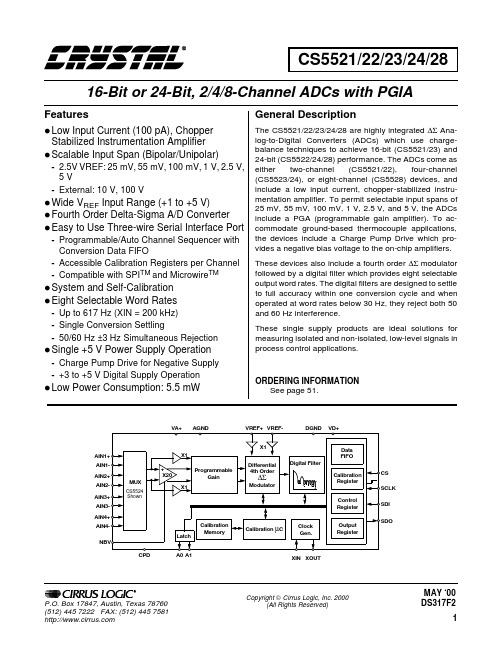
Copyright © Cirrus Logic, Inc. 2000CS5521/22/23/24/2816-Bit or 24-Bit, 2/4/8-Channel ADCs with PGIAFeaturesl Low Input Current (100pA), ChopperStabilized Instrumentation Amplifier l Scalable Input Span (Bipolar/Unipolar)-2.5V VREF: 25mV, 55mV, 100mV, 1V, 2.5V, 5V-External: 10V, 100 Vl Wide V REF Input Range (+1 to +5V)l Fourth Order Delta-Sigma A/D Converter l Easy to Use Three-wire Serial Interface Port-Programmable/Auto Channel Sequencer with Conversion Data FIFO-Accessible Calibration Registers per Channel -Compatible with SPI TM and Microwire TMl System and Self-Calibration l Eight Selectable Word Rates-Up to 617Hz (XIN =200kHz)-Single Conversion Settling-50/60Hz ±3Hz Simultaneous Rejectionl Single +5V Power Supply Operation-Charge Pump Drive for Negative Supply -+3 to +5V Digital Supply Operationl Low Power Consumption: 5.5mWGeneral DescriptionThe CS5521/22/23/24/28 are highly integrated ∆Σ Ana-log-to-Digital Converters (ADCs) which use charge-balance techniques to achieve 16-bit (CS5521/23) and 24-bit (CS5522/24/28) performance. The ADCs come as either two-channel (CS5521/22), four-channel (CS5523/24), or eight-channel (CS5528) devices, and include a low input current, chopper-stabilized instru-mentation amplifier. To permit selectable input spans of 25mV, 55mV, 100mV, 1V, 2.5V, and 5V, the ADCs include a PGA (programmable gain amplifier). To ac-commodate ground-based thermocouple applications,the devices include a Charge Pump Drive which pro-vides a negative bias voltage to the on-chip amplifiers.These devices also include a fourth order ∆Σ modulator followed by a digital filter which provides eight selectable output word rates . The digital filters are designed to settle to full accuracy within one conversion cycle and when operated at word rates below 30Hz, they reject both 50and 60Hz interference.These single supply products are ideal solutions for measuring isolated and non-isolated, low-level signals in process control applications.ORDERING INFORMATIONSee page 51.ProgrammableGainVA+AGND VREF+VREF-VD+DGND XIN XOUTSDOSDI NBVLatchDifferential Digital FilterCalibration Register Control RegisterOutput Register4th Order ∆ΣModulatorCalibration MemoryCalibration µCClock Gen.SCLK CS MUXAIN2++X20X1X1X1CS5524 ShownAIN2-AIN1+AIN1-AIN4+AIN4-AIN3+AIN3-A0A1CPDData FIFO MAY ‘00DS317F2TABLE OF CONTENTS1. CHARACTERISTICS AND SPECIFICATIONS (5)ANALOG CHARACTERISTICS (5)TYPICAL RMS NOISE, CS5521/23 (7)TYPICAL NOISE FREE RESOLUTION (BITS), CS5521/23 (7)TYPICAL RMS NOISE, CS5522/24/28 (8)TYPICAL NOISE FREE RESOLUTION (BITS), CS5522/24/28 (8)5 V DIGITAL CHARACTERISTICS (9)3 V DIGITAL CHARACTERISTICS (9)DYNAMIC CHARACTERISTICS (10)RECOMMENDED OPERATING CONDITIONS (10)ABSOLUTE MAXIMUM RATINGS (10)SWITCHING CHARACTERISTICS (11)2. GENERAL DESCRIPTION (13)2.1 Analog Input (13)2.1.1 Instrumentation Amplifier (14)2.1.2 Coarse/Fine Charge Buffers (14)2.1.3 Analog Input Span Considerations (15)2.1.4 Measuring Voltages Higher than 5 V (15)2.1.5 Voltage Reference (16)2.2 Overview of ADC Register Structure and Operating Modes (16)2.2.1 System Initialization (18)2.2.2 Serial Port Initialization Sequence (18)2.2.3 Command Register Quick Reference (19)2.2.4 Command Register Descriptions (20)2.2.5 Serial Port Interface (25)2.2.6 Reading/Writing the Offset, Gain, and Configuration Registers (26)2.2.7 Reading/Writing the Channel-Setup Registers (26)2.2.7.1 Latch Outputs (28)2.2.7.2 Channel Select Bits (28)2.2.7.3 Output Word Rate Selection (28)2.2.7.4 Gain Bits (28)2.2.7.5 Unipolar/Bipolar Bit (28)2.2.8 Configuration Register (28)2.2.8.1 Chop Frequency Select (28)2.2.8.2 Conversion/Calibration Control Bits (28)2.2.8.3 Power Consumption Control Bits (28)Contacting Cirrus Logic SupportFor a complete listing of Direct Sales, Distributor, and Sales Representative contacts, visit the Cirrus Logic web site at: /corporate/contacts/SPI™ is a trademark of Motorola Inc., Microwire™ is a trademark of National Semiconductor Corp.Preliminary product information describes products which are in production, but for which full characterization data is not yet available. Advance product information describes products which are in development and subject to development changes. Cirrus Logic, Inc. has made best efforts to ensure that the information contained in this document is accurate and reliable. However, the information is subject to change without notice and is provided “AS IS” without warranty of any kind (express or implied). No responsibility is assumed by Cirrus Logic, Inc. for the use of this information, nor for infringements of patents or other rights of third parties. This document is the property of Cirrus Logic, Inc. and implies no license under patents, copyrights, trademarks, or trade secrets. No part of this publication may be copied, reproduced, stored in a retrieval sys-tem, or transmitted, in any form or by any means (electronic, mechanical, photographic, or otherwise). Furthermore, no part of this publication may be used as a basis for manufacture or sale of any items without the prior written consent of Cirrus Logic, Inc. The names of products of Cirrus Logic, Inc. or other vendors and suppliers appearing in this document may be trademarks or service marks of their respective owners which may be registered in some jurisdictions. A list of Cirrus Logic, Inc. trademarks and service marks can be found at .2.2.8.4 Charge Pump Disable (29)2.2.8.5 Reset System Control Bits (29)2.2.8.6 Data Conversion Error Flags (29)2.3 Calibration (31)2.3.1 Self Calibration (31)2.3.2 System Calibration (32)2.3.3 Calibration Tips (34)2.3.4 Limitations in Calibration Range (34)2.4 Performing Conversions and Reading the Data Conversion FIFO (34)2.4.1 Conversion Protocol (35)2.4.1.1 Single, One-Setup Conversion (35)2.4.1.2 Repeated One-Setup Conversions without Wait (35)2.4.1.3 Repeated One-Setup Conversions with Wait (36)2.4.1.4 Single, Multiple-Setup Conversions (36)2.4.1.5 Repeated Multiple-Setup Conversions without Wait (37)2.4.1.6 Repeated Multiple-Setup Conversions with Wait (37)2.4.2 Calibration Protocol (38)2.4.3 Example of Using the CSRs to Perform Conversions and Calibrations (38)2.5 Conversion Output Coding (40)2.5.1 Conversion Data FIFO Descriptions (41)2.6 Digital Filter (42)2.7 Clock Generator (42)2.8 Power Supply Arrangements (43)2.8.1 Charge Pump Drive Circuits (45)2.9 Digital Gain Scaling (45)2.10 Getting Started (46)2.11 PCB Layout (47)3. PIN DESCRIPTIONS (48)3.1 Clock Generator (49)3.2 Control Pins and Serial Data I/O (49)3.3 Measurement and Reference Inputs (49)3.4 Power Supply Connections (50)4. SPECIFICATION DEFINITIONS (51)5. ORDERING GUIDE (51)6. PACKAGE DIMENSION DRAWINGS (52)LIST OF FIGURESFigure 1. Continuous Running SCLK Timing (Not to Scale) (12)Figure 2. SDI Write Timing (Not to Scale) (12)Figure 3. SDO Read Timing (Not to Scale) (12)Figure 4. Multiplexer Configurations (13)Figure 5. Input Models for AIN+ and AIN- pins, £(100 mV Input Ranges (14)Figure 6. Input Models for AIN+ and AIN- pins, >100 mV input ranges (14)Figure 7. Input Ranges Greater than 5 V (16)Figure 8. Input Model for VREF+ and VREF- Pins (16)Figure 9. CS5523/24 Register Diagram (17)Figure 10. Command and Data Word Timing (25)Figure 11. Self Calibration of Offset (Low Ranges) (32)Figure 12. Self Calibration of Offset (High Ranges) (32)Figure 13. Self Calibration of Gain (All Ranges) (32)Figure 14. System Calibration of Offset (Low Ranges) (32)Figure 15. System Calibration of Offset (High Ranges) (33)Figure 16. System Calibration of Gain (Low Ranges) (33)Figure 17. System Calibration of Gain (High Ranges) (33)Figure 18. Filter Response (Normalized to Output Word Rate = 1) (42)Figure 19. Typical Linearity Error for CS5521/23 (42)Figure 20. Typical Linearity Error for CS5522/24/28 (42)Figure 21. CS5522 Configured to use on-chip charge pump to supply NBV (43)Figure 22. CS5522 Configured for ground-referenced Unipolar Signals (44)Figure 23. CS5522 Configured for Single Supply Bridge Measurement (44)Figure 24. Charge Pump Drive Circuit for VD+ = 3 V (45)Figure 25. Alternate NBV Circuits (45)LIST OF TABLESTable 1. Relationship between Full Scale Input, Gain Factors, and Internal AnalogSignal Limitations (15)Table 2. Command Register Quick Reference (19)Table 3. Channel-Setup Registers (27)Table 4. Configuration Register (30)Table 5. Offset and Gain Registers (31)Table 6. Output Coding for 16-bit CS5521/23 and 24-bit CS5522/24/28 (40)1. CHARACTERISTICS AND SPECIFICATIONSANALOG CHARACTERISTICS (T A = 25° C; VA+, VD+ = 5 V ±5%; VREF+ = 2.5 V, VREF- = AGND,NBV = -2.1 V, XIN = 32.768 kHz, CFS1-CFS0 = ‘00’, OWR (Output Word Rate) = 15 Hz, Bipolar Mode, Input Range = ±100 mV; See Notes 1 and 2.)Notes: 1.Applies after system calibration at any temperature within -40° C ~ +85° C.2.Specifications guaranteed by design, characterization, and/or test.3.Specification applies to the device only and does not include any effects by external parasiticthermocouples. LSB N : N is 16 for the CS5521/23 and N is 24 for the CS5522/24/284.Drift over specified temperature range after calibration at power-up at 25° C.5.Measured with Charge Pump Drive off.6.All outputs unloaded. All input CMOS levels and the CS5521/23 do not have a low power mode.ParameterCS5521/23CS5522/24/28Unit Min Typ Max Min Typ Max Accuracy Resolution --16--24Bits Linearity Error -±0.0015±0.003-±0.0007±0.0015%FS Bipolar Offset (Note 3)-±1±2-±16±32LSB N Unipolar Offset (Note 3)-±2±4-±32±64LSB N Offset Drift (Notes 3 and 4)-20--20-nV/°C Bipolar Gain Error -±8±31-±8±31ppm Unipolar Gain Error -±16±62-±16±62ppm Gain Drift (Note 4)-13-13ppm/°CPower SuppliesPower Supply Currents (Normal Mode)I A+(Note 5)I D+I NBV- - - 0.990260 1.2135375 - - - 1.590525 1.9135700mA µA µA Power Consumption (Note 6)Normal Mode Low Power Mode Standby Sleep-N/A -- 5.5N/A 1.25007.5N/A ------95.51.2500127.5--mW mW mW µW Power Supply RejectionPositive Supplies dc NBV--120110----120110--dB dBANALOG CHARACTERISTICS (Continued)Notes:7.For the CS5528, the 25mV, 55mV and 100mV ranges cannot be used unless NBV is powered at -1.8to -2.5V8.See the section of the data sheet which discusses input models. Chop clock is 256Hz (XIN/128) forPGIA (programmable gain instrumentation amplifier). XIN = 32.768kHz.9.The maximum full scale signal can be limited by saturation of circuitry within the internal signal path.ParameterMin TypMaxUnitAnalog InputCommon Mode + Signal on AIN+ or AIN-Bipolar/Unipolar ModeNBV = -1.8 to -2.5 V Range = 25 mV, 55 mV, or 100 mVRange = 1 V, 2.5 V, or 5 VNBV = AGND Range = 25 mV, 55 mV, or 100 mV (Note 7)Range = 1 V, 2.5 V, or 5 V-0.150NBV 1.850.0----0.950VA+2.65VA+V V V V CVF Current on AIN+ or AIN-(Note 8)Range = 25 mV, 55 mV, or 100 mV Range = 1 V, 2.5 V, or 5 V--10010300-pA nA Input Current Drift (Note 8)Range = 25 mV, 55 mV, or 100 mV-1-pA/°C Input Leakage for Multiplexer when Off -10-pA Common Mode Rejection dc50, 60 Hz--120120--dB dB Input Capacitance-10-pF Voltage Reference Input Range (VREF+) - (VREF-)12.5VA+V VREF+(VREF-)+1-VA+V VREF-NBV -(VREF+)-1V CVF Current (Note 8)- 5.0-nA Common Mode Rejection dc50, 60 Hz--110130--dB dB Input Capacitance-16-pFSystem Calibration SpecificationsFull Scale Calibration Range (VREF = 2.5V)Bipolar/Unipolar Mode25 mV 55 mV 100 mV 1 V 2.5 V 5 V1025400.401.02.0------32.571.51051.303.25VA+mV mV mV V V V Offset Calibration Range Bipolar/Unipolar Mode25 mV 55 mV 100 mV (Note 9)1 V 2.5 V 5 V------------±12.5±27.5±50±0.5±1.25±2.50mV mV mV V V VTYPICAL RMS NOISE, CS5521/23 (Notes 10 and 11)Notes:10.Wideband noise aliased into the baseband. Referred to the input. Typical values shown for 25° C.11.To estimate Peak-to-Peak Noise, multiply RMS noise by 6.6 for all ranges and output rates.12.For input ranges <100mV and output rates ≥60Hz, 16.384kHz chopping frequency is used.TYPICAL NOISE FREE RESOLUTION (BITS), CS5521/23 (Note 13)Notes:13.For bipolar mode, the number of bits of Noise Free Resolution is LOG((2XInput Range)/(6.6xRMSNoise))/LOG(2) rounded to the nearest bit. For unipolar mode, the number of bits of Noise Free Resolution is LOG((Input Range)/(6.6xRMS Noise))/LOG(2) rounded to the nearest bit. Also, the CS5521/23’s output conversions are 16 bits. Noise free Resolution numbers are based uponVREF =2.5V and XIN =32.768kHz. The values will be affected directly by changes in VREF, but the effects due to changes in the XIN frequency will be minor.Output Rate (Hz)-3 dB FilterFrequency Input Range, (Bipolar/Unipolar Mode)25 mV55 mV 100 mV 1 V 2.5 V 5 V1.88 1.6490 nV 148 nV 220 nV 1.8 µV 3.9 µV 7.8 µV 3.76 3.27122 nV 182 nV 310 nV2.6 µV 5.7 µV 11.3 µV 7.51 6.55180 nV 267 nV 435 nV3.7 µV 8.5 µV 18.1 µV 15.012.7280 nV 440 nV 810 nV 5.7 µV 14 µV 28 µV 30.025.4580 nV 1.1 µV 2.1 µV 18.2 µV 48 µV 96 µV 61.6 (Note 12)50.4 2.6 µV4.9 µV 8.5 µV 92 µV 238 µV 390 µV 84.5 (Note 12)70.711 µV 27 µV 43 µV 458 µV 1.1 mV 2.4 mV 101.1 (Note 12)84.641 µV72 µV 130 µV 1.2 mV 3.4 mV6.7 mVOutput Rate (Hz)-3 dB FilterFrequency Input Range, (Bipolar Mode)25 mV55 mV 100 mV 1 V 2.5 V5 V 1.88 1.641616161616163.76 3.271616161616167.51 6.5515161616161615.012.715151516161630.025.414141414141461.6 (Note 12)50.412121212121284.5 (Note 12)70.7999999101.1 (Note 12)84.6888888TYPICAL RMS NOISE, CS5522/24/28 (Notes 14 and 15)Notes:14.Wideband noise aliased into the baseband. Referred to the input. Typical values shown for 25° C.15.To estimate Peak-to-Peak Noise, multiply RMS noise by 6.6 for all ranges and output rates.16.For input ranges <100mV and output rates ≥60Hz, 16.384kHz chopping frequency is used.TYPICAL NOISE FREE RESOLUTION (BITS), CS5522/24/28 (Note 17)Notes:17.For bipolar mode, the number of bits of Noise Free Resolution is LOG((2XInput Range)/(6.6xRMSNoise))/LOG(2) rounded to the nearest bit. For unipolar mode, the number of bits of Noise Free Resolution is LOG((Input Range)/(6.6xRMS Noise))/LOG(2) rounded to the nearest bit. Also, the CS5522/24/28’s output conversions are 24 bits. Noise free Resolution numbers are based uponVREF =2.5V and XIN =32.768kHz. The values will be affected directly by changes in VREF, but the effects due to changes in the XIN frequency will be minor.Output Rate (Hz)-3 dB FilterFrequency Input Range, (Bipolar/Unipolar Mode)25 mV55 mV 100 mV 1 V 2.5 V 5 V1.88 1.6490 nV 95 nV 140 nV 1.5 µV 3 µV 6 µV 3.76 3.27110 nV 130 nV 190 nV 2 µV 4 µV 8 µV 7.51 6.55170 nV 200 nV 275 nV2.5 µV 6 µV 11.5 µV 15.012.7250 nV 330 nV 580 nV 4.5 µV 10 µV 20 µV 30.025.4500 nV 1 µV 1.5 µV 16 µV 45 µV 85 µV 61.6 (Note 16)50.4 2 µV 4 µV 8 µV 72 µV 195 µV 350 µV 84.5 (Note 16)70.710 µV 20 µV 35 µV 340 µV 900 µV 2 mV 101.1 (Note 16)84.630 µV60 µV 105 µV 1.1 mV 3 mV5.3 mVOutput Rate (Hz)-3 dB FilterFrequency Input Range, (Bipolar Mode)25 mV55 mV 100 mV 1 V 2.5 V5 V 1.88 1.641617181818183.76 3.271617171718187.51 6.5515161717171715.012.715161616161630.025.414141414141461.6 (Note 16)50.412121212121284.5 (Note 16)70.7101010101010101.1 (Note 16)84.68888885 V DIGITAL CHARACTERISTICS (T A = 25° C; VA+, VD+ = 5 V ±5%; GND = 0;See Notes 2 and 18.))Notes:18.All measurements performed under static conditions.19.I out = -100µA unless stated otherwise. (V OH = 2.4 V @ I out = -40µA.)3 V DIGITAL CHARACTERISTICS (T A = 25° C; VA+ = 5 V ±5%; VD+ = 3.0 V ±10%; GND = 0;See Notes 2 and 18.)ParameterSymbol Min Typ Max Unit High-Level Input VoltageAll Pins Except XIN and SCLKXIN SCLK V IH0.6 VD+(VD+)-0.5(VD+) - 0.45------V V V Low-Level Input VoltageAll Pins Except XIN and SCLKXIN SCLKV IL------0.81.50.6V V V High-Level Output VoltageAll Pins Except CPD and SDO (Note 19)CPD, I out = -4.0 mA SDO, I out = -5.0 mA V OH(VA+) - 1.0(VD+) - 1.0(VD+) - 1.0------V V V Low-Level Output VoltageAll Pins Except CPD and SDO, I out = 1.6 mACPD, I out = 2 mA SDO, I out = 5.0 mA V OL------0.40.40.4V V V Input Leakage Current I in -±1±10µA 3-State Leakage Current I OZ --±10µA Digital Output Pin CapacitanceC out-9-pFParameterSymbol Min Typ Max Unit High-Level Input VoltageAll Pins Except XIN and SCLKXIN SCLK V IH0.6 VD+(VD+)-0.5(VD+) - 0.45------V V V Low-Level Input VoltageAll Pins Except XIN and SCLKXIN SCLKV IL------0.16 VD+0.30.6V V V High-Level Output VoltageAll Pins Except CPD and SDO, I out = -400 µACPD, I out = -4.0 mA SDO, I out = -5.0 mA V OH(VA+) - 0.3(VD+) - 1.0(VD+) - 1.0------V V V Low-Level Output VoltageAll Pins Except CPD and SDO, I out = 400 µACPD, I out = 2 mA SDO, I out = 5.0 mA V OL------0.30.40.4V V V Input Leakage Current I in -±1±10µA 3-State Leakage Current I OZ --±10µA Digital Output Pin CapacitanceC out-9-pFDYNAMIC CHARACTERISTICSRECOMMENDED OPERATING CONDITIONS (AGND, DGND = 0 V; See Note 20.)Notes:20.All voltages with respect to ground.ABSOLUTE MAXIMUM RATINGS (AGND, DGND = 0 V; See Note 20.)Notes:21.No pin should go more negative than NBV - 0.3V.22.Applies to all pins including continuous overvoltage conditions at the analog input (AIN) pins.23.Transient current of up to 100mA will not cause SCR latch-up. Maximum input current for a powersupply pin is ±50mA.24.Total power dissipation, including all input currents and output currents.WARNING:Operation at or beyond these limits may result in permanent damage to the device.Normal operation is not guaranteed at these extremes.ParameterSymbol Ratio Unit Modulator Sampling Frequencyf s XIN/4Hz Filter Settling Time to 1/2 LSB (Full Scale Step)t s1/f outsParameterSymbol Min Typ Max Unit DC Power Supplies Positive Digital Positive Analog VD+VA+ 2.74.75 5.05.0 5.255.25V V Analog Reference Voltage (VREF+) - (VREF-)VRef diff 1.0 2.5VA+V Negative Bias VoltageNBV-1.8-2.1-2.5VParameterSymbol Min Typ Max Unit DC Power Supplies(Note 21)Positive Digital Positive Analog VD+VA+-0.3-0.3--+6.0+6.0V V Negative Bias VoltageNegative Potential NBV +0.3-2.1-3.0V Input Current, Any Pin Except Supplies (Note 22 and 23)I IN --±10mA Output Current I OUT --±25mA Power Dissipation (Note 24)PDN --500mW Analog Input Voltage VREF pins AIN PinsV INR V INA NBV -0.3NBV -0.3--(VA+) + 0.3(VA+) + 0.3V V Digital Input VoltageV IND -0.3-(VD+) + 0.3V Ambient Operating Temperature T A -40-85°C Storage TemperatureT stg-65-150°CSWITCHING CHARACTERISTICS (T A = 25° C; VA+ = 5 V ±5%; VD+ = 3.0 V ±10% or 5 V ±5%;Levels: Logic 0 = 0 V, Logic 1 = VD+; C L = 50 pF.))Notes:25.Device parameters are specified with a 32.768kHz clock; however, clocks up to 200kHz(CS5522/24/28) or 130kHz (CS5521/23) can be used for increased throughput.26.Specified using 10% and 90% points on waveform of interest. Output loaded with 50pF.27.Oscillator start-up time varies with crystal parameters. This specification does not apply when using anexternal clock source.28.Applicable when SCLK is continuously running.Specifications are subject to change without notice.ParameterSymbol Min Typ MaxUnitMaster Clock Frequency (Note 25)External Clock or Internal Oscillator (CS5522/24/28)(CS5521/23)XIN303032.76832.768200130kHz kHz Master Clock Duty Cycle 40-60%Rise Times(Note 26)Any Digital Input Except SCLKSCLKAny Digital Output t rise-----50 1.0100-µs µs ns Fall Times(Note 26)Any Digital Input Except SCLKSCLKAny Digital Output t fall-----50 1.0100-µs µs ns Start-upOscillator Start-up Time XTAL = 32.768 kHz(Note 27)t ost -500-ms Power-on Reset Period t por-2006-XIN cycles Serial Port Timing Serial Clock FrequencySCLK 0-2MHz SCLK Falling to CS Falling for continuous running SCLK(Note 28)t 0100--ns Serial ClockPulse Width High Pulse Width Lowt 1t 2250250----ns ns SDI Write TimingCS Enable to Valid Latch Clock t 350--ns Data Set-up Time prior to SCLK rising t 450--ns Data Hold Time After SCLK Rising t 5100--ns SCLK Falling Prior to CS Disablet 6100--ns SDO Read TimingCS to Data Validt 7--150ns SCLK Falling to New Data Bit t 8--150ns CS Rising to SDO Hi-Zt 9--150nsFigure 1. Continuous Running SCLK Timing (Not to Scale)Figure 2. SDI Write Timing (Not to Scale)Figure 3. SDO Read Timing (Not to Scale)2. GENERAL DESCRIPTIONThe CS5521/22/23/24/28 are highly integrated ∆ΣAnalog-to-Digital Converters (ADCs) which use charge-balance techniques to achieve 16-bit (CS5521/23) and 24-bit (CS5522/24/28) perfor-mance. The ADCs come as either two-channel (CS5521/22), four-channel (CS5523/24), or eight-channel (CS5528) devices, and include a low input current, chopper-stabilized instrumentation ampli-fier. To permit selectable input spans of 25mV, 55mV, 100mV, 1V, 2.5V, and 5V, the ADCs in-clude a PGA (programmable gain amplifier). To accommodate ground-based thermocouple applica-tions, the devices include a CPD (Charge Pump Drive) which provides a negative bias voltage to the on-chip amplifiers.These devices also include a fourth order DS mod-ulator followed by a digital filter which provides eight selectable output word rates of 1.88Hz, 3.76Hz, 7.51Hz, 15Hz, 30Hz, 61.6Hz, 84.5Hz, and 101.1Hz (XIN=32.768kHz). The devices are capable of producing output update rates up to 617Hz when a 200kHz clock is used (CS5522/24/28) or up to 401Hz using a 130kHz clock (CS5521/23). Further note that the digital fil-ters are designed to settle to full accuracy within one conversion cycle and simultaneously reject both 50Hz and 60Hz interference when operated at word rates below 30Hz (assuming a XIN clock frequency of 32.768kHz).To ease communication between the ADCs and a micro-controller, the converters include an easy to use three-wire serial interface which is SPI™ and Microwire™ compatible.2.1 Analog InputFigure4 illustrates a block diagram of the analog in-put signal path inside the CS5521/22/23/24/28. The front end consists of a multiplexer (break before make configuration), a chopper-stabilized instru-mentation amplifier with fixed gain of 20X, coarse/fine charge buffers, and a programmable gain section. For the 25mV, 55mV, and 100mV input ranges, the input signals are amplified by the 20X in-strumentation amplifier. For the 1V, 2.5V, and 5V input ranges, the instrumentation amplifier is by-passed and the input signals are connected to the Programmable Gain block via coarse/fine charge buffers.Figure 4. Multiplexer Configurations2.1.1 Instrumentation AmplifierThe instrumentation amplifier is chopper stabilized and is activated any time conversions are performed with the low level input ranges, ≤100mV. The am-plifier is powered from VA+ and from the NBV (Negative Bias Voltage) pin allowing the CS5521/22/23/24/28 to be operated in either of two analog input configurations. The NBV pin can be bi-ased to a negative voltage between -1.8V and -2.5V, or tied to AGND (for the CS5528, NBV has to be between -1.8V and -2.5V for the ranges below 100mV when the amplifier is engaged). The com-mon-mode plus signal range of the instrumentation amplifier is 1.85V to 2.65V with NBV grounded. The common-mode plus signal range of the instru-mentation amplifier is -0.150V to 0.950V with NBV between -1.8V to -2.5V. Whether NBV is tied between -1.8V and -2.5V or tied to AGND, the (Common Mode + Signal) input on AIN+ and AIN- must stay between NBV and VA+.Figure5illustrates an analog input model for the ADCs when the instrumentation amplifier is en-gaged. The CVF (sampling) input current for each of the analog input pins depends on the CFS1 and CFS0 (Chop Frequency Select) bits in the configu-ration register (see Configuration Register for de-tails). Note that the CVF current is lowest with the CFS bits in their default states (cleared to logic 0s). Further note that the CVF current into the instru-mentation amplifier is less than 300 pA over -40°C to +85°C. Note that Figure5 is for input current modeling only. For physical input capacitance see ‘Input Capacitance’ specification under ANALOG CHARACTERISTICS. Also refer to Applications Note AN30 “Switched-Capacitor A/D Converter Input Structures” for more details on input models and input sampling currents.Note: Residual noise appears in the converter’s baseband for output word rates greater than 61.6Hz if the CFS bits are logic 0 (chop clock=256Hz). For word rates of 30Hz and lower, 256Hz chopping is recommended, and for 61.6Hz, 84.5Hz and 101.1Hz filters, 4096Hz chopping is recommended.2.1.2 Coarse/Fine Charge BuffersThe unity gain buffers are activated any time conver-sions are performed with the high level inputs rang-es, 1V, 2.5V, and 5V. The unity gain buffers are designed to accommodate rail to rail input signals. The common-mode plus signal range for the unity gain buffer amplifier is NBV to VA+.Typical CVF (sampling) current for the unity gain buffer amplifiers is about 10nA (XIN=32.768kHz, see Figure6).Figure 5. Input Models for AIN+ and AIN- pins, ≤(100 mV Input Ranges Figure 6. Input Models for AIN+ and AIN- pins,>100 mV input ranges2.1.3 Analog Input Span ConsiderationsThe CS5521/22/23/24/28 is designed to measure full scale ranges of 25mV, 55mV, 100mV, 1V,2.5V and 5V. Other full scale values can be ac-commodated by performing a system calibration within the limits specified. See the Calibration sec-tion for more details. Another way to change the full scale range is to increase or to decrease the voltage reference to a voltage other than 2.5 . See the Voltage Reference section for more details. Three factors set the operating limits for the input span. They include: instrumentation amplifier satu-ration, modulator 1’s density, and a lower reference voltage. When the 25mV, 55mV or 100mV range is selected, the input signal (including the common mode voltage and the amplifier offset voltage)must not cause the 20X amplifier to saturate in ei-ther its input stage or output stage. To prevent sat-uration the absolute voltages on AIN+ and AIN-must stay within the limits specified (refer to the Analog Input section). Additionally, the differen-tial output voltage of the amplifier must not exceed 2.8V. The equationABS(VIN + VOS) x 20 = 2.8Vdefines the differential output limit, whereVIN = (AIN+) - (AIN-)is the differential input voltage and VOS is the ab-solute maximum offset voltage for the instrumenta-tion amplifier (VOS will not exceed 40mV). If the differential output voltage from the amplifier ex-ceeds 2.8V, the amplifier may saturate, which will cause a measurement error.The input voltage into the modulator must not cause the modulator to exceed a low of 20 percent or a high of 80 percent 1's density. The nominal full scale input span of the modulator (from 30 percent to 70 percent 1’s density) is determined by the VREF voltage divided by the Gain Factor. See Table 1 to determine if the CS5521/22/23/24/28are being used properly. For example, in the 55mV range, to determine the nominal input volt-age to the modulator, divide VREF (2.5V) by the Gain Factor (2.2727).When a smaller voltage reference is used, the re-sulting code widths are smaller causing the con-verter output codes to exhibit more changing codes for a fixed amount of noise. Table 1 is based upon a VREF =2.5V. For other values of VREF, the values in Table 1 must be scaled accordingly.2.1.4 Measuring Voltages Higher than 5 VSome systems require the measurement of voltages greater than 5V. The input current of the instru- Note:1.The converter’s actual input range, the delta-sigma’s nominal full scale input, and the delta-sigma’smaximum full scale input all scale directly with the value of the voltage reference. The values in the table assume a 2.5 V VREF voltage.2.The 2.8V limit at the output of the 20X amplifier is the differential output voltage.Input Range (1)Max. Differential Output20X AmplifierVREF Gain Factor∆-Σ Nominal (1)Differential Input∆-Σ(1)Max. Input ±25 mV 2.8 V (2) 2.5V 5±0.5 V ±0.75 V ±55 mV 2.8 V (2) 2.5V 2.272727...±1.1 V ±1.65 V ±100 mV 2.8 V (2)2.5V 1.25±2.0 V ±3.0 V ±1.0 V - 2.5V 2.5±1.0 V ±1.5 V ±2.5 V - 2.5V 1.0±2.5 V ±5.0 V ±5.0 V- 2.5V0.5±5.0 V0V, VA+Table 1. Relationship between Full Scale Input, Gain Factors, and Internal AnalogSignal Limitations。

自适应Shearlet域约束的全变差图像去噪朱华生;邓承志【期刊名称】《计算机工程》【年(卷),期】2013(039)001【摘要】采用传统非线性扩散图像去嗓方法得到的图像边缘模糊,为此,提出一种有限自适应Shearlet域约束的极小化变分图像去噪算法.通过自适应阈值收缩Shearlet系数,保留图像纹理与边缘空间,利用全变差极小化平滑空间,建立全变差正则化的能量泛函去噪模型.实验结果表明,该算法能在减少图像噪声的同时,保留图像边缘信息,对含有丰富纹理结构的图像,去噪性能更佳.%In this paper, an adaptive Shearlet domain regularized minimization total variation image denoising algorithm is proposed, which can overcome the problem of the traditional nonlinear diffusion image denoising methods. The texture and edge domain is adaptively shrinkaged in Shearlet domain. And then, a total variation regularized energy functional model with restrictions on the finite adaptive shearlet domain is used to deal with smooth domain. Experimental results show that this algorithm can reduce the noise and preserve the edge information, especially to the images containing abundant texture.【总页数】4页(P221-224)【作者】朱华生;邓承志【作者单位】南昌工程学院信息工程学院,南昌330099;南昌工程学院信息工程学院,南昌330099【正文语种】中文【中图分类】TN919.73【相关文献】1.Shearlet变换域自适应图像去噪算法 [J], 朱华生;徐晨光2.基于自适应shearlet域约束下的图像去噪研究 [J], 王丰斌;杨坷巍3.非下采样Shearlet域多变量模型的图像去噪 [J], 刘巧红;林敏;李广超4.基于自适应shearlet域约束下的图像去噪研究 [J], 王丰斌;杨坷巍5.一种改进全变差正则化的Shearlet自适应带钢图像去噪算法 [J], 韩英莉因版权原因,仅展示原文概要,查看原文内容请购买。

AAMI TIR29:2002技术信息报告辐照灭菌过程控制指南AAMI 美国医疗器械促进协会(Association for the Advancement of MEDICALInstrumentation)AAMI 技术信息报告AAMI TIR29:2002辐照灭菌过程控制指南Approved 16 July 2002 by美国医疗器械促进协会摘要: 本技术信息报告增加了ANSI/AAMI/ISO 11137所界定的光子,电子束灭菌的剂量场的建立和规范,过程确认,和常规控制等辐射灭菌。
尽管轫致辐射的要求相似,但在这项工作开始的时候缺乏关于轫致辐射装置的设计和运行的经验。
所以轫致辐射不包括在此指南之内。
关键词: 辐射剂量场, 过程确认, 日常加工,剂量确认美国医疗器械促进协会技术信息报告信息技术报告是美国医疗器械促进协会标准局的刊物,它是为特殊的医疗技术提供。
提交到信息技术报告的材料需要更多专家的意见,发表的信息也得是用的,因为很多行业都急切需要它。
信息技术报告与标准和操作规程建议,读者应该理解这些文件的不同之处。
标准和工业标准由正式的委员会通过收集所有正确的意见和观点,此过程由美国医疗器械促进协会标准局和美国国际标准机构完成。
信息技术报告作为一个标准审核的过程不是一样。
但是,信息技术报告由技术委员会和美国医疗器械促进协会标准出版社发布。
另外一个不同的地方,尽管标准和信息技术报告都需要定期审查,一个标准必须经过重申,修改,或撤回,通常每五年或十年需要正式的被认可。
对于信息技术报告来说,美国医疗器械促进协会和技术委员会达成一致,规定自出版日期五年后(作为一个周期)进行审查报告是否有用,检查信息是否切题和具有实用性,如果信息没有实用性了,此信息技术报告就被删掉。
信息技术报告肯发展,因为它比标准和操作规程建议能更好响应基础安全和性能问题。
或者说因为达成共识是非常困难甚至不可能。
信息技术报告与标准不同,它允许在技术问题上由不同的观点。
MPU-6881 Product Specification Revision 1.0TABLE OF CONTENTSTABLE OF FIGURES (4)TABLE OF TABLES (5)1DOCUMENT INFORMATION (6)1.1R EVISION H ISTORY (6)1.2P URPOSE AND S COPE (7)1.3P RODUCT O VERVIEW (7)1.4A PPLICATIONS (7)2FEATURES (8)2.1G YROSCOPE F EATURES (8)2.2A CCELEROMETER F EATURES (8)2.3A DDITIONAL F EATURES (8)3ELECTRICAL CHARACTERISTICS (9)3.1G YROSCOPE S PECIFICATIONS (9)3.2A CCELEROMETER S PECIFICATIONS (10)3.3E LECTRICAL S PECIFICATIONS (11)3.4I2C T IMING C HARACTERIZATION (15)3.5SPI T IMING C HARACTERIZATION (16)3.6A BSOLUTE M AXIMUM R ATINGS (18)4APPLICATIONS INFORMATION (19)4.1P IN O UT D IAGRAM AND S IGNAL D ESCRIPTION (19)4.2T YPICAL O PERATING C IRCUIT (20)4.3B ILL OF M ATERIALS FOR E XTERNAL C OMPONENTS (20)4.4B LOCK D IAGRAM (21)4.5O VERVIEW (21)4.6T HREE-A XIS MEMS G YROSCOPE WITH 16-BIT ADC S AND S IGNAL C ONDITIONING (22)4.7T HREE-A XIS MEMS A CCELEROMETER WITH 16-BIT ADC S AND S IGNAL C ONDITIONING (22)4.8I2C AND SPI S ERIAL C OMMUNICATIONS I NTERFACES (22)4.9S ELF-T EST (24)4.10C LOCKING (25)4.11S ENSOR D ATA R EGISTERS (25)4.12FIFO (25)4.13I NTERRUPTS (25)4.14D IGITAL-O UTPUT T EMPERATURE S ENSOR (25)4.15B IAS AND LDO S (26)4.16C HARGE P UMP (26)4.17S TANDARD P OWER M ODES (26)5PROGRAMMABLE INTERRUPTS (27)6DIGITAL INTERFACE (28)6.1I2C AND SPI S ERIAL I NTERFACES (28)6.2I2C I NTERFACE (28)6.3I2C C OMMUNICATIONS P ROTOCOL (28)6.4I2C T ERMS (31)6.5SPI I NTERFACE (32)7SERIAL INTERFACE CONSIDERATIONS (32)7.1MPU-6881S UPPORTED I NTERFACES (33)8ASSEMBLY (34)8.1O RIENTATION OF A XES (34)8.2P ACKAGE D IMENSIONS (35)9PART NUMBER PACKAGE MARKING (36)10RELIABILITY (37)10.1Q UALIFICATION T EST P OLICY (37)10.2Q UALIFICATION T EST P LAN (37)11REFERENCE (38)Table of FiguresFigure 1 I2C Bus Timing Diagram (15)Figure 2 SPI Bus Timing Diagram (16)Figure 3 Pin out Diagram for MPU-6881 3.0x3.0x0.9mm QFN (19)Figure 4 MPU-6881 QFN Application Schematic. (a) I2C operation, (b) SPI operation. (20)Figure 5 MPU-6881 Block Diagram (21)Figure 6 MPU-6881 Solution Using I2C Interface (23)Figure 7 MPU-6881 Solution Using SPI Interface (24)Figure 8 START and STOP Conditions (29)Figure 9 Acknowledge on the I2C Bus (29)Figure 10 Complete I2C Data Transfer (30)Figure 11 Typical SPI Master / Slave Configuration (32)Figure 12 I/O Levels and Connections (33)Figure 13 Orientation of Axes Sensitivity and Polarity of Rotation (34)Table of TablesTable 1 Gyroscope Specifications (9)Table 2 Accelerometer Specifications (10)Table 3 D.C. Electrical Characteristics (11)Table 4 A.C. Electrical Characteristics (13)Table 5 Other Electrical Specifications (14)Table 6 I2C Timing Characteristics (15)Table 7 SPI Timing Characteristics (16)Table 8 fCLK = 20MHz (17)Table 9 Absolute Maximum Ratings (18)Table 10 Signal Descriptions (19)Table 11 Bill of Materials (20)Table 12 Standard Power Modes for MPU-6881 (26)Table 13 Table of Interrupt Sources (27)Table 14 Serial Interface (28)Table 15 I2C Terms (31)1 Document Information1.2 Purpose and ScopeThis document is a preliminary product specification, providing a description, specifications, and design related information on the MPU-6881™ MotionTracking device. The device is housed in a small 3x3x0.9mm 24-pin QFN package.Specifications are subject to change without notice. Final specifications will be updated based upon characterization of production silicon. For references to register map and descriptions of individual registers, please refer to the MPU-6881 Register Map and Register Descriptions document.1.3 Product OverviewThe MPU-6881 is a 6-axis MotionTracking device that combines a 3-axis gyroscope, and a 3-axis accelerometer in a small 3x3x0.9mm (24-pin QFN) package. It also features a 4096-byte FIFO that can lower the traffic on the serial bus interface, and reduce power consumption by allowing the system processor to burst read sensor data and then go into a low-power mode. With its dedicated I2C sensor bus, the MPU-6881 directly accepts inputs from external I2C devices. MPU-6881, with its 6-axis integration, enables manufacturers to eliminate the costly and complex selection, qualification, and system level integration of discrete devices, guaranteeing optimal motion performance for consumers. MPU-6881 is also designed to interface with multiple non-inertial digital sensors, such as pressure sensors, on its auxiliary I2C port.The gyroscope has a programmable full-scale range of ±250, ±500, ±1000, and ±2000 degrees/sec. The accelerometer has a user-programmable accelerometer full-scale range of ±2g, ±4g, ±8g, and ±16g. Factory-calibrated initial sensitivity of both sensors reduces production-line calibration requirements.Other industry-leading features include on-chip 16-bit ADCs, programmable digital filters, a precision clock with 1% drift from -40°C to 85°C, an embedded temperature sensor, and programmable interrupts. The device features I2C and SPI serial interfaces, a VDD operating range of 1.71 to 3.45V, and a separate digital IO supply, VDDIO from 1.71V to 3.45V.Communication with all registers of the device is performed using either I2C at 400kHz or SPI at 1MHz. For applications requiring faster communications, the sensor and interrupt registers may be read using SPI at 20MHz.By leveraging its patented and volume-proven CMOS-MEMS Fabrication platform, which integrates MEMS wafers with companion CMOS electronics through wafer-level bonding, InvenSense has driven the package size down to a footprint and thickness of 3x3x0.9mm (24-pin QFN), to provide a very small yet high performance low cost package. The device provides high robustness by supporting 10,000g shock reliability.1.4 Applications∙TouchAnywhere™ technology (for “no touch” UI Application Control/Navigation)∙MotionCommand™ technology (for Gesture S hort-cuts)∙Motion-enabled game and application framework∙Location based services, points of interest, and dead reckoning∙Handset and portable gaming∙Motion-based game controllers∙3D remote controls for Internet connected DTVs and set top boxes, 3D mice∙Wearable sensors for health, fitness and sports2 Features2.1 Gyroscope FeaturesThe triple-axis MEMS gyroscope in the MPU-6881 includes a wide range of features:∙Digital-output X-, Y-, and Z-axis angular rate sensors (gyroscopes) with a user-programmable full-scale range of ±250, ±500, ±1000, and ±2000°/sec and integrated 16-bit ADCs ∙Digitally-programmable low-pass filter∙Gyroscope operating current: 3.2mA∙Factory calibrated sensitivity scale factor∙Self-test2.2 Accelerometer FeaturesThe triple-axis MEMS accelerometer in MPU-6881 includes a wide range of features:∙Digital-output X-, Y-, and Z-axis accelerometer with a programmable full scale range of ±2g, ±4g, ±8g and ±16g and integrated 16-bit ADCs∙Accelerometer normal operating current: 450µA∙Low power accelerometer mode current: 7.27µA at 0.98Hz, 18.65µA at 31.25Hz∙User-programmable interrupts∙Wake-on-motion interrupt for low power operation of applications processor∙Self-test2.3 Additional FeaturesThe MPU-6881 includes the following additional features:∙Auxiliary master I2C bus for reading data from external sensors (e.g. magnetometer)∙ 3.4mA operating current when all 6 motion sensing axes are active∙VDD supply voltage range of 1.8 – 3.3V ± 5%∙VDDIO reference voltage of 1.8 – 3.3V ± 5% for auxiliary I2C devices∙Smallest and thinnest QFN package for portable devices: 3x3x0.9mm (24-pin QFN)∙Minimal cross-axis sensitivity between the accelerometer and gyroscope axes∙4096 byte FIFO buffer enables the applications processor to read the data in bursts∙Digital-output temperature sensor∙User-programmable digital filters for gyroscope, accelerometer, and temp sensor∙10,000 g shock tolerant∙400kHz Fast Mode I2C for communicating with all registers∙1MHz SPI serial interface for communicating with all registers∙20MHz SPI serial interface for reading sensor and interrupt registers∙MEMS structure hermetically sealed and bonded at wafer level∙RoHS and Green compliant3 Electrical Characteristics3.1 Gyroscope SpecificationsTypical Operating Circuit of section 4.2, VDD = 1.8V, VDDIO = 1.8V, T A=25°C, unless otherwise noted.Please refer to the following document for information on Self-Test: MPU-6500 Accelerometer and Gyroscope Self-Test Implementation; AN-MPU-6500A-02.Table 1 Gyroscope SpecificationsNotes:1. Derived from validation or characterization of parts, not guaranteed in production.3.2 Accelerometer SpecificationsTypical Operating Circuit of section 4.2, VDD = 1.8V, VDDIO = 1.8V, T A=25°C, unless otherwise noted.Please refer to the following document for information on Self-Test: MPU-6500 Accelerometer and Gyroscope Self-Test Implementation; AN-MPU-6500A-02.Table 2 Accelerometer SpecificationsNotes:1. Derived from validation or characterization of parts, not guaranteed in production.3.3 Electrical Specifications3.3.1 D.C. Electrical CharacteristicsTypical Operating Circuit of section 4.2, VDD = 1.8V, VDDIO = 1.8V, T A=25°C, unless otherwise noted.Table 3 D.C. Electrical CharacteristicsNotes:1. Derived from validation or characterization of parts, not guaranteed in production.2. Accelerometer Low Power Mode supports the following output data rates (ODRs): 0.24, 0.49, 0.98,1.95, 3.91, 7.81, 15.63, 31.25, 62.50, 125, 250, 500Hz. Supply current for any update rate can becalculated as:a. Supply Current in µA = 6.9 + Update Rate * 0.3763.3.2 A.C. Electrical CharacteristicsTypical Operating Circuit of section 4.2, VDD = 1.8V, VDDIO = 1.8V, T A=25°C, unless otherwise noted.Table 4 A.C. Electrical CharacteristicsNotes:1. Derived from validation or characterization of parts, not guaranteed in production.3.3.3 Other Electrical SpecificationsTypical Operating Circuit of section 4.2, VDD = 1.8V, VDDIO = 1.8V, T A=25°C, unless otherwise noted.Table 5 Other Electrical SpecificationsNotes:1. Derived from validation or characterization of parts, not guaranteed in production.3.4 I2C Timing CharacterizationTypical Operating Circuit of section 4.2, VDD = 1.8V, VDDIO = 1.8V, T A=25°C, unless otherwise noted.Table 6 I2C Timing CharacteristicsNotes:1.Timing Characteristics apply to both Primary and Auxiliary I2C Bus2.Based on characterization of 5 parts over temperature and voltage as mounted on evaluation board or in socketsFigure 1 I2C Bus Timing Diagram3.5 SPI Timing CharacterizationTypical Operating Circuit of section 4.2, VDD = 1.8V, VDDIO = 1.8V, T A=25°C, unless otherwise noted.Table 7 SPI Timing CharacteristicsNotes:3.Based on characterization of 5 parts over temperature and voltage as mounted on evaluation board or in socketsFigure 2 SPI Bus Timing Diagram3.5.1 fSCLK = 20MHzTable 8 fCLK = 20MHzNotes:1.Based on characterization of 5 parts over temperature and voltage as mounted on evaluation board or in sockets3.6 Absolute Maximum RatingsStress above those listed as “Absolute Maximum Ratings” may cause permanent damage to the device. These are stress ratings only and functional operation of the device at these conditions is not implied. Exposure to the absolute maximum ratings conditions for extended periods may affect device reliability.Table 9 Absolute Maximum Ratings4 Applications Information4.1Pin Out Diagram and Signal DescriptionTable 10 Signal DescriptionsA U X _C LV D D I OS D O / A D 0R E G O U TF S Y N CI N TS C L / S C L Kn C SR E S V S D A / S D IA U X _D AR E S VNC NC NC NC NC NCFigure 3 Pin out Diagram for MPU-6881 3.0x3.0x0.9mm QFN4.2Typical Operating Circuit– 3.3VDC m F1.8 –AD0– 3.3VDC m F1.8 –SD0(a)(b)Figure 4 MPU-6881 QFN Application Schematic. (a) I2C operation, (b) SPI operation.4.3Bill of Materials for External Components Table 11 Bill of Materials4.4 Block DiagramVDD GND PLLFILTFigure 5 MPU-6881 Block Diagram4.5 OverviewThe MPU-6881 is comprised of the following key blocks and functions:∙Three-axis MEMS rate gyroscope sensor with 16-bit ADCs and signal conditioning ∙Three-axis MEMS accelerometer sensor with 16-bit ADCs and signal conditioning ∙Primary I2C and SPI serial communications interfaces∙Auxiliary I2C serial interface∙Self-Test∙Clocking∙Sensor Data Registers∙FIFO∙Interrupts∙Digital-Output Temperature Sensor∙Bias and LDOs∙Charge Pump∙Standard Power Modes4.6 Three-Axis MEMS Gyroscope with 16-bit ADCs and Signal ConditioningThe MPU-6881 consists of three independent vibratory MEMS rate gyroscopes, which detect rotation about the X-, Y-, and Z- Axes. When the gyros are rotated about any of the sense axes, the Coriolis Effect causes a vibration that is detected by a capacitive pickoff. The resulting signal is amplified, demodulated, and filtered to produce a voltage that is proportional to the angular rate. This voltage is digitized using individual on-chip 16-bit Analog-to-Digital Converters (ADCs) to sample each axis. The full-scale range of the gyro sensors may be digitally programmed to ±250, ±500, ±1000, or ±2000 degrees per second (dps). The ADC sample rate is programmable from 8,000 samples per second, down to 3.9 samples per second, and user-selectable low-pass filters enable a wide range of cut-off frequencies.4.7 Three-Axis MEMS Accelerometer with 16-bit ADCs and Signal ConditioningThe MPU-6881’s 3-Axis accelerometer uses separate proof masses for each axis. Acceleration along a particular axis induces displacement on the corresponding proof mass, and capacitive sensors detect the displacement differentially. The MPU-6881’s architecture reduces the accelerometers’ susceptibility to fabrication variations as well as to thermal drift. When the device is placed on a flat surface, it will measure 0g on the X- and Y-axes and +1g on the Z-axis. The accelerometer s’ scale factor is calibrated at the factory and is nominally independent of supply voltage. Each sensor has a dedicated sigma-delta ADC for providing digital outputs. The full scale range of the digital output can be adjusted to ±2g, ±4g, ±8g, or ±16g.4.8 I2C and SPI Serial Communications InterfacesThe MPU-6881 communicates to a system processor using either a SPI or an I2C serial interface. The MPU-6881 always acts as a slave when communicating to the system processor. The LSB of the of the I2C slave address is set by pin 4 (AD0).4.8.1 MPU-6881 Solution Using I2C InterfaceIn the figure below, the system processor is an I2C master to the MPU-6881.Figure 6 MPU-6881 Solution Using I2C Interface4.8.2 MPU-6881 Solution Using SPI InterfaceIn the figure below, the system processor is an SPI master to the MPU-6881. Pins 2, 3, 4, and 5 are used to support the SCLK, SDI, SDO, and CS signals for SPI communications.Figure 7 MPU-6881 Solution Using SPI Interface4.9 Self-TestPlease refer to the register map document for more details on self-test.Self-test allows for the testing of the mechanical and electrical portions of the sensors. The self-test for each measurement axis can be activated by means of the gyroscope and accelerometer self-test registers (registers 13 to 16).When the self-test is activated, the electronics cause the sensors to be actuated and produce an output signal. The output signal is used to observe the self-test response.The self-test response is defined as follows:Self-test response = Sensor output with self-test enabled – Sensor output without self-test enabled The self-test response for each gyroscope axis is defined in the gyroscope specification table, while that for each accelerometer axis is defined in the accelerometer specification table.When the value of the self-test response is within the specified min/max limits of the product specification, the part has passed self-test. When the self-test response exceeds the min/max values, the part is deemed to have failed self-test. It is recommended to use InvenSense MotionApps software for executing self-test.4.10 ClockingThe MPU-6881 has a flexible clocking scheme, allowing a variety of internal clock sources to be used for the internal synchronous circuitry. This synchronous circuitry includes the signal conditioning and ADCs, and various control circuits and registers. An on-chip PLL provides flexibility in the allowable inputs for generating this clock.Allowable internal sources for generating the internal clock are:∙An internal relaxation oscillator∙Any of the X, Y, or Z gyros (MEMS oscillators with a variation of ±1% over temperature)Selection of the source for generating the internal synchronous clock depends on the requirements for power consumption and clock accuracy. These requirements will most likely vary by mode of operation.There are also start-up conditions to consider. When the MPU-6881 first starts up, the device uses its internal clock until programmed to operate from another source. This allows the user, for example, to wait for the MEMS oscillators to stabilize before they are selected as the clock source.4.11 Sensor Data RegistersThe sensor data registers contain the latest gyro, accelerometer, auxiliary sensor, and temperature measurement data. They are read-only registers, and are accessed via the serial interface. Data from these registers may be read anytime.4.12 FIFOThe MPU-6881 contains a 4096-byte FIFO register that is accessible via the Serial Interface. The FIFO configuration register determines which data is written into the FIFO. Possible choices include gyro data, accelerometer data, temperature readings, auxiliary sensor readings, and SYNC input. A FIFO counter keeps track of how many bytes of valid data are contained in the FIFO. The FIFO register supports burst reads. The interrupt function may be used to determine when new data is available.For further information regarding the FIFO, please refer to the MPU-6881 Register Map and Register Descriptions document.4.13 InterruptsInterrupt functionality is configured via the Interrupt Configuration register. Items that are configurable include the INT pin configuration, the interrupt latching and clearing method, and triggers for the interrupt. Items that can trigger an interrupt are (1) Clock generator locked to new reference oscillator (used when switching clock sources); (2) new data is available to be read (from the FIFO and Data registers); (3) accelerometer event interrupts; and (4) the MPU-6881 did not receive an acknowledge from an auxiliary sensor on the secondary I2C bus. The interrupt status can be read from the Interrupt Status register.For further information regarding interrupts, please refer to the MPU-6881 Register Map and Register Descriptions document.4.14 Digital-Output Temperature SensorAn on-chip temperature sensor and ADC are used to measure the MPU-6881 die temperature. The readings from the ADC can be read from the FIFO or the Sensor Data registers.4.15 Bias and LDOsThe bias and LDO section generates the internal supply and the reference voltages and currents required by the MPU-6881. Its two inputs are an unregulated VDD and a VDDIO logic reference supply voltage. The LDO output is bypassed by a capacitor at PLLFILT. For further details on the capacitor, please refer to the Bill of Materials for External Components.4.16 Charge PumpAn on-chip charge pump generates the high voltage required for the MEMS oscillators.4.17 Standard Power ModesThe following table lists the user-accessible power modes for MPU-6881.Table 12 Standard Power Modes for MPU-6881Notes:1. Power consumption for individual modes can be found in section 3.3.1.5 Programmable InterruptsThe MPU-6881 has a programmable interrupt system which can generate an interrupt signal on the INT pin. Status flags indicate the source of an interrupt. Interrupt sources may be enabled and disabled individually.Table 13 Table of Interrupt SourcesFor information regarding the interrupt enable/disable registers and flag registers, please refer to the MPU-6881 Register Map and Register Descriptions document. Some interrupt sources are explained below.6 Digital Interface6.1 I2C and SPI Serial InterfacesThe internal registers and memory of the MPU-6881 can be accessed using either I2C at 400 kHz or SPI at 1MHz. SPI operates in four-wire mode.Table 14 Serial InterfaceNote:To prevent switching into I2C mode when using SPI, the I2C interface should be disabled by setting the I2C_IF_DIS configuration bit. Setting this bit should be performed immediately after waiting for the time specified by the “Start-Up Time for Reg ister Read/Write” in Section 6.3.For further information regarding the I2C_IF_DIS bit, please refer to the MPU-6881 Register Map and Register Descriptions document.6.2 I2C InterfaceI2C is a two-wire interface comprised of the signals serial data (SDA) and serial clock (SCL). In general, the lines are open-drain and bi-directional. In a generalized I2C interface implementation, attached devices can be a master or a slave. The master device puts the slave address on the bus, and the slave device with the matching address acknowledges the master.The MPU-6881 always operates as a slave device when communicating to the system processor, which thus acts as the master. SDA and SCL lines typically need pull-up resistors to VDD. The maximum bus speed is 400 kHz.The slave address of the MPU-6881 is b110100X which is 7 bits long. The LSB bit of the 7 bit address is determined by the logic level on pin AD0. This allows two MPU-6881s to be connected to the same I2C bus. When used in this configuration, the address of the one of the devices should be b1101000 (pin AD0 is logic low) and the address of the other should be b1101001 (pin AD0 is logic high).6.3 I2C Communications ProtocolSTART (S) and STOP (P) ConditionsCommunication on the I2C bus starts when the master puts the START condition (S) on the bus, which is defined as a HIGH-to-LOW transition of the SDA line while SCL line is HIGH (see figure below). The bus is considered to be busy until the master puts a STOP condition (P) on the bus, which is defined as a LOW to HIGH transition on the SDA line while SCL is HIGH (see figure below).Additionally, the bus remains busy if a repeated START (Sr) is generated instead of a STOP condition.SDASCLPSSTART condition STOP conditionFigure 8 START and STOP ConditionsData Format / AcknowledgeI2C data bytes are defined to be 8-bits long. There is no restriction to the number of bytes transmitted per data transfer. Each byte transferred must be followed by an acknowledge (ACK) signal. The clock for the acknowledge signal is generated by the master, while the receiver generates the actual acknowledge signal by pulling down SDA and holding it low during the HIGH portion of the acknowledge clock pulse.If a slave is busy and cannot transmit or receive another byte of data until some other task has been performed, it can hold SCL LOW, thus forcing the master into a wait state. Normal data transfer resumes when the slave is ready, and releases the clock line (refer to the following figure).DATA OUTPUT BYTRANSMITTER (SDA)DATA OUTPUT BYRECEIVER (SDA)SCL FROMMASTERSTARTacknowledgementconditionFigure 9 Acknowledge on the I2C BusCommunicationsAfter beginning communications with the START condition (S), the master sends a 7-bit slave addressfollowed by an 8thbit, the read/write bit. The read/write bit indicates whether the master is receiving data from or is writing to the slave device. Then, the master releases the SDA line and waits for the acknowledge signal (ACK) from the slave device. Each byte transferred must be followed by an acknowledge bit. To acknowledge, the slave device pulls the SDA line LOW and keeps it LOW for the high period of the SCL line. Data transmission is always terminated by the master with a STOP condition (P), thus freeing the communications line. However, the master can generate a repeated START condition (Sr), and address another slave without first generating a STOP condition (P). A LOW to HIGH transition on the SDA line while SCL is HIGH defines the stop condition. All SDA changes should take place when SCL is low, with the exception of start and stop conditions.SDASTART conditionSCLADDRESS R/W ACK DATAACK DATA ACKSTOP conditionSP1 – 789 1 – 789 1 – 789Figure 10 Complete I 2C Data TransferTo write the internal MPU-6881 registers, the master transmits the start condition (S), followed by the I 2Caddress and the write bit (0). At the 9thclock cycle (when the clock is high), the MPU-6881 acknowledges the transfer. Then the master puts the register address (RA) on the bus. After the MPU-6881 acknowledges the reception of the register address, the master puts the register data onto the bus. This is followed by the ACK signal, and data transfer may be concluded by the stop condition (P). To write multiple bytes after the last ACK signal, the master can continue outputting data rather than transmitting a stop signal. In this case, the MPU-6881 automatically increments the register address and loads the data to the appropriate register. The following figures show single and two-byte write sequences.Single-Byte Write SequenceBurst Write SequenceTo read the internal MPU-6881 registers, the master sends a start condition, followed by the I2C address and a write bit, and then the register address that is going to be read. Upon receiving the ACK signal from the MPU-6881, the master transmits a start signal followed by the slave address and read bit. As a result, the MPU-6881 sends an ACK signal and the data. The communication ends with a not acknowledge (NACK) signal and a stop bit from master. The NACK condition is defined such that the SDA line remains high at the 9th clock cycle. The following figures show single and two-byte read sequences.Single-Byte Read SequenceBurst Read Sequence6.4 I2C TermsTable 15 I2C Terms6.5 SPI InterfaceSPI is a 4-wire synchronous serial interface that uses two control lines and two data lines. The MPU-6881 always operates as a Slave device during standard Master-Slave SPI operation.With respect to the Master, the Serial Clock output (SCLK), the Serial Data Output (SDO) and the Serial Data Input (SDI) are shared among the Slave devices. Each SPI slave device requires its own Chip Select (CS) line from the master.CS goes low (active) at the start of transmission and goes back high (inactive) at the end. Only one CS line is active at a time, ensuring that only one slave is selected at any given time. The CS lines of the non-selected slave devices are held high, causing their SDO lines to remain in a high-impedance (high-z) state so that they do not interfere with any active devices.SPI Operational Features1. Data is delivered MSB first and LSB last2. Data is latched on the rising edge of SCLK3. Data should be transitioned on the falling edge of SCLK4. The maximum frequency of SCLK is 1MHz5. SPI read and write operations are completed in 16 or more clock cycles (two or more bytes). Thefirst byte contains the SPI Address, and the following byte(s) contain(s) the SPI data. The firstbit of the first byte contains the Read/Write bit and indicates the Read (1) or Write (0) operation.The following 7 bits contain the Register Address. In cases of multiple-byte Read/Writes, data istwo or more bytes:6. Supports Single or Burst Read/Writes.。
Rev. PrDInformation furnished by Analog Devices is believed to be accurate and reliable. However, no responsibility is assumed by Analog Devices for its use, nor for any infringements of patents or other rights of third parties that may result from its use. Specifications subject to change without notice. No license is granted by implication or otherwise under any patent or patent rights of Analog Devices. Trademarks and registered trademarks are the property of their respective owners.One Technology Way, P.O. Box 9106, Norwood, MA 02062-9106, U.S.A. Tel: 781.329.4700 Fax: 781.326.8703© 2005 Analog Devices, Inc. All rights reserved.Dual 16-Bit, 1.0 GSPSD/A ConverterPreliminary Technical DataAD9779FEATURES• 1.8/3.3 V Single Supply Operation• Low power: 950mW (I OUTFS = 20 mA; f DAC = 1 GSPS, 4× Interpolation• DNL = ± 1.5 LSB, INL = ± 5.0 LSB • SFDR =82 dBc to f OUT = 100 MHz • ACLR = 87 dBc @ 80 MHz IF• CMOS data interface with Autotracking Input Timing • Analog Output: Adjustable 10-30mA (RL=25 Ω to 50 Ω) • 100-lead Exposed Paddle TQFP Package • Multiple Chip Synchronization Interface• 84dB Digital Interpolation Filter Stopband Attenuation • Digital Inverse Sinc FilterAPPLICATIONS• Wireless Infrastructure Direct Conversion Transmit Diversity• Wideband Communications Systems: Point-to-Point Wireless, LMDSPRODUCT DESCRIPTIONThe AD9779 is a dual 16-bit high performance, high frequencyDAC that provides a sample rate of 1 GSPS, permitting multi carrier generation up to its Nyquist frequency. It includes features optimized for direct conversion transmit applications, including complex digital modulation and gain and offset compensation. The DAC outputs are optimized to interface seamlessly with analog quadrature modulators such as the AD8349. A serial peripheral interface (SPI) provides for programming many internalparameters and also enables read-back of status registers. Theoutput current can be programmed over a range of 10mA to 30mA. The AD9779 is manufactured on an advanced 0.18µm CMOSprocess and operates from 1.8V and 3.3V supplies for a total power consumption of 950mW . It is supplied in a 100-lead QFP package.PRODUCT HIGHLIGHTSUltra-low noise and Intermodulation Distortion (IMD) enable high quality synthesis of wideband signals from baseband to high intermediate frequencies.Single-ended CMOS interface supports a maximum input rate of300 MSPS with 1x interpolation.Manufactured on a CMOS process, the AD9779 uses a proprietary switching technique that enhances dynamic performance.The current outputs of the AD9779 can be easily configured for various single-ended or differential circuit topologies.FUNCTIONAL BLOCK DIAGRAMP2D[15:0]IOUT2_PIOUT2_NCLK+CLK-DATACLK_OUTS D I OS D O S C L K C S BIOUT1_PIOUT1_NVREF RSET AUX1_P AUX1_N AUX2_P AUX2_NP1D[15:0]SYNC_ISYNC_OFigure 1 Functional Block DiagramAD9779Preliminary Technical DataRev. PrD | Page 2 of 34TABLE OF CONTENTSSpecifications............................................................................................3 DC SPECIFICATIONS......................................................................3 DIGITAL SPECIFICATIONS............................................................4 AC SPECIFICATIONS.......................................................................4 Pin Function Descriptions.....................................................................5 Pin Configuration....................................................................................6 Interpolation Filter Coefficients............................................................7 INTERPOLATION Filter RESPONSE CURVES................................8 CHARACTERIZATION DATA............................................................9 General Description..............................................................................12 Serial Peripheral Interface................................................................12 General Operation of the Serial Interface......................................12 Instruction Byte.................................................................................12 Serial Interface Port Pin Descriptions............................................12 MSB/LSB Transfers...........................................................................13 Notes on Serial Port Operation.......................................................13 SPI Register Map...............................................................................14 Internal Reference/Full Scale Current Generation.......................22 Auxiliary DACs..................................................................................22 Power Down and Sleep Modes........................................................22 Internal PLL Clock Multiplier / Clock Distribution.....................23 Timing Information..........................................................................23 Interpolation Filter Architecture.....................................................25 EvaLuation Board Schematics.. (27)REVISION HISTORYRevision PrA: Initial VersionRevision PrB: Updated Page 1 Features, added eval board schematics, SPI register map, filter coefficients and filter response curves Revision PrC: Added characterization data, description of modulation modes, internal clock distribution architecture, timing information Revision PrD: Added more ac characterization data, power dissipationPreliminary Technical DataAD9779Rev. PrD | Page 3 of 34SPECIFICATIONS 1DC SPECIFICATIONS(VDD33 = 3.3 V, VDD18 = 1.8 V, MAXIMUM SAMPLE RATE, UNLESS OTHERWISE NOTED)Parameter Temp Test Level Min Typ Max UnitRESOLUTION16 Bits Integral Nonlinearity (DNL) ± 1.5 LSB ACCURACYDifferential Nonlinearity (INL) ± 5 LSB Offset Error± TBD % F SR Gain Error (With Internal Reference) ± TBD % FSR Gain Error (Without Internal Reference)± TBD % F SR Full Scale Output Current 10 20 30 mA Output Compliance Range 1.0 V Output Resistance TBD k Ω ANALOG OUTPUTSOutput Capacitance TBD pF OffsetTBD ppm/°C GainTBD ppm/°CTEMPERATURE DRIFTReference VoltageTBDppm/°CInternal Reference Voltage 1.2 V REFERENCE Output Current 100 nA VDDA33 3.13 3.3 3.47 V ANALOG SUPPLYVOLTAGES VDDA18 1.70 1.8 1.90 V VDDD33 3.13 3.3 3.47 VVDDD18 1.70 1.8 1.90 V DIGITAL SUPPLY VOLTAGESVDDCLK 1.70 1.8 1.90 V 600 MSPS TBD mW POWER CONSUMPTIONStandby Power TBD mWTable 1: DC Specifications1Specifications subject to change without noticeAD9779Preliminary Technical DataRev. PrD | Page 4 of 34DIGITAL SPECIFICATIONS(VDD33 = 3.3 V, VDD18 = 1.8 V, MAXIMUM SAMPLE RATE, UNLESS OTHERWISE NOTED)Parameter Temp Test Level Min Typ Max UnitDifferential peak-to-peak Voltage 800 mV Common Mode Voltage 400 mV DAC CLOCK INPUT(CLK+, CLK-) Maximum Clock Rate1 GSPS Maximum Clock Rate (SCLK) 40 MHz Maximum Pulse width high TBD ns SERIAL PERIPHERAL INTERFACEMaximum pulse width lowTBDnsTable 2: Digital SpecificationsAC SPECIFICATIONS(VDD33 = 3.3 V, VDD18 = 1.8 V, MAXIMUM SAMPLE RATE, UNLESS OTHERWISE NOTED)Parameter Temp Test Level Min Typ Max UnitOutput Settling Time (tst) (to 0.025%) TBD ns Output Rise Time (10% to 90%) TBD ns Output Fall Time (90% to 10%) TBD nsDYNAMICPERFORMANCEOutput Noise (IoutFS=20mA) TBD pA/rtHz f DAC = 100 MSPS, f OUT = 20 MHz 82 dBc f DAC = 200 MSPS, f OUT = 50 MHz 82 dBc f DAC = 400 MSPS, f OUT = 70 MHz 84 dBc SPURIOUS FREE DYNAMIC RANGE (SFDR)f DAC = 800 MSPS, f OUT = 70 MHz 87 dBc f DAC = 200 MSPS, f OUT = 50 MHz 91 dBc f DAC = 400 MSPS, f OUT = 60 MHz 88 dBc f DAC = 400 MSPS, f OUT = 80 MHz 81 dBc TWO-TONEINTERMODULATION DISTORTION (IMD)f DAC = 800 MSPS, f OUT = 100 MHz 88 dBc f DAC = 156 MSPS, f OUT = 60 MHz -158 dBm/Hz f DAC = 200 MSPS, f OUT = 80 MHz -157 dBm/Hz f DAC = 312 MSPS, f OUT = 100 MHz -159 dBm/Hz NOISE SPECTRAL DENSITY (NSD) f DAC = 400 MSPS, f OUT = 100 MHz -159 dBm/Hz f DAC = 245.76 MSPS, f OUT = 20 MHz 80 dBc f DAC = 491.52 MSPS, f OUT = 100 MHz 79 dBc WCDMA ADJACENT CHANNEL LEAKAGE RATIO (ACLR), SINGLE CARRIERf DAC = 491.52 MSPS, f OUT = 200 MHz 74 dBc f DAC = 245.76 MSPS, f OUT = 60 MHz 78 dBc f DAC = 491.52 MSPS, f OUT = 100 MHz 80 dBc WCDMA SECOND ADJACENT CHANNEL LEAKAGE RATIO (ACLR), SINGLE CARRIERf DAC = 491.52 MSPS, f OUT = 200 MHz76dBcTable 3: AC SpecificationsPreliminary Technical DataAD9779Rev. PrD | Page 5 of 34PIN FUNCTION DESCRIPTIONSPin No.N ame Description Pin No.N ame Description1 VDDC18 1.8 V Clock Supply 51 P2D<6> Port2 Data Input D6 2 VDDC18 1.8 V Clock Supply 52 P2D<5> Port 2 Data Input D53 VSSC Clock Common 53 VDDD18 1.8 V Digital Supply4 VSSC Clock Common 54 VSSD Digital Common5 CLK+ Differential Clock Input 55 P1D<4> Port 2 Data Input D46 CLK- Differential Clock Input 56 P1D<3> Port 2 Data Input D37 VSSC Clock Common 57 P1D<2> Port 2 Data Input D28 VSSC Clock Common 58 P1D<1> Port 2 Data Input D19 VDDC18 1.8 V Clock Supply 59 P1D<0> Port 2 Data Input D0 (LSB) 10 VDDC18 1.8 V Clock Supply 60 VDDD18 1.8 V Digital Supply 11 VSSC Clock Common 61 VDDD33 3.3 V Digital Supply 12 VSSC Clock Common 62 SYNC_O- Differential Synchronization Output 13 SYNC_I+ Differential Synchronization Input 63 SYNC_O+ Differential Synchronization Output 14 SYNC_I- Differential Synchronization Input 64 VSSD Digital Common 15 VSSD Digital Common 65 PLL_LOCK PLL Lock Indicator 16 VDDD33 3.3 V Digital Supply 66 SPI_SDO SPI Port Data Output 17 P1D<15> Port 1 Data Input D15 (MSB) 67 SPI_SDIO SPI Port Data Input/Output 18 P1D<14> Port 1 Data Input D14 68 SPI_CLK SPI Port Clock 19 P1D<13> Port 1 Data Input D13 69 SPI_CSB SPI Port Chip Select Bar 20 P1D<12> Port 1 Data Input D12 70 RESET Reset 21 P1D<11> Port 1 Data Input D11 71 IRQ Interrupt Request 22 VSSD Digital Common 72 VSS Analog Common 23 VDDD18 1.8 V Digital Supply 73 IPTAT Reference Current 24 P1D<10> Port 1 Data Input D10 74 VREF Voltage Reference Output 25 P1D<9> Port 1 Data Input D9 75 I120 120 µA Reference Current 26 P1D<8> Port 1 Data Input D8 76 VDDA33 3.3 V Analog Supply 27 P1D<7> Port 1 Data Input D7 77 VSSA Analog Common 28 P1D<6> Port 1 Data Input D6 78 VDDA33 3.3 V Analog Supply 29 P1D<5> Port 1 Data Input D5 79 VSSA Analog Common 30 P1D<4> Port 1 Data Input D4 80 VDDA33 3.3 V Analog Supply 31 P1D<3> Port 1 Data Input D3 81 VSSA Analog Common 32 VSSD Digital Common 82 VSSA Analog Common 33 VDDD18 1.8 V Digital Supply 83 IOUT2_P Differential DAC Current Output, Channel 2 34 P1D<2> Port 1 Data Input D2 84 IOUT2_N Differential DAC Current Output, Channel 2 35 P1D<1> Port 1 Data Input D1 85 VSSA Analog Common 36 P1D<0> Port 1 Data Input D0 (LSB) 86 AUX2_P Auxiliary DAC Voltage Output, Channel 2 37 DATACLK_OUT Data Clock Output 87 AUX2_N Auxiliary DAC Voltage Output, Channel 2 38 VDDD33 3.3 V Digital Supply 88 VSSA Analog Common 39 TXENABLE Transmit Enable 89 AUX1_N Auxiliary DAC Voltage Output, Channel 1 40 P2D<15> Port 2 Data Input D15 (MSB) 90 AUX1_P Auxiliary DAC Voltage Output, Channel 1 41 P2D<14> Port 2 Data Input D14 91 VSSA Analog Common 42 P2D<13> Port 2 Data Input D13 92 IOUT1_N Differential DAC Current Output, Channel 1 43 VDDD18 1.8 V Digital Supply 93 IOUT1_P Differential DAC Current Output, Channel 1 44 VSSD Digital Common 94 VSSA Analog Common 45 P2D<12> Port 2 Data Input D12 95 VSSA Analog Common 46 P2D<11> Port 2 Data Input D11 96 VDDA33 3.3 V Analog Supply 47 P2D<10> Port 2 Data Input D10 97 VSSA Analog Common 48 P2D<9> Port 2 Data Input D9 98 VDDA33 3.3 V Analog Supply 49 P2D<8> Port 2 Data Input D8 99 VSSA Analog Common 50 P2D<7> Port 2 Data Input D7 100 VDDA33 3.3 V Analog SupplyTable 4: Pin Function DescriptionsAD9779Preliminary Technical DataRev. PrD | Page 6 of 34PIN CONFIGURATIONVDDD18VDDD18VSSD P2D<5>P2D<4>P2D<3>P2D<2>P2D<1>P2D<0>SYNC_O-SPI_SDOSPI_SDIV D D A 33V S S AV D D A 33V S S AV D D A 33V S S AA U X 2_PA U X 2_NV S S AI O U T 2_PI O U T 2_NV S S AV S S AV S S AI O U T 1_NI O U T 1_PV S S AA U X 1_NVSSD VDDD33VSSD VDDD18P1D<10>P1D<11>P1D<12>P1D<13>P1D<14>P1D<15>SYNC_I-SYNC_I+VSSC VSSC P 2D <11>V D D D 33P 2D <12>P 2D <13>P 2D <14>P 2D <15>D C L KP 1D <0>P 1D <1>P 1D <2>P 1D <3>V D D D 18V S S DP 1D <4>P 1D <5>P 1D <6>P 1D <7>P 1D <8>P1D<9>P 2D <7>P 2D <8>P 2D <9>P 2D <10>A U X 1_PV S S AV D D A 33V S S AV D D A 33CLK-CLK+VDDC18VSSC VSSC VDDC18VSSC VSSC VDDC18VDDC18SPI_CLK SPI_CSB RESET IPTAT VREF IRQ V S S AV D D A 33SYNC_O+VSSD VSS T X E n a b l eP2D<6>I120PLL_LOCK V D D D 18V S S DVDDD33Figure 2. Pin ConfigurationPreliminary Technical DataAD9779Rev. PrD | Page 7 of 34INTERPOLATION FILTER COEFFICIENTSTable 5: Halfband Filter 1Lower Coefficient Upper Coefficient Integer Value H(1) H(55) -4 H(2) H(54) 0 H(3) H(53) 13 H(4) H(52) 0 H(5) H(51) -34 H(6) H(50) 0 H(7) H(49) 72 H(8) H(48) 0 H(9) H(47) -138 H(10) H(46) 0 H(11) H(45) 245 H(12) H(44) 0 H(13) H(43) -408 H(14) H(42) 0 H(15) H(41) 650 H(16) H(40) 0 H(17) H(39) -1003 H(18) H(38) 0 H(19) H(37) 1521 H(20) H(36) 0 H(21) H(35) -2315 H(22) H(34) 0 H(23) H(33) 3671 H(24) H(32) 0 H(25) H(31) -6642 H(26) H(30) 0 H(27) H(29) 20755 H(28) 32768Table 6: Halfband Filter 2 Lower Coefficient Upper Coefficient Integer Value H(1) H(23) -2 H(2) H(22) 0 H(3) H(21) 17 H(4) H(20) 0 H(5) H(19) -75 H(6) H(18) 0 H(7) H(17) 238 H(8) H(16) 0 H(9) H(15) -660 H(10) H(14) 0 H(11) H(13) 2530 H(12) 4096Table 7: Halfband Filter 3 Lower Coefficient Upper Coefficient Integer Value H(1) H(15) -39 H(2) H(14) 0 H(3) H(13) 273 H(4) H(12) 0 H(5) H(11) -1102 H(6) H(10) 0 H(7) H(9) 4964 H(8) 8192Table 8: Inverse Sinc Filter Lower Coefficient Upper Coefficient Integer Value H(1) H(9) 2 H(2) H(8) -4 H(3) H(7) 10 H(4) H(6) -35 H(5) 401AD9779 Preliminary Technical Data INTERPOLATION FILTER RESPONSE CURVESFigure 3. AD9779 2x Interpolation, Low Pass Response to±4x Input Data Rate (Dotted Lines Indicate 1dBRoll-Off)Figure 4. AD9779 4x Interpolation, Low Pass Response to±4x Input Data Rate (Dotted Lines Indicate 1dBRoll-Off)Figure 5.AD9779 8x Interpolation, Low Pass Response to±4x Input Data Rate (Dotted Lines Indicate 1dBRoll-Off)Rev. PrD | Page 8 of 34Preliminary Technical DataAD9779Rev. PrD | Page 9 of 34CHARACTERIZATION DATAFigure 6. AD9779 Typical INLFigure 7. AD9779 Typical DNLFigure 8. SFDR vs. F OUT , 1x InterpolationFigure 9. SFDR vs. F OUT , 2x InterpolationFigure 10. SFDR vs. F OUT, 4x InterpolationOUTAD9779Preliminary Technical DataRev. PrD | Page 10 of 34Figure 12. Third Order IMD vs. F OUT , 1x InterpolationOUTOUTOUTOUTOUTFigure 18. ACLR for 1stAdjacent Band WCDMA, 4x Interpolation. On-ChipModulation is used to translate baseband signal to IF.Modulation is used to translate baseband signal to IF.Modulation is used to translate baseband signal to IF.Figure 23. Power Dissipation of Inverse Sinc FilterGENERAL DESCRIPTIONThe AD9779 combines many features which make it make it a very attractive DAC for wired and wireless communications systems. The dual digital signal path and dual DAC structure allow an easy interface with common quadrature modulators when designing single sideband transmitters. The speed and performance of the AD9779 allow wider bandwidths/more carriers to be synthesized than with previously available DACs. The digital engine in the AD9779 uses a breakthrough filter architecture that combines the interpolation with a digital quadrature modulator. This allows the AD9779 to do digital quadrature frequency up conversion. The AD9779 also has features which allow simplified synchronization with incoming data, and also allows multiple AD9779s to be synchronized.Serial Peripheral InterfaceAD9779SPI PORTSPI_CSB (pin 69)SPI_SCLK (pin 68)SPI_SDI (pin 67)SPI_SDO (pin 66)Figure 24. AD9779 SPI PortThe AD9779 serial port is a flexible, synchronous serialcommunications port allowing easy interface to many industry-standard microcontrollers and microprocessors. The serial I/O is compatible with most synchronous transfer formats, including both the Motorola SPI® and Intel® SSR protocols. The interface allows read/write access to all registers that configure the AD9779. Single or multiple byte transfers are supported, as well as MSB first or LSB first transfer formats. The AD9779’s serial interface port can be configured as a single pin I/O (SDIO) or two unidirectional pins for in/out (SDIO/SDO).General Operation of the Serial InterfaceThere are two phases to a communication cycle with the AD9779. Phase 1 is the instruction cycle, which is the writing of aninstruction byte into the AD9779, coincident with the first eight SCLK rising edges. The instruction byte provides the AD9779 serial port controller with information regarding the data transfer cycle, which is Phase 2 of the communication cycle. The Phase 1instruction byte defines whether the upcoming data transfer is read or write, the number of bytes in the data transfer, and the starting register address for the first byte of the data transfer. The first eight SCLK rising edges of each communication cycle are used to write the instruction byte into the AD9779.A logic high on the CS pin, followed by a logic low, will reset the SPI port timing to the initial state of the instruction cycle. This is true regardless of the present state of the internal registers or the other signal levels present at the inputs to the SPI port. If the SPI port is in the midst of an instruction cycle or a data transfer cycle,none of the present data will be written.The remaining SCLK edges are for Phase 2 of the communication cycle. Phase 2 is the actual data transfer between the AD9779 and the system controller. Phase 2 of the communication cycle is a transfer of 1, 2, 3, or 4 data bytes as determined by the instruction byte. Using one multibyte transfer is the preferred method. Single byte data transfers are useful to reduce CPU overhead whenregister access requires one byte only. Registers change immediately upon writing to the last bit of each transfer byte.Instruction ByteThe instruction byte contains the information shown in Error! Reference source not found..MSB LSBI7 I6 I5 I4 I3 I2 I1 I0 R/W N1 N0 A4 A3 A2 A1 A0Table 9. SPI Instruction ByteR/W , Bit 7 of the instruction byte, determines whether a read or a write data transfer will occur after the instruction byte write. Logic high indicates read operation. Logic 0 indicates a write operation. N1, N0, Bits 6 and 5 of the instruction byte, determine the number of bytes to be transferred during the data transfer cycle. The bit decodes are shown in Table 10.A4, A3, A2, A1, A0, Bits 4, 3, 2, 1, 0 of the instruction byte, determine which register is accessed during the data transferportion of the communications cycle. For multibyte transfers, this address is the starting byte address. The remaining registeraddresses are generated by the AD9779 based on the LSBFIRST bit (REG00, bit 6).N1 N2 Description 0 0 Transfer 1 Byte 0 1 Transfer 2 Bytes 1 0 Transfer 3 Bytes 11Transfer 4 BytesTable 10. Byte Transfer CountSerial Interface Port Pin DescriptionsSCLK—Serial Clock . The serial clock pin is used to synchronize data to and from the AD9779 and to run the internal statemachines. SCLK’s maximum frequency is 20 MHz. All data input to the AD9779 is registered on the rising edge of SCLK. All data is driven out of the AD9779 on the falling edge of SCLK.CSB—Chip Select . Active low input starts and gates acommunication cycle. It allows more than one device to be used on the same serial communications lines. The SDO and SDIO pins will go to a high impedance state when this input is high. Chip select should stay low during the entire communication cycle.SDIO—Serial Data I/O . Data is always written into the AD9779 onthis pin. However, this pin can be used as a bidirectional data line. The configuration of this pin is controlled by Bit 7 of register address 00h. The default is Logic 0, which configures the SDIO pin as unidirectional.SDO—Serial Data Out. Data is read from this pin for protocols that use separate lines for transmitting and receiving data. In thecase where the AD9779 operates in a single bidirectional I/O mode, this pin does not output data and is set to a high impedance stat e. MSB/LSB TransfersThe AD9779 serial port can support both most significant bit (MSB) first or least significant bit (LSB) first data formats. This functionality is controlled by register bit LSBFIRST (REG00, bit 6). The default is MSB first (LSBFIRST = 0).When LSBFIRST = 0 (MSB first) the instruction and data bytes must be written from most significant bit to least significant bit. Multibyte data transfers in MSB first format start with an instruction byte that includes the register address of the most significant data byte. Subsequent data bytes should follow in order from high address to low address. In MSB first mode, the serial port internal byte address generator decrements for each data byte of the multibyte communication cycle.When LSBFIRST = 1 (LSB first) the instruction and data bytes must be written from least significant bit to most significant bit. Multibyte data transfers in LSB first format start with an instruction byte that includes the register address of the least significant data byte followed by multiple data bytes. The serial port internal byte address generator increments for each byte of the multibyte communication cycle.The AD9779 serial port controller data address will decrement from the data address written toward 0x00 for multibyte I/O operations if the MSB first mode is active. The serial port controller address will increment from the data address written toward 0x1F for multibyte I/O operations if the LSB first mode is active. Notes on Serial Port OperationThe AD9779 serial port configuration is controlled by REG00, bits 6 and 7 . It is important to note that the configuration changes immediately upon writing to the last bit of the register. For multibyte transfers, writing to this register may occur during the middle of communication cycle. Care must be taken to compensate for this new configuration for the remaining bytes of the current communication cycle.The same considerations apply to setting the software reset, RESET (REG00, bit 5). All registers are set to their default values EXCEPT REG00 and REG04 which remain unchanged.Use of only single byte transfers when changing serial port configurations or initiating a software reset is recommended to prevent unexpected device behavior.R/W N0N1A0A1A2A3A4D7D6N D5N D00D10D20D30D7D6N D5N D00D10D20D30INSTRUCTION CYCLE DATA TRANSFER CYCLECSBSCLKSDIOSDO3152--4 Figure 25. Serial Register Interface Timing MSB FirstA0A1A2A3A4N1N0R/W D00D10D20D7ND6ND5ND4ND00D10D20D7ND6ND5ND4NINSTRUCTION CYCLE DATA TRANSFER CYCLECSBSCLKSDIOSDO3152--5 Figure 26. Serial Register Interface Timing LSB First3152-PrD-6Figure 27. Timing Diagram for SPI Register WriteCSB3152-PrD-7 Figure 28. Timing Diagram for SPI Register ReadSPI Register MapRegister Name AddressBit 7Bit 6Bit 5Bit 4Bit 3Bit 2Bit 1Bit 0DefaultComm Register00h 00 SDIOBidirectionalLSB,MSB FirstSoftware ResetPower Down ModeAuto Power Down EnablePLL Lock Indicator00h01h 01Filter Interpolation Factor <1: 0>Filter Interpolation Mode <4:0>Zero Stuffing Enable00hDigital Control Register02h 02 Data FormatOne Port ModeReal ModeInverse Sinc EnableDATACLK InvertIQ Select InvertQ First00h03h 03 Data Delay Mode <1:0> Data Clock Delay <2:0> Data Window Delay <2:0>00h 04h04Sync Out Delay <3:0>Sync Window Delay <3:0>00h Sync Control05h 05 Sync Enable Sync Driver Enable Dac Clock Offset <2:0>00hInterruptRegister 06h 06 Data DelayIRQ Sync Delay IRQCrossControl IRQ Data Delay IRQ Enable Sync DelayIRQ EnableCrossControl IRQ Enable00h07h 07 PLL Band Select <4:0> PLL Loop Cap Select <2:0> CFh PLL Control 08h08PLL EnablePLL Output Freq Divide <1:0>PLL Loop Freq Divide <1:0>PLL Loop Filter Pole/Zero <2:0>37hMisc. Control Register 09h 24 PLL ErrorSource PLL Ref BypassPLL Gain <2:0> PLL Bias <2:0> 38h0Ah 09 IDAC Gain Adjustment <7:0> F9hI DAC Control Register0Bh10IDAC SLEEPIDAC Power DownIDAC Gain Adjustment <9:8>01h0Ch 11 Auxiliary DAC1 Data <7:0>00hAux 1 DAC Control Register0Dh 12 AuxiliaryDAC1 SignAuxiliary DAC1 Current DirectionAuxiliary DAC1 SleepAuxiliary DAC1 Data <9:8>00h0Eh 13 QDAC Gain Adjustment <7;0>F9hQ DAC Control Register0Fh 14 QDAC SLEEP QDAC SleepQDAC Gain Adjustment <9:8>01h10h 15 Auxiliary DAC2 Data <7:0>00hAux 2 DAC Control Register11h 16 AuxiliaryDAC2 SignAuxiliary DAC2 Current DirectionAuxiliary DAC2 Power DownAuxiliary DAC2 Data <9:8>00h12h 17 Cross Updel <7:0> 00h 13h 18 Cross Dndel <7:0> 00h 14h19Cross Clock Divide <3:0>Cross Wiggle Delay <3:0>00h CrossRegister15h 20 Cross RunCross StatusCross DoneCross Wiggle <2:0>Cross Step <1:0>00h AnalogWrite 16h 23 Analog Write <7:0>00h17h 21 Mirror Roll Off <1:0>Band Gap Trim <2:0> 00h Analog Control Register 18h22Stack Headroom Control<7:0>CAh Analog Status Register 19h 25 Analog Status <7:0>--hTest 1 Register1Ah 26 MISR EnableMISR IQSelect MISR SamplesInternalData Enable Test Mode <2:0>00h1Bh 27 BIST<31:24> --h 1Ch 28 BIST<23:16> --h 1Dh 29 BIST<15:8> --h Test 2Register1Eh 30 BIST<7:0>--hTable 11: SPI Register MapRegister (hex) Bits Name Function Default7 SDIO Bidirectional 0: Use SDIO pin as input data only1: Use SDIO as both input and output data0 6 LSB/MSB First 0: First bit of serial data is MSB of data byte1: First bit of serial data is LSB of data byte0 5 Software RESET Bit must be written with a 1, then 0 to soft reset SPI register map 0 4 Power Down Mode 0: All circuitry is active1: Disable all digital and analog circuitry, only SPI port is active0 3 Auto Power Down Enable0 00Comm Register1 PLL LOCK (read only) 0: PLL is not locked1: PLL is locked0 7:6 F ilter Interpolation Rate 00: 1x interpolation01: 2x interpolation10: 4x interpolation 11: 8x interpolation005:2 Control Halfband Filters 1,2,3See Table 13 for filter modes0000 01Digital Path Filter Control0 Zero Stuffing 0: Zero stuffing off1: Zero stuffing on0 7 Data Format 0: Signed binary1: Unsigned binary0 6 One Port Mode 0: Both input data ports receive data1: Data port 1 only receives data0 5 Real Mode 0: Enable Q path for signal processing1: Disable Q path data (clocks disabled) 0 3 Inverse Sinc Enable 0: Inverse sinc disabled1: Inverse sinc disabled0 2 DATACLK Invert 0: Output DATACLK same phase as internal capture clock1: Output DATACLK opposite phase as internal capture clock0 1 IQ Select Invert 0: TxEnable (pin 39) =1, routes input data to I channelTxEnable (pin 39) =0, routes input data to Q channel 1: TxEnable (pin 39) =1, routes input data to Q channel TxEnable (pin 39) =0, routes input data to I channel02General Mode Control0 Q First 0: First byte of data is always I data at beginning of transmit1: First byte of data is always Q data at beginning of transmit7:6 Data Delay Mode 00: Manual, no error correction01: Manual, continuous error correction 10: automatic, one pass check11: automatic, continuous pass check005:3 Data Clock Delay Data Clock delay control 000 03Data Clock Delay2:0 Data Window DelayWindow delay control000 7:4 Sync Output Delay 0000 04Synchronization Delay 3:0 Sync Window Delay0000 7 Sync Enable 0: LVDS and synchronization rceiver logic off1: LVDS and synchronization rceiver logic on0 6 Sync Driver Enable 0: LVDS driver off1: LVDS driver on0 05Chip Sync and Data Delay Control5:3 DAC Clock Offset。
基于整数小波变换的无人机侦查图像的压缩作者:黄金杰,逯仁虎来源:《现代电子技术》2010年第14期摘要:基于传统小波变换过程复杂的特点和SPIHT编码算法过程重复运算、存储量大,并且侦查图像的目标像素小且目标数量大,相关性低,提出了一种基于差分脉冲编码调制和整数小波变换相结合的改进混合编码算法。
首先以压缩效果为准则,以侦查图像为标准训练图像,以压缩比、峰值信噪比为参数来确定最优的小波基。
然后以(9,7)整数提升小波对图像进行分解,对低频子带的重要系数先进行DPCM编码。
最后对整个变换后的子带进行SPIHT编码。
实验结果表明该算法在相同的比特率下得到的重构图像的PSNR值高于原算法,而且侦查图像的低频近似效果得到了改善。
关键词:图像压缩; 侦查图像; 整数提升小波; 分层树集合分裂算法中图分类号:TP919.8 文献标识码:A文章编号:1004-373X(2010)14-0049-04UAV Reconnaissance Image Compression Based on Integer WaveletHUANG Jin-jie,LU Ren-hu(Automatic College, Harbin University of Science and Technology, Harbin 150080, China)Abstract:An improved omnibus coder arithmetic based on differential pulse code modulation (DPCM) and IWT is proposed, in view of the problems of complicated convolution process of wavelet transform, repeated calculations and a large number of memories of SPIHT algorithm, as well as the object pixels of spy image are very small and have big quantity, the relativity between the pixels in the frame is little. At first, the compression result is given as the standard, and the spy image as the standard training image, the compression ratio, PSNR and reserved energy percentage after compression are taken as parameters to look for the best wavelet filter. Secondly, the image is decomposed by using(9,7) tap integer lifting wavelet, the DPCM is used to code in the lowest frequency sub-band. Finally, the SPIHT are used to code all the sub-band after transformed. Experiments demonstrate that the PSNR value is higher than that of the original SPIHT at the same bit rate.Keywords:image compression; spy image; integer lifting wavelet; SPIHT随着无人机侦查技术的迅速发展,侦查图像分辨率的提高,侦查数据量日益庞大,数据的存储和传输逐步成为一个迫切需要解决的问题,数据压缩技术就是解决这个问题的有效途径。
3GPP TS 36.521-1 V14.4.0 (2017-09)Technical Specification3rd Generation Partnership Project; Technical Specification Group Radio Access Network; Evolved Universal Terrestrial Radio Access (E-UTRA);User Equipment (UE) conformance specification;Radio transmission and reception;Part 1: Conformance Testing(Release 14)The present document has been developed within the 3rd Generation Partnership Project (3GPP TM) and may be further elaborated for the purposes of 3GPP.KeywordsUMTS LTE3GPPPostal address3GPP support office address650 Route des Lucioles - Sophia AntipolisValbonne - FRANCETel.: +33 4 92 94 42 00 Fax: +33 4 93 65 47 16InternetCopyright NotificationNo part may be reproduced except as authorized by written permission.The copyright and the foregoing restriction extend to reproduction in all media.© 2017, 3GPP Organizational Partners (ARIB, ATIS, CCSA, ETSI, TSDSI, TTA, TTC).All rights reserved.UMTS™ is a Trade Mark of ETSI registered for the benefit of its members3GPP™ is a Trade Mark of ETSI registered for the benefit of its Members and of the 3GPP Organizational Partners LTE™ is a Trade Mark of ETSI registered for the benefit of its Members a nd of the 3GPP Organizational Partners GSM® and the GSM logo are registered and owned by the GSM AssociationContentsForeword (92)Introduction (92)1Scope (93)2References (94)3Definitions, symbols and abbreviations (96)3.1Definitions (96)3.2Symbols (98)3.3Abbreviations (100)4General (103)4.1Categorization of test requirements in CA, UL-MIMO, ProSe, Dual Connectivity, UE category 0, UEcategory M1, UE category 1bis, UE category NB1 and V2X Communication (104)4.2RF requirements in later releases (105)5Frequency bands and channel arrangement (106)5.1General (106)5.2Operating bands (106)5.2A Operating bands for CA (108)5.2B Operating bands for UL-MIMO (116)5.2C Operating bands for Dual Connectivity (116)5.2D Operating bands for ProSe (117)5.2E Operating bands for UE category 0 and UE category M1 (118)5.2F Operating bands for UE category NB1 (118)5.2G Operating bands for V2X Communication (118)5.3TX–RX frequency separation (119)5.3A TX–RX frequency separation for CA (120)5.4Channel arrangement (120)5.4.1Channel spacing (120)5.4.1A Channel spacing for CA (121)5.4.1F Channel spacing for UE category NB1 (121)5.4.2Channel bandwidth (121)5.4.2.1Channel bandwidths per operating band (122)5.4.2A Channel bandwidth for CA (124)5.4.2A.1Channel bandwidths per operating band for CA (126)5.4.2B Channel bandwidth for UL-MIMO (171)5.4.2B.1Channel bandwidths per operating band for UL- MIMO (171)5.4.2C Channel bandwidth for Dual Connectivity (171)5.4.2D Channel bandwidth for ProSe (171)5.4.2D.1Channel bandwidths per operating band for ProSe (171)5.4.2F Channel bandwidth for category NB1 (172)5.4.2G Channel bandwidth for V2X Communication (173)5.4.2G.1Channel bandwidths per operating band for V2X Communication (173)5.4.3Channel raster (174)5.4.3A Channel raster for CA (175)5.4.3F Channel raster for UE category NB1 (175)5.4.4Carrier frequency and EARFCN (175)5.4.4F Carrier frequency and EARFCN for category NB1 (177)6Transmitter Characteristics (179)6.1General (179)6.2Transmit power (180)6.2.1Void (180)6.2.2UE Maximum Output Power (180)6.2.2.1Test purpose (180)6.2.2.4Test description (182)6.2.2.4.1Initial condition (182)6.2.2.4.2Test procedure (183)6.2.2.4.3Message contents (183)6.2.2.5Test requirements (183)6.2.2_1Maximum Output Power for HPUE (185)6.2.2_1.1Test purpose (185)6.2.2_1.2Test applicability (185)6.2.2_1.3Minimum conformance requirements (185)6.2.2_1.4Test description (185)6.2.2_1.5Test requirements (186)6.2.2A UE Maximum Output Power for CA (187)6.2.2A.0Minimum conformance requirements (187)6.2.2A.1UE Maximum Output Power for CA (intra-band contiguous DL CA and UL CA) (189)6.2.2A.1.1Test purpose (189)6.2.2A.1.2Test applicability (189)6.2.2A.1.3Minimum conformance requirements (189)6.2.2A.1.4Test description (189)6.2.2A.1.5Test Requirements (191)6.2.2A.2UE Maximum Output Power for CA (inter-band DL CA and UL CA) (192)6.2.2A.2.1Test purpose (192)6.2.2A.2.2Test applicability (192)6.2.2A.2.3Minimum conformance requirements (192)6.2.2A.2.4Test description (192)6.2.2A.2.5Test Requirements (194)6.2.2A.3UE Maximum Output Power for CA (intra-band non-contiguous DL CA and UL CA) (196)6.2.2A.4.1UE Maximum Output Power for CA (intra-band contiguous 3DL CA and 3UL CA) (196)6.2.2A.4.1.1Test purpose (196)6.2.2A.4.1.2Test applicability (196)6.2.2A.4.1.3Minimum conformance requirements (196)6.2.2A.4.1.4Test description (196)6.2.2A.4.1.5Test Requirements (198)6.2.2A.4.2UE Maximum Output Power for CA (inter-band 3DL CA and 3UL CA) (198)6.2.2A.4.2.1Test purpose (199)6.2.2A.4.2.2Test applicability (199)6.2.2A.4.2.3Minimum conformance requirements (199)6.2.2A.4.2.4Test description (199)6.2.2A.4.2.5Test Requirements (201)6.2.2B UE Maximum Output Power for UL-MIMO (201)6.2.2B.1Test purpose (201)6.2.2B.2Test applicability (202)6.2.2B.3Minimum conformance requirements (202)6.2.2B.4Test description (204)6.2.2B.4.1Initial condition (204)6.2.2B.4.2Test procedure (205)6.2.2B.4.3Message contents (205)6.2.2B.5Test requirements (205)6.2.2B_1HPUE Maximum Output Power for UL-MIMO (207)6.2.2B_1.1Test purpose (207)6.2.2B_1.2Test applicability (207)6.2.2B_1.3Minimum conformance requirements (207)6.2.2B_1.4Test description (207)6.2.2B_1.5Test requirements (208)6.2.2C 2096.2.2D UE Maximum Output Power for ProSe (209)6.2.2D.0Minimum conformance requirements (209)6.2.2D.1UE Maximum Output Power for ProSe Discovery (209)6.2.2D.1.1Test purpose (209)6.2.2D.1.2Test applicability (209)6.2.2D.1.3Minimum Conformance requirements (209)6.2.2D.2UE Maximum Output Power for ProSe Direct Communication (211)6.2.2D.2.1Test purpose (211)6.2.2D.2.2Test applicability (211)6.2.2D.2.3Minimum conformance requirements (211)6.2.2D.2.4Test description (211)6.2.2E UE Maximum Output Power for UE category 0 (212)6.2.2E.1Test purpose (212)6.2.2E.2Test applicability (212)6.2.2E.3Minimum conformance requirements (212)6.2.2E.4Test description (212)6.2.2E.4.3Message contents (213)6.2.2E.5Test requirements (213)6.2.2EA UE Maximum Output Power for UE category M1 (215)6.2.2EA.1Test purpose (215)6.2.2EA.2Test applicability (215)6.2.2EA.3Minimum conformance requirements (215)6.2.2EA.4Test description (216)6.2.2EA.4.3Message contents (217)6.2.2EA.5Test requirements (217)6.2.2F UE Maximum Output Power for category NB1 (218)6.2.2F.1Test purpose (218)6.2.2F.2Test applicability (218)6.2.2F.3Minimum conformance requirements (218)6.2.2F.4Test description (219)6.2.2F.4.1Initial condition (219)6.2.2F.4.2Test procedure (220)6.2.2F.4.3Message contents (220)6.2.2F.5Test requirements (220)6.2.2G UE Maximum Output Power for V2X Communication (221)6.2.2G.1UE Maximum Output Power for V2X Communication / Non-concurrent with E-UTRA uplinktransmission (221)6.2.2G.1.1Test purpose (221)6.2.2G.1.2Test applicability (221)6.2.2G.1.3Minimum conformance requirements (221)6.2.2G.1.4Test description (222)6.2.2G.1.4.1Initial conditions (222)6.2.2G.1.4.2Test procedure (222)6.2.2G.1.4.3Message contents (222)6.2.2G.1.5Test requirements (223)6.2.2G.2UE Maximum Output Power for V2X Communication / Simultaneous E-UTRA V2X sidelinkand E-UTRA uplink transmission (223)6.2.2G.2.1Test purpose (223)6.2.2G.2.2Test applicability (223)6.2.2G.2.3Minimum conformance requirements (223)6.2.2G.2.4Test description (224)6.2.2G.2.4.1Initial conditions (224)6.2.2G.2.4.2Test procedure (225)6.2.2G.2.4.3Message contents (226)6.2.2G.2.5Test requirements (226)6.2.3Maximum Power Reduction (MPR) (226)6.2.3.1Test purpose (226)6.2.3.2Test applicability (226)6.2.3.3Minimum conformance requirements (227)6.2.3.4Test description (227)6.2.3.4.1Initial condition (227)6.2.3.4.2Test procedure (228)6.2.3.4.3Message contents (228)6.2.3.5Test requirements (229)6.2.3_1Maximum Power Reduction (MPR) for HPUE (231)6.2.3_1.1Test purpose (231)6.2.3_1.4Test description (232)6.2.3_1.5Test requirements (232)6.2.3_2Maximum Power Reduction (MPR) for Multi-Cluster PUSCH (232)6.2.3_2.1Test purpose (232)6.2.3_2.2Test applicability (232)6.2.3_2.3Minimum conformance requirements (233)6.2.3_2.4Test description (233)6.2.3_2.4.1Initial condition (233)6.2.3_2.4.2Test procedure (234)6.2.3_2.4.3Message contents (234)6.2.3_2.5Test requirements (234)6.2.3_3Maximum Power Reduction (MPR) for UL 64QAM (235)6.2.3_3.1Test purpose (236)6.2.3_3.2Test applicability (236)6.2.3_3.3Minimum conformance requirements (236)6.2.3_3.4Test description (236)6.2.3_3.4.1Initial condition (236)6.2.3_3.4.2Test procedure (237)6.2.3_3.4.3Message contents (237)6.2.3_3.5Test requirements (238)6.2.3_4Maximum Power Reduction (MPR) for Multi-Cluster PUSCH with UL 64QAM (240)6.2.3_4.1Test purpose (240)6.2.3_4.2Test applicability (240)6.2.3_4.3Minimum conformance requirements (240)6.2.3_4.4Test description (241)6.2.3_4.4.1Initial condition (241)6.2.3_4.4.2Test procedure (242)6.2.3_4.4.3Message contents (242)6.2.3_4.5Test requirements (242)6.2.3A Maximum Power Reduction (MPR) for CA (243)6.2.3A.1Maximum Power Reduction (MPR) for CA (intra-band contiguous DL CA and UL CA) (243)6.2.3A.1.1Test purpose (243)6.2.3A.1.2Test applicability (243)6.2.3A.1.3Minimum conformance requirements (244)6.2.3A.1.4Test description (245)6.2.3A.1.5Test Requirements (248)6.2.3A.1_1Maximum Power Reduction (MPR) for CA (intra-band contiguous DL CA and UL CA) for UL64QAM (250)6.2.3A.1_1.1Test purpose (251)6.2.3A.1_1.2Test applicability (251)6.2.3A.1_1.3Minimum conformance requirements (251)6.2.3A.1_1.4Test description (252)6.2.3A.1_1.5Test requirement (254)6.2.3A.2Maximum Power Reduction (MPR) for CA (inter-band DL CA and UL CA) (255)6.2.3A.2.1Test purpose (255)6.2.3A.2.2Test applicability (255)6.2.3A.2.3Minimum conformance requirements (255)6.2.3A.2.4Test description (256)6.2.3A.2.5Test Requirements (260)6.2.3A.2_1Maximum Power Reduction (MPR) for CA (inter-band DL CA and UL CA) for UL 64QAM (263)6.2.3A.2_1.1Test purpose (263)6.2.3A.2_1.2Test applicability (263)6.2.3A.2_1.3Minimum conformance requirements (263)6.2.3A.2_1.4Test description (264)6.2.3A.2_1.5Test Requirements (266)6.2.3A.3Maximum Power Reduction (MPR) for CA (intra-band non-contiguous DL CA and UL CA) (267)6.2.3A.3.1Test purpose (267)6.2.3A.3.2Test applicability (267)6.2.3A.3.3Minimum conformance requirements (268)6.2.3A.3.4Test description (268)6.2.3A.3_1Maximum Power Reduction (MPR) for CA (intra-band non-contiguous DL CA and UL CA) forUL 64QAM (270)6.2.3A.3_1.1Test purpose (270)6.2.3A.3_1.2Test applicability (270)6.2.3A.3_1.3Minimum conformance requirements (270)6.2.3A.3_1.4Test description (271)6.2.3A.3_1.5Test Requirements (272)6.2.3B Maximum Power Reduction (MPR) for UL-MIMO (272)6.2.3B.1Test purpose (272)6.2.3B.2Test applicability (272)6.2.3B.3Minimum conformance requirements (273)6.2.3B.4Test description (273)6.2.3B.4.1Initial condition (273)6.2.3B.4.2Test procedure (274)6.2.3B.4.3Message contents (275)6.2.3B.5Test requirements (275)6.2.3D UE Maximum Output Power for ProSe (277)6.2.3D.0Minimum conformance requirements (277)6.2.3D.1Maximum Power Reduction (MPR) for ProSe Discovery (278)6.2.3D.1.1Test purpose (278)6.2.3D.1.2Test applicability (278)6.2.3D.1.3Minimum conformance requirements (278)6.2.3D.1.4Test description (278)6.2.3D.1.4.1Initial condition (278)6.2.3D.1.4.2Test procedure (279)6.2.3D.1.4.3Message contents (279)6.2.3D.1.5Test requirements (280)6.2.3D.2Maximum Power Reduction (MPR) ProSe Direct Communication (281)6.2.3D.2.1Test purpose (282)6.2.3D.2.2Test applicability (282)6.2.3D.2.3Minimum conformance requirements (282)6.2.3D.2.4Test description (282)6.2.3D.2.4.1Initial conditions (282)6.2.3D.2.4.2Test procedure (282)6.2.3D.2.4.3Message contents (282)6.2.3D.2.5Test requirements (282)6.2.3E Maximum Power Reduction (MPR) for UE category 0 (282)6.2.3E.1Test purpose (282)6.2.3E.2Test applicability (282)6.2.3E.3Minimum conformance requirements (282)6.2.3E.4Test description (282)6.2.3E.4.1Initial condition (282)6.2.3E.4.2Test procedure (283)6.2.3E.4.3Message contents (283)6.2.3E.5Test requirements (283)6.2.3EA Maximum Power Reduction (MPR) for UE category M1 (284)6.2.3EA.1Test purpose (284)6.2.3EA.2Test applicability (284)6.2.3EA.3Minimum conformance requirements (284)6.2.3EA.4Test description (285)6.2.3EA.4.1Initial condition (285)6.2.3EA.4.2Test procedure (287)6.2.3EA.4.3Message contents (287)6.2.3EA.5Test requirements (287)6.2.3F Maximum Power Reduction (MPR) for category NB1 (290)6.2.3F.1Test purpose (290)6.2.3F.2Test applicability (290)6.2.3F.3Minimum conformance requirements (290)6.2.3F.4Test description (291)6.2.3F.4.1Initial condition (291)6.2.3F.5Test requirements (292)6.2.3G Maximum Power Reduction (MPR) for V2X communication (292)6.2.3G.1Maximum Power Reduction (MPR) for V2X Communication / Power class 3 (293)6.2.3G.1.1Maximum Power Reduction (MPR) for V2X Communication / Power class 3 / Contiguousallocation of PSCCH and PSSCH (293)6.2.3G.1.1.1Test purpose (293)6.2.3G.1.1.2Test applicability (293)6.2.3G.1.1.3Minimum conformance requirements (293)6.2.3G.1.1.4Test description (293)6.2.3G.1.1.4.1Initial condition (293)6.2.3G.1.1.4.2Test procedure (294)6.2.3G.1.1.4.3Message contents (294)6.2.3G.1.1.5Test Requirements (294)6.2.3G.1.2 2956.2.3G.1.3Maximum Power Reduction (MPR) for V2X Communication / Power class 3 / SimultaneousE-UTRA V2X sidelink and E-UTRA uplink transmission (295)6.2.3G.1.3.1Test purpose (295)6.2.3G.1.3.2Test applicability (295)6.2.3G.1.3.3Minimum conformance requirements (295)6.2.3G.1.3.4Test description (295)6.2.3G.1.3.4.1Initial conditions (295)6.2.3G.1.3.4.2Test procedure (296)6.2.3G.1.3.4.3Message contents (297)6.2.3G.1.3.5Test requirements (297)6.2.4Additional Maximum Power Reduction (A-MPR) (297)6.2.4.1Test purpose (297)6.2.4.2Test applicability (297)6.2.4.3Minimum conformance requirements (298)6.2.4.4Test description (310)6.2.4.4.1Initial condition (310)6.2.4.4.2Test procedure (339)6.2.4.4.3Message contents (339)6.2.4.5Test requirements (344)6.2.4_1Additional Maximum Power Reduction (A-MPR) for HPUE (373)6.2.4_1.2Test applicability (374)6.2.4_1.3Minimum conformance requirements (374)6.2.4_1.4Test description (375)6.2.4_1.5Test requirements (376)6.2.4_2Additional Maximum Power Reduction (A-MPR) for UL 64QAM (378)6.2.4_2.1Test purpose (378)6.2.4_2.2Test applicability (378)6.2.4_2.3Minimum conformance requirements (378)6.2.4_2.4Test description (378)6.2.4_2.4.1Initial condition (378)6.2.4_2.4.2Test procedure (392)6.2.4_2.4.3Message contents (392)6.2.4_2.5Test requirements (392)6.2.4_3Additional Maximum Power Reduction (A-MPR) with PUSCH frequency hopping (404)6.2.4_3.1Test purpose (404)6.2.4_3.2Test applicability (404)6.2.4_3.3Minimum conformance requirements (405)6.2.4_3.4Test description (405)6.2.4_3.5Test requirements (406)6.2.4A Additional Maximum Power Reduction (A-MPR) for CA (407)6.2.4A.1Additional Maximum Power Reduction (A-MPR) for CA (intra-band contiguous DL CA and ULCA) (407)6.2.4A.1.1Test purpose (407)6.2.4A.1.2Test applicability (407)6.2.4A.1.3Minimum conformance requirements (407)6.2.4A.1.3.5A-MPR for CA_NS_05 for CA_38C (411)6.2.4A.1.4Test description (413)6.2.4A.1.5Test requirements (419)6.2.4A.1_1Additional Maximum Power Reduction (A-MPR) for CA (intra-band contiguous DL CA and ULCA) for UL 64QAM (425)6.2.4A.1_1.1Test purpose (425)6.2.4A.1_1.2Test applicability (425)6.2.4A.1_1.3Minimum conformance requirements (426)6.2.4A.1_1.3.5A-MPR for CA_NS_05 for CA_38C (429)6.2.4A.1_1.3.6A-MPR for CA_NS_06 for CA_7C (430)6.2.4A.1_1.3.7A-MPR for CA_NS_07 for CA_39C (431)6.2.4A.1_1.3.8A-MPR for CA_NS_08 for CA_42C (432)6.2.4A.1_1.4Test description (432)6.2.4A.1_1.5Test requirements (437)6.2.4A.2Additional Maximum Power Reduction (A-MPR) for CA (inter-band DL CA and UL CA) (443)6.2.4A.2.1Test purpose (443)6.2.4A.2.2Test applicability (444)6.2.4A.2.3Minimum conformance requirements (444)6.2.4A.2.4Test description (444)6.2.4A.2.4.1Initial conditions (444)6.2.4A.2.4.2Test procedure (457)6.2.4A.2.4.3Message contents (458)6.2.4A.2.5Test requirements (461)6.2.4A.3Additional Maximum Power Reduction (A-MPR) for CA (intra-band non-contiguous DL CAand UL CA) (466)6.2.4A.3.1Minimum conformance requirements (466)6.2.4A.2_1Additional Maximum Power Reduction (A-MPR) for CA (inter-band DL CA and UL CA) forUL 64QAM (466)6.2.4A.2_1.1Test purpose (466)6.2.4A.2_1.2Test applicability (466)6.2.4A.2_1.3Minimum conformance requirements (467)6.2.4A.2_1.4Test description (467)6.2.4A.2_1.4.1Initial conditions (467)6.2.4A.2_1.4.2Test procedure (479)6.2.4A.2_1.4.3Message contents (480)6.2.4A.2_1.5Test requirements (480)6.2.4B Additional Maximum Power Reduction (A-MPR) for UL-MIMO (484)6.2.4B.1Test purpose (484)6.2.4B.2Test applicability (485)6.2.4B.3Minimum conformance requirements (485)6.2.4B.4Test description (485)6.2.4B.4.1Initial condition (485)6.2.4B.4.2Test procedure (508)6.2.4B.4.3Message contents (508)6.2.4B.5Test requirements (508)6.2.4E Additional Maximum Power Reduction (A-MPR) for UE category 0 (530)6.2.4E.1Test purpose (530)6.2.4E.2Test applicability (531)6.2.4E.3Minimum conformance requirements (531)6.2.4E.4Test description (531)6.2.4E.4.1Initial condition (531)6.2.4E.4.2Test procedure (535)6.2.4E.4.3Message contents (535)6.2.4E.5Test requirements (536)6.2.4EA Additional Maximum Power Reduction (A-MPR) for UE category M1 (542)6.2.4EA.1Test purpose (542)6.2.4EA.2Test applicability (542)6.2.4EA.3Minimum conformance requirements (543)6.2.4EA.4Test description (544)6.2.4EA.4.1Initial condition (544)6.2.4EA.4.2Test procedure (552)6.2.4G Additional Maximum Power Reduction (A-MPR) for V2X Communication (562)6.2.4G.1Additional Maximum Power Reduction (A-MPR) for V2X Communication / Non-concurrentwith E-UTRA uplink transmissions (562)6.2.4G.1.1Test purpose (562)6.2.4G.1.2Test applicability (562)6.2.4G.1.3Minimum conformance requirements (563)6.2.4G.1.4Test description (563)6.2.4G.1.4.1Initial condition (563)6.2.4G.1.4.2Test procedure (564)6.2.4G.1.4.3Message contents (564)6.2.4G.1.5Test Requirements (564)6.2.5Configured UE transmitted Output Power (564)6.2.5.1Test purpose (564)6.2.5.2Test applicability (564)6.2.5.3Minimum conformance requirements (564)6.2.5.4Test description (594)6.2.5.4.1Initial conditions (594)6.2.5.4.2Test procedure (595)6.2.5.4.3Message contents (595)6.2.5.5Test requirement (596)6.2.5_1Configured UE transmitted Output Power for HPUE (596)6.2.5_1.1Test purpose (596)6.2.5_1.2Test applicability (597)6.2.5_1.3Minimum conformance requirements (597)6.2.5_1.4Test description (597)6.2.5_1.4.1Initial conditions (597)6.2.5_1.4.2Test procedure (597)6.2.5_1.4.3Message contents (597)6.2.5_1.5Test requirement (598)6.2.5A Configured transmitted power for CA (599)6.2.5A.1Configured UE transmitted Output Power for CA (intra-band contiguous DL CA and UL CA) (599)6.2.5A.1.1Test purpose (599)6.2.5A.1.2Test applicability (599)6.2.5A.1.3Minimum conformance requirements (599)6.2.5A.1.4Test description (601)6.2.5A.1.5Test requirement (602)6.2.5A.2Void (603)6.2.5A.3Configured UE transmitted Output Power for CA (inter-band DL CA and UL CA) (603)6.2.5A.3.1Test purpose (603)6.2.5A.3.2Test applicability (603)6.2.5A.3.3Minimum conformance requirements (603)6.2.5A.3.4Test description (605)6.2.5A.3.5Test requirement (606)6.2.5A.4Configured UE transmitted Output Power for CA (intra-band non-contiguous DL CA and ULCA) (607)6.2.5A.4.1Test purpose (607)6.2.5A.4.2Test applicability (607)6.2.5A.4.3Minimum conformance requirements (607)6.2.5A.4.4Test description (608)6.2.5A.4.5Test requirement (610)6.2.5B Configured UE transmitted Output Power for UL-MIMO (611)6.2.5B.1Test purpose (611)6.2.5B.2Test applicability (611)6.2.5B.3Minimum conformance requirements (611)6.2.5B.4Test description (612)6.2.5B.4.1Initial conditions (612)6.2.5B.4.2Test procedure (612)6.2.5B.4.3Message contents (613)6.2.5B.5Test requirement (613)6.2.5E Configured UE transmitted Output Power for UE category 0 (614)6.2.5E.4.1Initial conditions (614)6.2.5E.4.2Test procedure (614)6.2.5E.4.3Message contents (614)6.2.5E.5Test requirement (615)6.2.5EA Configured UE transmitted Power for UE category M1 (615)6.2.5EA.1Test purpose (615)6.2.5EA.2Test applicability (615)6.2.5EA.3Minimum conformance requirements (615)6.2.5EA.4Test description (616)6.2.5EA.4.1Initial condition (616)6.2.5EA.4.2Test procedure (617)6.2.5EA.4.3Message contents (617)6.2.5EA.5Test requirements (617)6.2.5F Configured UE transmitted Output Power for UE category NB1 (618)6.2.5F.1Test purpose (618)6.2.5F.2Test applicability (618)6.2.5F.3Minimum conformance requirements (618)6.2.5F.4Test description (619)6.2.5F.4.1Initial conditions (619)6.2.5F.4.2Test procedure (620)6.2.5F.4.3Message contents (620)6.2.5F.5Test requirement (620)6.2.5G Configured UE transmitted Output Power for V2X Communication (620)6.2.5G.1Configured UE transmitted Output Power for V2X Communication / Non-concurrent with E-UTRA uplink transmission (621)6.2.5G.1.1Test purpose (621)6.2.5G.1.2Test applicability (621)6.2.5G.1.3Minimum conformance requirements (621)6.2.5G.1.4Test description (622)6.2.5G.1.4.1Initial conditions (622)6.2.5G.1.4.2Test procedure (622)6.2.5G.1.4.3Message contents (622)6.2.5G.1.5Test requirements (622)6.2.5G.2Configured UE transmitted Output Power for V2X Communication / Simultaneous E-UTRAV2X sidelink and E-UTRA uplink transmission (622)6.2.5G.2.1Test purpose (623)6.2.5G.2.2Test applicability (623)6.2.5G.2.3Minimum conformance requirements (623)6.2.5G.2.4Test description (625)6.2.5G.2.4.1Initial conditions (625)6.2.5G.2.4.2Test procedure (626)6.2.5G.2.4.3Message contents (626)6.2.5G.2.5Test requirements (626)6.3Output Power Dynamics (627)6.3.1Void (627)6.3.2Minimum Output Power (627)6.3.2.1Test purpose (627)6.3.2.2Test applicability (627)6.3.2.3Minimum conformance requirements (627)6.3.2.4Test description (627)6.3.2.4.1Initial conditions (627)6.3.2.4.2Test procedure (628)6.3.2.4.3Message contents (628)6.3.2.5Test requirement (628)6.3.2A Minimum Output Power for CA (629)6.3.2A.0Minimum conformance requirements (629)6.3.2A.1Minimum Output Power for CA (intra-band contiguous DL CA and UL CA) (629)6.3.2A.1.1Test purpose (629)6.3.2A.1.4.2Test procedure (631)6.3.2A.1.4.3Message contents (631)6.3.2A.1.5Test requirements (631)6.3.2A.2Minimum Output Power for CA (inter-band DL CA and UL CA) (631)6.3.2A.2.1Test purpose (631)6.3.2A.2.2Test applicability (632)6.3.2A.2.3Minimum conformance requirements (632)6.3.2A.2.4Test description (632)6.3.2A.2.4.1Initial conditions (632)6.3.2A.2.4.2Test procedure (633)6.3.2A.2.4.3Message contents (633)6.3.2A.2.5Test requirements (633)6.3.2A.3Minimum Output Power for CA (intra-band non-contiguous DL CA and UL CA) (634)6.3.2A.3.1Test purpose (634)6.3.2A.3.2Test applicability (634)6.3.2A.3.3Minimum conformance requirements (634)6.3.2A.3.4Test description (634)6.3.2A.3.4.1Initial conditions (634)6.3.2A.3.4.2Test procedure (635)6.3.2A.3.4.3Message contents (635)6.3.2A.3.5Test requirements (635)6.3.2B Minimum Output Power for UL-MIMO (636)6.3.2B.1Test purpose (636)6.3.2B.2Test applicability (636)6.3.2B.3Minimum conformance requirements (636)6.3.2B.4Test description (636)6.3.2B.4.1Initial conditions (636)6.3.2B.4.2Test procedure (637)6.3.2B.4.3Message contents (637)6.3.2B.5Test requirement (637)6.3.2E Minimum Output Power for UE category 0 (638)6.3.2E.1Test purpose (638)6.3.2E.2Test applicability (638)6.3.2E.3Minimum conformance requirements (638)6.3.2E.4Test description (638)6.3.2E.4.1Initial conditions (638)6.3.2E.4.2Test procedure (639)6.3.2E.4.3Message contents (639)6.3.2E.5Test requirement (639)6.3.2EA Minimum Output Power for UE category M1 (639)6.3.2EA.1Test purpose (639)6.3.2EA.2Test applicability (640)6.3.2EA.3Minimum conformance requirements (640)6.3.2EA.4Test description (640)6.3.2EA.4.1Initial condition (640)6.3.2EA.4.2Test procedure (641)6.3.2EA.4.3Message contents (641)6.3.2EA.5Test requirements (641)6.3.2F Minimum Output Power for category NB1 (641)6.3.2F.1Test purpose (641)6.3.2F.2Test applicability (641)6.3.2F.3Minimum conformance requirements (642)6.3.2F.4Test description (642)6.3.2F.4.1Initial conditions (642)6.3.2F.4.2Test procedure (643)6.3.2F.4.3Message contents (643)6.3.2F.5Test requirements (643)6.3.3Transmit OFF power (643)6.3.3.5Test requirement (644)6.3.3A UE Transmit OFF power for CA (644)6.3.3A.0Minimum conformance requirements (644)6.3.3A.1UE Transmit OFF power for CA (intra-band contiguous DL CA and UL CA) (645)6.3.3A.1.1Test purpose (645)6.3.3A.1.2Test applicability (645)6.3.3A.1.3Minimum conformance requirements (645)6.3.3A.1.4Test description (645)6.3.3A.1.5Test Requirements (645)6.3.3A.2UE Transmit OFF power for CA (inter-band DL CA and UL CA) (646)6.3.3A.2.1Test purpose (646)6.3.3A.2.2Test applicability (646)6.3.3A.2.3Minimum conformance requirements (646)6.3.3A.2.4Test description (646)6.3.3A.2.5Test Requirements (646)6.3.3A.3UE Transmit OFF power for CA (intra-band non-contiguous DL CA and UL CA) (646)6.3.3A.3.1Test purpose (646)6.3.3A.3.2Test applicability (646)6.3.3A.3.3Minimum conformance requirements (647)6.3.3A.3.4Test description (647)6.3.3A.3.5Test Requirements (647)6.3.3B UE Transmit OFF power for UL-MIMO (647)6.3.3B.1Test purpose (647)6.3.3B.2Test applicability (647)6.3.3B.3Minimum conformance requirement (647)6.3.3B.4Test description (647)6.3.3B.5Test requirement (648)6.3.3C 6486.3.3D UE Transmit OFF power for ProSe (648)6.3.3D.0Minimum conformance requirements (648)6.3.3D.1UE Transmit OFF power for ProSe Direct Discovery (648)6.3.3D.1.1Test purpose (649)6.3.3D.1.2Test applicability (649)6.3.3D.1.3Minimum Conformance requirements (649)6.3.3D.1.4Test description (649)6.3.3D.1.5Test requirements (650)6.3.3E UE Transmit OFF power for UE category 0 (650)6.3.3E.1Test purpose (650)6.3.3E.2Test applicability (650)6.3.3E.3Minimum conformance requirement (650)6.3.3E.4Test description (651)6.3.3E.5Test requirement (651)6.3.3EA UE Transmit OFF power for UE category M1 (651)6.3.3EA.1Test purpose (651)6.3.3EA.2Test applicability (651)6.3.3EA.3Minimum conformance requirements (651)6.3.3EA.4Test description (651)6.3.3EA.5Test requirements (652)6.3.3F Transmit OFF power for category NB1 (652)6.3.3F.1Test purpose (652)6.3.3F.2Test applicability (652)6.3.3F.3Minimum conformance requirement (652)6.3.3F.4Test description (652)6.3.3F.5Test requirement (652)6.3.4ON/OFF time mask (652)6.3.4.1General ON/OFF time mask (652)6.3.4.1.1Test purpose (652)6.3.4.1.2Test applicability (653)。
Power Minimization Algorithms forLUT-Based FPGA Technology MappingHAO LI and SRINIVAS KA TKOORIUniversity of South FloridaandWAI-KEI MAKNational Tsing Hua UniversityWe study the technology mapping problem for LUT-based FPGAs targeting at power minimization. The problem has been proved to be NP-hard previously.Therefore,we present an efficient heuristic algorithm to generate low-power mapping solutions.The key idea is to compute and select low-power K-feasible cuts by an efficient incremental networkflow computation method.Experimental results show that our algorithm reduces power consumption as well as area over the best algorithms reported in the literature.In addition,we present an extension to compute depth-optimal low-power pared with Cutmap,a depth-optimal mapper with simultaneous area minimization, we achieve a14%power savings on average without any depth penalty.Categories and Subject Descriptors:B.6.3[Logic Design]:Design Aids—Optimization;B.7.1 [Integrated Circuits]:Types and Design Styles—Gate arrays;J.6[Computer-Aided Engineer-ing]:Computer-aided design(CAD)General Terms:AlgorithmsAdditional Key Words and Phrases:Delay minimization,FPGA,power optimization,technology mapping1.INTRODUCTIONField-programmable gate arrays(FPGAs)are widely used for VLSI system design and rapid system prototyping.A FPGA chip consists of an array of uncommitted programmable logic blocks,programmable interconnections,and input/output(I/O)pads.Most of the commercial FPGAs employ lookup-table-(LUT-)based logic blocks[Xilinx1999].A K-input lookup table(K-LUT)can be programmed to implement any Boolean function of up to K variables[Brown et al.1995].The technology mapping problem in LUT-based FPGA design is to cover a general Boolean network with K-LUTs yielding a functionally equiva-lent K-LUT network.Author’s addresses:H.Li and S.Katkoori,Department of Computer Science and Engineering, College of Engineering,University of South Florida,4202East Fowler Ave.,ENB316,Tampa, FL33620-5399;email:{hli5,katkoori}@;W-K.Mak,Department of Computer Science, National Tsing Hua University,Taiwan;email:wkmak@.tw.Permission to make digital/hard copy of part or all of this work for personal or classroom use is granted without fee provided that the copies are not made or distributed for profit or commercial advantage,the copyright notice,the title of the publication,and its date appear,and notice is given that copying is by permission of ACM,Inc.To copy otherwise,to republish,to post on servers,or to redistribute to lists requires prior specific permision and/or a fee.C 2004ACM1084-4309/04/0100-0033$5.00ACM Transactions on Design Automation of Electronic Systems,Vol.9,No.1,January2004,Pages33–51.34•Li et al.We can broadly classify the LUT-based FPGA technology mapping algo-rithms in the literature according to their primary optimization objectives. Some of them target to minimize area(i.e.,the number of LUTs)[Francis et al. 1990,1991;Karplus1991;Murgai et al.1991a],and some to minimize depth (i.e.,the number of LUTs on the longest path)[Chen et al.1992;Cong and Ding1992;Murgai et al.1991b;Sawkar and Thomas1993];some focus on routability[Lu et al.1995;Schlag et al.1992],and some try to minimize both area and depth[Cong and Ding1994;Cong and Hwang1995;Huang et al. 1996].Recently,with the increasing popularity of wireless devices and portable computers,reducing power consumption has become an important issue.How-ever,relatively little work has been done on minimizing power consumption in LUT-based technology mapping.In one of the works on low-power technology mapping for LUT-based FPGAs,Farrahi and Sarrafzadeh[1994b]introduced a low-power driven mapping algorithm at the expense of increase in depth and the number of LUTs.Wang et al.[2001]presented another algorithm to re-duce the power consumption by enumerating a predefined number of cuts and choosing the one with smallest power consumption for thefinal mapping.In this paper,we study the technology mapping problem for LUT-based FP-GAs to reduce power consumption.The key step is to compute low-power K-feasible cuts to generate LUTs to cover the given circuit.Experimental re-sults show that our algorithm reduces both power and area over Farrahi and Sarrafzadeh[1994b]and Wang et al.[2001]significantly.An extension is also presented that computes depth-optimal mappings.This is done by computing min-height K-feasible cuts for nodes on critical paths and low-power K-feasible cuts for noncritical nodes.Our algorithm results in14%power savings without any depth penalty compared to the depth-optimal Cutmap algorithm[Cong and Hwang1995].The rest of the paper is organized as follows.Section2is the preliminary section introducing the terminology and assumptions used in this paper.In Section3,we present the power estimation model.In Section4,we present our low-power technology mapping algorithm and an extension to compute depth-optimal mappings.Experimental results are reported in Section5.The paper is concluded in Section6.2.PRELIMINARIESGiven a general Boolean network N,we can represent it as a directed acyclic graph(DAG)N(V,E),where V is the set of nodes and E is the set of directed edges.Each node in the DAG represents a logic gate,and a directed edge(u,v) exists only when the output of node u is an input of node v.A primary input(PI) node has no incoming edge and a primary output(PO)node has no outgoing edge.For a node v,inputs(v)denotes the set of fanin nodes of node v.A Boolean network N is K-bounded if|inputs(v)|≤K for every node v in N.Given a subgraph H of N(V,E),inputs(H)denotes the set of distinct nodes that provide inputs to the nodes in H.A cone at node v is a subgraph C v consisting of v and its predecessors such that any path connecting a node in C v and v lies entirely within C v.A cone C v is K-feasible if the number of nodes feeding into C v is no larger than K.The technology mapping problem can be also considered ACM Transactions on Design Automation of Electronic Systems,Vol.9,No.1,January2004.Power Minimization Algorithms•35Fig.1.A3-feasible cut for node v.as partitioning the DAG representation of the circuit into K-feasible cones (equivalently,K-LUTs).Note that we allow these cones to overlap,which means node duplication is permitted.The level of a node v in a network is the length of the longest path between v and some PI node.The levels for all PI nodes are zero.The depth of a given network is the largest node level in the network.Given a K-bounded Boolean network,let N v denote the subnetwork consisting of node v and all its prede-cessors.A cut(X v,X v)for node v is a partition of the nodes in N v such that v is in X v.The node cut size is defined as the number of nodes in X v that are adjacent to some nodes in X v.If the cut size is no larger than K,it is called a K-feasible cut.If(X v,X v)is a K-feasible cut,we can cover all nodes in X v by a single K-input LUT.For example,Figure1shows a3-feasible cut(X v,X v)for node v,and the node cut set is{g,h,i}.The delay of a circuit mapped into K-LUTs is determined by two factors:the delay due to the LUTs and the delay due to the interconnections.The inputs to a LUT may have different signal arrival times,but once the input combination settles,the LUT takes constant time(i.e.,access time of the SRAM)to produce the output independent of the function it implements.Since at the stage of mapping,no layout information is available,we assume that each edge in the mapping solution has the same delay.Thus the total delay can be measured by the depth of the mapping solution.This unit delay model has been widely used in previous research work[Chen et al.1992;Cong and Ding1992,1994;Cong and Hwang1995].3.POWER ESTIMATION MODELIn this section,we review the power estimation model used in Farrahi and Sarrafzadeh[1994b]and Wang et al.[2001]for estimating the power consump-tion of a mapped circuit.The majority of power consumption in CMOS circuits is due to dynamic power dissipation[Weste and Eshraghian1993].Dynamic power dissipation P d occurs because of the switching activity(either0→1or 1→0transition)of the circuit,which results in the charging/discharging of the load capacitance.The equilibrium probability of a signal x,denoted by p(x),is defined as the probability that signal x has the value1.And the transition density of a signal ACM Transactions on Design Automation of Electronic Systems,Vol.9,No.1,January2004.36•Li et al.x,denoted by d(x),is defined as the number of times that signal x changes its value in unit time.Let y=f(x1,x2,...,x n)be a Boolean function.The Boolean difference of y with respect to x i,denoted by∂y∂x i,is defined as∂yi =y|xi=0⊕y|xi=1.(1)Then the transition density at the output of a gate can be calculated as follows [Najm1993]:d(y)=ni=1p∂y∂x id(x i).(2)Using Equation(2),we can compute the transition density of any node in the network when the transition densities at the primary inputs are given:P d=12iC i·V2dd·d(i),(3)where C i is the load capacitance of gate i,V dd is the supply voltage,and d(i)is the transition density of the output of gate i.For LUT-based FPGAs,the above formula still holds except that the transi-tions happen only at the input/output of each LUT.Given a mapping solution, for a LUT rooted at node v and with input nodes u1,u2,...,u k,the power dis-sipation due to the LUT,P(v,{u1,u2,...,u k}),is given byP(v,{u1,u2,...,u k})=K p·C out·d(v)+ki=1K p·C in·d(u i),(4)where K p=0.5·V2dd is a constant,C out is the output capacitance of the LUT, and C in is the input capacitance of the LUT.Now if we are given a Boolean network,we estimate the minimum power dissipation when it is mapped into K-input LUTs as follows.Define a LUT-cover rooted at node v as a LUT that covers all the nodes in a K-feasible cone rooted at v.Let S v denote the set of all possible LUT-covers rooted at node v. Let inputs(L)denote the set of nodes that provide inputs to a LUT-cover L in S v.We use the following recursive formula to estimate the minimum power consumption1of a LUT-mapping for subnetwork N v:EP(v)=minL∈S v {P(v,inputs(L))+u∈inputs(L)EP(u)}.(5)For any PI node u,we assume that EP(u)is equal to zero.For example,for the mapping solution shown in Figure2,EP(j)=K p·C out·d(j)+K p·C in·[d(a)+d(b)+d(c)]+EP(a)+EP(b)+EP(c) =K p·C out·d(j)+K p·C in·[d(a)+d(b)+d(c)]×(as EP(a)=EP(b)=EP(c)=0)1Note that EP(v)is actually an upper bound on the minimum power consumption of a LUT-mapping for N v when there are reconvergent fanouts within N v.ACM Transactions on Design Automation of Electronic Systems,Vol.9,No.1,January2004.Power Minimization Algorithms•37Fig.2.A mapped network into3-LUTs rooted at l.(Nodes a,b,c,d,and e are PI nodes.) andEP(l)=K p·C out·d(l)+K p·C in·[d(j)+d(k)]+EP(j)+EP(k).4.POWER MINIMIZATION ALGORITHMIn this section,we present our power minimization algorithm called PowerMin-Map(PMM)and discuss its extension PowerMinMap-d(PMM-d)to optimize power and delay simultaneously.The input to the algorithm is a K-bounded gate-level network.If the netlist is not K-bounded,we canfirst decompose the network to satisfy the K-bounded property.The equilibrium probabilities and transition densities of the PIs are assumed given.PowerMinMap consists of the following three phases:(1)transition density propagation;(2)computation of EP(v)for every node v;(3)mapping generation.In thefirst phase,we compute the transition densities for all nodes in a topo-logical order.Note that by doing so,we would have also propagated equilibrium probabilities.Next we describe the details of the second and the third phases.4.1Phase II:Computation of EP(v)It is known that the minimum power technology mapping problem is NP-hard [Farrahi and Sarrafzadeh1994a].To compute the EP value of each node v by exhaustive enumeration would be computationally prohibitive.Thus we pro-pose an efficient method to compute a sequence of T-bounded K-feasible cuts for any node v using incremental networkflow computation,and take the power consumption of the best cut among this sequence as the value of EP(v),the estimated power consumption of a LUT-mapping for subnetwork N v.We define T-bounded K-feasible cuts and low-power K-feasible cuts as follows.Definition4.1.A T-bounded K-feasible cut(X v,X v)for node v is a K-feasible cut such that the maximum EP value of the nodes in X v that provide inputs to the nodes in X v is no larger than a threshold T.ACM Transactions on Design Automation of Electronic Systems,Vol.9,No.1,January2004.38•Li et al.Fig.3.(a)Selecting a3-feasible cut for node v.(b)The mapping solution.Definition4.2.A T-bounded K-feasible cut is a low-power K-feasible cut for node v if it results in the smallest power consumption among the sequence of T-bounded K-feasible cuts computed for v.The EP values of all nodes are computed in a topological order starting from the PIs.For a non-PI node v,a low-power K-feasible cut is computed as follows. We start with the largest EP value in v’s ancestors as the threshold T,and use a networkflow-based approach[Ahuja et al.1993]to check if there exists a T-bounded K-feasible cut.We convert subnetwork N v into a node-capacitated flow network by assigning infiniteflow capacity to those nodes having EP values larger than the threshold to avoid cutting them,and unitflow capacity to the rest of the nodes.Then,we compute a max-flow in the constructed network.If the value of the max-flow computed is no larger than K,we have a K-feasible cut(X,X v)and we compute the total power consumption of a LUT-mapping for N v using Equation(5)assuming L is equal to X v.We will continue with the next largest EP value in v’s ancestors as the new threshold value,and so on and so forth.Each time we obtain a new K-feasible cut,we recompute the total power consumption.We retain the cut that yields the smallest power consumption so far.Once the value of the max-flow computed exceeds K,we stop the process and set EP(v)to the smallest power consumption recorded. This is so because we will not be able tofind a K-feasible cut for any smaller threshold.Figure3(a)illustrates how a sequence of T-bounded K-feasible cuts is de-termined for node v for K=3.Next to each node(except v),the transition density(d)and EP value are shown in d/EP format,which have already been computed before processing node v.For simplicity,we assume that K p·C out and K p·C in are equal to1.The threshold value isfirst set to5.2,which is thelargest EP value(for node h)of the nodes in the set N v−{v}.The corresponding min-cut computed is Cut I.According to Equation(5),the estimated power if we choose Cut I isEP CutI(v)=[d(v)+d(g)+d(h)]+EP(g)+EP(h)=d(v)+11.4.We store Cut I as the best cut at this point.Then threshold T is lowered to 4,the next highest EP value(for node f)in the set N v−{v},and Cut II is the ACM Transactions on Design Automation of Electronic Systems,Vol.9,No.1,January2004.Power Minimization Algorithms•39 min-cut computed.The estimated power if we choose Cut II isEP Cut I I(v)=[d(v)+d(e)+d(f)+d(g)]+EP(e)+EP(f)+EP(g)=d(v)+15.Since d(v)+15is larger than d(v)+11.4,we move on to the next smaller EP value as the threshold.The threshold is lowered to3.5(for node e)and Cut III is the min-cut computed.Since the cut size is larger than3,we stop.Hence,the mapping induced by Cut I is the most desirable choice for node v.Figure3(b) shows the corresponding mapping solution to cover N v.4.1.1Incremental Network Flow Computation.In this subsection,we de-scribe an incremental networkflow method to efficiently compute a low-power K-feasible cut for a node.To get a low-power K-feasible cut for a node v,we need to generate a sequence of T-bounded K-feasible cuts for v.Wefirst construct theflow network with the largest EP value in N v as the threshold T.Once we have found thefirst T-bounded K-feasible cut,we have to repeat with the next largest EP value as the threshold,and so on and so forth.However,we note that there is no need to build a newflow network to compute a new cut each time.We use the example in Figure3(a)for an illustration.The EP values of the an-cestors of node v in decreasing order are5.2,4,3.5,3,and0.First,the threshold is set to5.2,therefore X v can have any node as its input node.The requiredflow network is shown in Figure4(a).Here we have used a standard network trans-formation technique,known as node-splitting,to transform a node-capacitated network into an edge-capacitated network.A minimum cut of size2is computed by maximumflow computation;the residual network is shown in Figure4(b). This cut corresponds to Cut I in Figure3(a).Since Cut I is3-feasible,we lower the threshold to4to compute a new cut(X v,X v)such that no node with EP value greater than4can be an input node to X v.To compute a new cut when the threshold is lowered to4,we may simply update the residual network by changing theflow capacity of node h whose EP value is5.2from unity to infinity. If there exists a new augmenting path in the updated residual network,it can be found efficiently.We associate each node v with twoflags:FS(v)equals to TRUE indicates that v is reachable from source s,and FT(v)equals to TRUE indicates that there exists a path from v to sink t in the residual network.Note that the initial values of FS(v)and FT(v)can be derived simultaneously while traversing the network to obtain the min-cut of the initialflow network.Whenever we lower the threshold and update theflow capacity of some node v,we also check if itsflags have to be updated.For example,FS(h)is TRUE and FT(h)is FALSE before we lower the threshold to4as shown in Figure4(b).But after reducing the threshold to4,node h’sflow capacity needs to be updated to infinity and FT(h)needs to be updated to TRUE as shown in Figure4(c).If FS(v)and FT(v) become TRUE,we know that there exists a new augmenting path.If there is a new augmenting path,we will augment theflow and traverse the residual network again to obtain a new min-cut and compute the new FS and FT values for each node after theflow augmentation.If there is no new augmenting path, ACM Transactions on Design Automation of Electronic Systems,Vol.9,No.1,January2004.40•Li et al.Fig.4.(a)Initialflow network(for T=5.2).(b)Residual network after a max-flow is computed.(c)The updated residual network with a new augmenting path.it means that the new threshold does not yield a new min-cut and there is no need to traverse the network again.In either case,we proceed to the next lower threshold.Since we will stop once the max-flow value exceeds K,it is guaranteed that we will only augment theflow and traverse the network at most K times.4.2Phase III:Mapping GenerationPhase III is the mapping generation phase that generates a K-LUT mapping solution of the whole circuit.A solution is generated in a bottom-up manner starting from the PO nodes until all nodes are covered by LUTs.If a LUT needs to be generated rooted at node v,a low-power K-feasible cut is computed for v based on the cost values of its ancestors using the incremental networkflow method.ACM Transactions on Design Automation of Electronic Systems,Vol.9,No.1,January2004.Power Minimization Algorithms•41Fig.5.Cut frontier refinement for network rooted at v.(Assuming K=4.) Initially,cost(u)is set to EP(u)for all nodes u.When we decide to generate a LUT v rooted at node v,we also have to generate a LUT for all node u that provides input to LUT v subsequently.In order to avoid covering or counting the power dissipation of subnetwork N u more than once if we ever generate another LUT that also receives input from node u,we have to reset cost(u)to0after the first time it is counted.Thus when we compute the low-power K-feasible cut in this phase,we use the dynamically updated cost values.We also introduce a technique to further improve the quality of the mapping. If a low-power K-feasible cut found by theflow method has a size less than K, we will check whether it is possible to reduce the sum of the power consumption of the fanins by replacing one node in the node cut set with its fanin such that the cut size still does not exceed K.We call this cut frontier refinement.For example,assume Cut1shown in Figure5is a4-feasible cut computed for node v.Since the cut size is only3,we can increase the cut size to4and it is still4-feasible.If cost(l)+cost(m)<cost(i),we know that a LUT generated according to Cut2consumes less power.Similarly,we also check if choosing the node cut set{i,m,n,k}or{i,j,n,o}can save more power over Cut2.We do this recursively until we cannot increase the cut size any more.If there exist cuts that use less power than the K-feasible cut computed,we will replace it with the one that reduces the most power.The complete algorithm of PowerMinMap is shown in Figure6.Lines0–3are thefirst phase,which computes the transition density for each non-PI node in the DAG.Lines4–8are the second phase,which computes EP(v),the estimated minimum power consumption of a LUT-mapping of N v,for every node v.Lines9–21are the last phase of PMM algorithm.In this phase,the mapping solution is generated.Once a LUT is generated,we update the cost values of its fanins.4.3Computational Complexity of PowerMinMapT HEOREM4.3.A low-power K-feasible cut in N v can be computed in O(K m +n log n )time,where n and m are the number of nodes and edges in N v,respectively.P ROOF.It takes O(n log n )time to sort the EP values of the nodes in N v−{v}. If we use an incremental networkflow computation approach to compute a set of T-bounded K-feasible cuts and identify a low-power K-feasible cut in N v, ACM Transactions on Design Automation of Electronic Systems,Vol.9,No.1,January2004.42•Li et al.Algorithm PowerMinMapInput:General Boolean network NOutput:A mapping of the network into K-LUTs/*phase1*/0L←list of non-PI nodes in topological order from PIs to POs;1for each node v∈L2compute d(v);3endfor/*phase2*/4for each node v∈L5compute a sequence of T-bounded K-feasible cuts for node v;6EP(v)←power consumption corresponding to the low-power K-feasible cut;7cost(v)←EP(v);8endfor/*phase3*/9Q←a queue of all POs;10while Q=∅11v←dequeue(Q);12compute a low-power K-feasible cut for node v;13perform cut frontier refinement;14generate a LUT rooted at v;15for each node u∈inputs(LUT v)16if node u/∈Q and node u/∈PIs17enqueue(u,Q);18cost(u)←0;19endif20endfor21endwhileEnd-algorithmFig.6.Pseudocode of PowerMinMap Algorithm.we need to traverse the network at most K times.Traversing the network once takes O(m +n )time.Hence,the total time needed to compute a low-power K-feasible cut in N v is O(n log n )+O(K m +K n ),which is O(K m +n log n ). When m and n are of the same order and K isfixed,the complexity then becomes O(n log n ).T HEOREM4.4.Given a general Boolean network N,PowerMinMap generates a low-power mapping solution in O(Kmn+n2log n)time,where n and m are the number of nodes and edges in N,respectively.P ROOF.In phase1of the PMM algorithm,it takes a total of O(n)time to compute the output transition density d(v)for all non-PI nodes v.According to Theorem4.3,computing a low-power K-feasible cut for a subnetwork N v takes O(Km +n log n )time,where m and n are the number of nodes and edges in N v,respectively.Since m and n are bounded by m and n,phase2takes up to O(n·(Km+n log n))=O(Kmn+n2log n)time to compute EP(v)and cost(v) for all nodes v.Phase3differs from phase2in that a low-power K-feasible cut is recomputed for p nodes,where p is the number of LUTs generated in the mapping solution(p≤n).And cut frontier refinement is also performed. The time needed for cut frontier refinement is O(K).So phase3takes O(n·(Km+n log n+K))=O(Kmn+n2log n)time.Thus,the overall runtime for ACM Transactions on Design Automation of Electronic Systems,Vol.9,No.1,January2004.Power Minimization Algorithms•43 the PMM algorithm is O(n)+O(K mn+n2log n)+O(K mn+n2log n),which is O(Kmn+n2log n).If m and n are of the same order and K isfixed,the total runtime is O(n2log n).4.4PowerMinMap-d:Simultaneous Power and Depth OptimizationIn this section,we present an extension for computing depth-optimal low-power mappings.Wefirst review the Flowmap algorithm[Cong and Ding1992],which is known to be a depth-optimal LUT-based technology mapper.Then we present an extension of our PowerMinMap algorithm to achieve optimal depth.4.4.1Review of Flowmap Algorithm.Flowmap is a LUT-based FPGA tech-nology mapping algorithm that generates depth-optimal K-LUT mapping so-lutions.Given a K-bounded Boolean network,let N v denote the subnetwork consisting of node v and all its predecessors.The label of node v,denoted by label(v),is the optimal depth for a K-LUT mapping of N v.For any PI node v,label(v)is zero.In thefirst phase of Flowmap,the nodes are processed in a topological order from PI nodes to PO nodes and the labels for all nodes are computed.Assume l is the maximum label of the predecessors of node v.If node u is a fanin of v,we define collapse as the operation of removing u from N v and replacing every edge(x,u)∈E(N v)by(x,v).To compute label(v),Flowmapfirst collapses all nodes u with label(u)=l into v and computes a min-cut in N v.If the cut size is no larger than K,Flowmap sets label(v)to l and stores the cut. Otherwise,Flowmap sets label(v)to l+1and stores the cut(N v−{v},{v}).Note that(N v−{v},{v})is guaranteed to be a K-feasible cut because the original network is K-bounded.In either case,the cut computed is called a min-heightK-feasible cut for node v.In the second phase,Flowmap generates the mapping solution.Let(X v,X v) be the cut stored for node v in thefirst phase where v∈X v.Q is a queue that contains all PO nodes initially.The following operation is repeated until Q contains only PI nodes:remove node v from the head of the queue and generate a LUT to cover the nodes in X v according to the min-height K-feasible cut (X v,X v)computed for node v;Insert into Q the nodes that provide inputs to the LUT just generated,if they have not been inserted yet.4.4.2PowerMinMap-d Algorithm.PMM-d algorithm consists of two phases.Thefirst phase of PMM-d is similar to that of Flowmap.For each non-PI node,we compute its label and store its min-height K-feasible cut.In addition, for each node v,we also compute its output transition density d(v),and esti-mate the power consumption of a K-LUT mapping of subnetwork N v rooted at v.Unlike the PMM algorithm,we estimate EP(v)in PMM-d according to the min-height K-feasible cut computed for v.The second phase of PMM-d differs from that of Flowmap:before generating a K-LUT rooted at v,we determine if the depth of this LUT can be relaxed from the value label(v)without increasing the depth of the overall mapping solution.2If we can relax its depth,we will compute a low-power K-feasible cut2A similar idea was also used by Cong and Hwang[1995]for area minimization with optimal depth.ACM Transactions on Design Automation of Electronic Systems,Vol.9,No.1,January2004.44•Li et al.bels computed for a Boolean network assuming K=3.for v and generate a K-LUT accordingly.Otherwise,we will generate a K-LUT using the min-height K-feasible cut stored in thefirst phase.We can determine if the depth of a LUT rooted at node v can be relaxed by computing its slack value:slack(v)=D opt−label(v)−D v,(6) where D opt is the optimal depth of a K-LUT mapping solution of the entire network,and D v is the maximum number of LUTs on a path from some child of node v to some PO node.Note that D opt is known after the labeling phase since D opt=max{label(u): u∈set of PO nodes},but D v has to be determined dynamically when we gener-ate the actual mapping in a bottom-up manner.When we are generating a LUT rooted at node v in phase2,a partial mapping solution covering all the succes-sors of v should have been generated.Thus,D v is also known by this time.If slack(v)>0,then the depth of a LUT rooted at v can be relaxed and node v is called a noncritical node.Otherwise,the depth of a LUT rooted at v cannot be relaxed and such a node is called a critical node.For example,consider comput-ing the slack values for nodes b and c in Figure7.The optimal depth D opt of the network is4,label(b)=2,label(c)=3,and D b=D c=1.We can compute the slack for nodes b and c according to Equation(6):slack(b)=4−2−1=1,and slack(c)=4−3−1=0.So node b is a noncritical node but node c is a critical node.Since node b is noncritical,our algorithm has theflexibility to generate a different mapping for N b if power savings can be achieved.The mapping so-lution generated by Flowmap for N b is shown in Figure8(a).On the other hand,PMM-d may generate the mapping solution shown in Figure8(b)to re-duce power consumption.Note that the depth of node b is increased by one in Figure8(b),but this will not increase the optimal depth of the entire network since node b was noncritical.Our algorithm guarantees the generation of optimal depth mapping solu-tions and the explanation is as follows.Suppose v is a noncritical node and we generate a low-power K-feasible cut to cover it.We know that the original slack value of any precedessor u of v must be at least as large as that of v.Hence ACM Transactions on Design Automation of Electronic Systems,Vol.9,No.1,January2004.。