ads7886 芯片资料
- 格式:pdf
- 大小:729.63 KB
- 文档页数:23
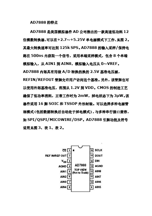
AD7888的特点AD7888是美国模拟器件AD公司推出的一款高速低功耗12位模数转换器,可以在+2.7~+5.25V单电源模式下工作,见图2。
其最大转换速率可达到125k SPS。
AD7888的输入采样/保持电路在500ns内获取一个信号,采用单端采样模式,包含8个单端模拟输入,从AIN1到AIN8,模拟输入电压从0~VREF。
AD7888内部具有用做A/D转换的换的2.5V基准电压源,REFIN/REFOUT管脚允许用户访问这个基准。
另外,该管脚也可以使用外部基准电压,范围从1.2V到VDD。
CMOS的制造工艺确保了低功率消耗,正常工作时为2mW,掉电状态下为3μW。
该器件采用16脚SOIC和TSSOP外形封装。
可以选择多种电源管理模式(包括数据转换后自动处于掉电模式),与多种串行接口兼容,如SPI/QSPI/MICOWIRE/DSP。
AD7888引脚功能及符号说明见图3、表1、表2。
图2AD7888模数转换器图3控制器位功能描述表1AD7888模数转换器管脚表2引脚符号及说明在AD7888中,控制寄存器是8位的只写寄存器。
数据在时钟周期信号的上升沿从AD7888的DIN引脚载入,在此同时获取外部模拟量转换的结果。
每次数据的传输需要准备16个连续时钟信号。
数据只能在片选信号下降沿之后的前8个时钟脉冲的上升沿装入控制寄存器。
串行接口:在图4中显示了详细的串行接口时序图,串行时钟提供了转换时序,且控制AD7888转换信息的输入输出。
CS初始化数据传送和转换处理。
在其下降沿之后的1.5个时钟周期开始采样输入信号,这段时间表示为tACQ(获取时间)。
这是从DIN输出到控制寄存器的MSB位为DONTC一个原因。
在自动关断模式下获取时间必须要虑及5μs的唤醒时间。
整个转换过程还需要14.5个时钟周期来完成。
上升沿之后,总线返回高阻状态。
如果继续保持低电平,则准备新一轮的转换。
进行采样的输入通道的选择是提前写入控制寄存器的,因此在转换时,用户必须提前写入以备通道的转换。

16-, 14-, 12-Bit, 6通道同步采样模数转换器ADS8556/7/8系列包括6个16-, 14-和12-bit模数转换器(ADCs),各自基于连续逼近寄存器原理。
构架是基于充电分配原理,具有一个采样保持功能。
6个模拟输入组成3个通道组。
这些通道组可以并行采样,保留了信号的相对相位信息。
独立的转换开始信号可以控制每个通道的转换,可以是4个通道或者是6个通道一起转换。
器件支持单端,差分模拟输入信号,范围可以是±4VREF或者±2VREF ,最大输入电压可以达到±12V。
器件提供了一个内部的2.5V/3V参考电压源,配合一个10-bit的DA转换器,可以提供2.44mV或2.93mV的步进调整电压。
ADS8556/7/8同样提供一个可选择的并行或串行接口,可以用在硬件模式或软件模式中模拟部分本节讲述模拟输入电路,ADC以及控制信号,以及器件的参考设计模拟输入输入和转换器可以是单端或差分类型,绝对电压范围可以通过使用RANGE引脚进行配置(硬件模式)或控制寄存器(CR)中的RANGE_x位设置为±4V REF或±2V REF。
当使用的参考电压为2.5V时(CR bit C18 = 0),输入电压范围可以是±10V或±5V;当使用的参考电压为3V (CR bit C18 = 1),输入电压范围可以是±12V或±6V。
RANGE引脚在BUSY(如果CR bit C20 = 0)的下降沿锁存。
模拟输入端的输入电流取决于采样率,输入电压和信号的源阻抗。
实质上,模拟输入端的电流仅在采样周期(t ACQ)为内部的电容阵列进行充电。
在最大速率下(280ns),模拟输入电压的源必须能够为10pF的输入电容(±4V REF)或20pF(±2V REF)的输入电容充电。
在转换周期中,没有输入电流,输入阻抗大于1MΩ。

关于LM7806详细中文资料目录1.lm7806介绍2.实际应用3.引脚序号、引脚功能4.lm7806应用电路5.7806电参数三端稳压集成电路lm7806。
电子产品中,常见的三端稳压集成电路有正电压输出的lm78 ×× 系列和负电压输出的lm79××系列。
顾名思义,三端IC是指这种稳压用的集成电路,只有三条引脚输出,分别是输入端、接地端和输出端。
它的样子象是普通的三极管,TO- 220 的标准封装,也有lm9013样子的TO-92封装。
1.lm7806介绍用lm78/lm79系列三端稳压I C来组成稳压电源所需的外围元件极少,电路内部还有过流、过热及调整管的保护电路,使用起来可靠、方便,而且价格便宜。
该系列集成稳压IC型号中的lm78或lm79后面的数字代表该三端集成稳压电路的输出电压,如lm7806表示输出电压为正6V,lm7909表示输出电压为负9V。
因为三端固定集成稳压电路的使用方便,电子制作中经常采用。
最大输出电流1.5A,LM78XX系列输出电压分别为5V;6V;8V;9V;10V;12V;15V;18V;24V。
2.实际应用在实际应用中,应在三端集成稳压电路上安装足够大的散热器(当然小功率7806IC内部电路图.的条件下不用)。
当稳压管温度过高时,稳压性能将变差,甚至损坏。
当制作中需要一个能输出1.5A以上电流的稳压电源,通常采用几块三端稳压电路并联起来,使其最大输出电流为N个1.5A,但应用时需注意:并联使用的集成稳压电路应采用同一厂家、同一批号的产品,以保证参数的一致。
另外在输出电流上留有一定的余量,以避免个别集成稳压电路失效时导致其他电路的连锁烧毁。
在lm78** 、lm79 ** 系列三端稳压器中最常应用的是TO-220 和TO-202 两种封装。

多通道模数转换芯片ADS7956的原理及应用作者:王晓君曹光耀王星来源:《电脑知识与技术》2018年第34期摘要:ADS7956是美国TI公司推出的一款多通道高精度的A/D转换芯片,它采用的是电压输入、逻辑控制、SPI数据串行输出,并具有多通道采集,分辨率高,功耗低,速度快,性能也十分稳定等特点。
首先简要介绍了该芯片ADS7956的性能特点和结构,然后重点分析了串口逻辑时序,讨论了可以设定的三种工作模式,最后给出了该芯片一般的电路应用和部分编程代码,希望在今后的开发应用中,可以对相关的专业人士有一定的指导作用。
关键词:模数转换;多通道;ADS7956;SPI串行输出中图分类号:TN79+2; ; ; ; 文献标识码:A; ; ; ; 文章编号:1009-3044(2018)34-0227-03高性能多通道的模数转换芯片被广泛应用于通信、计算机和医疗设备等领域,对国民经济、国防建设以及科学研究具有重要意义。
一些特定设备需要同时采集多路信号,并且对信号处理的实时性要求非常高,于是分辨率高、通道数多、可靠性能高、低功耗、响应快的AD芯片越来越受到关注和应用。
1 性能特点ADS79XX是TI(德州仪器)公司制造的多通道高精度的A/D转换芯片系列。
而ADS7956是其中一款单5V供电,12通道的A/D转换芯片,是通道数最多的一种。
它采用了成熟的CMOS制作工艺,电容性的再区分设计方法,在模拟输入端有一个电容阵列,使得这种SAR模数转换器时间延迟较短,可以满足DSP,MCU,FPGA等系统的快速性要求,具有很好的实时性。
ADS7956拥有10bit的采样分辨率;47MHz的输入带宽和20MHZ的串行通信速率;最低有效位稳定至1LSB;输入电压信号的最大值取决于外部参考电压REFP,可以选择外接一个电压源,它的范围为2.7~5.25V;持续工作时典型功耗为14.5mW;具有超宽的工作温度范围:-40~+125°C。
AD7862特点:两个快速12-bit ADC,4输入通道,同时取样和转化,4 us吞吐时间,单电源供电,可选的输入电压范围:+10V AD7862-10;+2.5V AD7862-3;0-2.5V AD7862-2。
高速并行接口,低能耗 60mW,省电模式 50uW,对模拟输入有过电压保护,与14位的升级AD(AD7863)兼容。
应用:AC电动机控制,连续电压供应,数据采集系统,通信。
简要描述:AD7862是一个高速,低功耗,双12位的A/D转换,单+5V供电。
它包含两个4us的延时的ADC,两个锁存器,一个内部的+2.5V参考电压和一个高速并行输出端口。
有四个模拟输入通道,分为两组,由A0选择。
每一组通道有两个输入(VA1 & VA2 or VB1 & VB2),它们能同时的被采样和转化,保存相对的信号信息。
它可以接受+10v的输入电压范围(AD7862-10),+2.5(AD7862-3)和0-2.5v(AD7862-2)。
对模拟电压输入,具有过电保护功能,相对地,允许输入电压到达+17v,+7v,+7v,而不会造成损害。
一个单独的转换开始信号(/convst),同时连接在两个锁存器上,可以同时对两路信号开始转化。
BUSY信号,表明转换结束。
这时,两个通道的转换结果可以读出。
在转换完后的第一个读的结果是VA1或VA2通道的数据,第二个读的结果是VA2或VB2通道的数据。
这由选择信号A0是低或高来决定。
当/CS和/RD信号有效时,数据从一个12位的并行数据总线读出。
它遵循传统的dc精确度规定,例如线性,满量程,偏移误差。
它同样还有动态的性能参数,包括谐波失真和信号噪声比率。
AD7862功能模块图ad7862由模拟器件构成,与coms工艺兼容。
在低电压cmos逻辑双极性电路中,这种混合的技术联合使得它更加精确。
它时28脚封装,DIP,SSOP,SOIC。
产品介绍:1.AD7862的特点是有两个ADC功能,允许同时采样和转化两个通道的模拟量。
DESCRIPTIONThe ADS7816 is a 12-bit, 200kHz sampling analogto-digital converter. It features low power operationwith automatic power down, a synchronous serialinterface, and a differential input. The reference voltage can be varied from 100mV to 5V, with a corresponding resolution from 24µV to 1.22mV.Low power, automatic power down, and small sizemake the ADS7816 ideal for battery operated systemsor for systems where a large number of signals must beacquired simultaneously. It is also ideal for remoteand/or isolated data acquisition. The ADS7816 isavailable in an 8-pin plastic mini-DIP, an 8-lead SOIC,or an 8-lead MSOP package.12-Bit High Speed Micro Power SamplingANALOG-TO-DIGITAL CONVERTER®©1996 Burr-Brown Corporation PDS-1355B Printed in U.S.A., March, 1997International Airport Industrial Park • Mailing Address: PO Box 11400, Tucson, AZ 85734 • Street Address: 6730 S. Tucson Blvd., Tucson, AZ 85706 • Tel: (520) 746-1111 • Twx: 910-952-1111Internet: / • FAXLine: (800) 548-6133 (US/Canada Only) • Cable: BBRCORP • Telex: 066-6491 • FAX: (520) 889-1510 • Immediate Product Info: (800) 548-6132FEATURES●200kHz SAMPLING RA TE●MICRO POWER:1.9mW at 200kHz150µW at 12.5kHz●POWER DOWN: 3µA Max●8-PIN MINI-DIP, SOIC, AND MSOP●DIFFERENTIAL INPUT●SERIAL INTERFACEAPPLICATIONS●BATTERY OPERATED SYSTEMS●REMOTE DATA ACQUISITION●ISOLATED DATA ACQUISITIONSAR ControlSerialInterfaceDOUTS/H Amp ComparatorDCLOCK+InVREF–InCDACOPA658ADS7816ADS7816SBAS0612®ADS7816SPECIFICATIONSAt –40°C to +85°C, +VCC = +5V, VREF= +5V, fSAMPLE= 200kHz, fCLK= 16 • fSAMPLE, unless otherwise specified.ADS7816 ADS7816B ADS7816CPARAMETER CONDITIONS MIN TYP MAX MIN TYP MAX MIN TYP MAX UNITS ANALOG INPUTFull-Scale Input Span +In – (–In) 0 VREF ✻✻✻✻VAbsolute Input Voltage +In –0.2 VCC+0.2 ✻✻✻✻V–In –0.2 +0.2 ✻✻✻✻VCapacitance 25 ✻✻pFLeakage Current ±1 ✻✻µASYSTEM PERFORMANCEResolution 12 ✻✻BitsNo Missing Codes 11 12 ✻BitsIntegral Linearity Error ±0.5 ±2 ±0.5 ±2 ±0.5 ±1 LSB(1)Differential Linearity Error ±0.5 ±2 ±0.5 ±1 ±0.25 ±0.75 LSBOffset Error ±4 ✻✻LSBGain Error ±4 ✻✻LSBNoise 33 ✻✻µVrmsPower Supply Rejection 82 ✻✻dBSAMPLING DYNAMICSConversion Time 12 ✻✻Clk CyclesAcquisition Time 1.5 ✻✻Clk CyclesThroughput Rate 200 ✻✻kHzDYNAMIC CHARACTERISTICSTotal Harmonic Distortion VIN= 5.0Vp-p at 1kHz –84 ✻✻dBVIN= 5.0Vp-p at 5kHz –82 ✻✻dBSINAD VIN= 5.0Vp-p at 1kHz 72 ✻✻dBSpurious Free Dynamic Range VIN= 5.0Vp-p at 1kHz 86 ✻✻dBREFERENCE INPUTV oltage Range 0.1 5 ✻✻✻✻VResistance CS = GND, fSAMPLE = 0Hz 5 ✻✻GΩCS = VCC 5 ✻✻GΩCurrent Drain At Code 710h 38 100 ✻✻✻✻µA fSAMPLE= 12.5kHz 2.4 20 ✻✻✻✻µACS = VCC 0.001 3 ✻✻✻✻µADIGITAL INPUT/OUTPUTLogic Family CMOS ✻✻Logic Levels:VIH IIH = +5µA 3 +VCC+0.3 ✻✻✻✻VVILIIL= +5µA –0.3 0.8 ✻✻✻✻VVOH IOH = –250µA 3.5 ✻✻VVOLIOL= 250µA 0.4 ✻✻VData Format Straight Binary ✻✻POWER SUPPL Y REQUIREMENTSVCC Specified Performance 4.50 5.25 ✻✻✻✻V Quiescent Current 380 700 ✻✻✻✻µA fSAMPLE= 12.5kHz(2, 3)30 ✻✻µAfSAMPLE= 12.5kHz(3)280 400 ✻✻µAPower Down CS = VCC, fSAMPLE= 0Hz 3 ✻✻µATEMPERATURE RANGESpecified Performance –40 +85 ✻✻✻✻°C✻Specifications same as grade to the left.NOTE: (1) LSB means Least Significant Bit, with VREFequal to +5V, one LSB is 1.22mV. (2) fCLK= 3.2MHz, CS = VCC for 251 clock cycles out of every 256. (3) Seethe Power Dissipation section for more information regarding lower sample rates.3®ADS7816The information provided herein is believed to be reliable; however, BURR-BROWN assumes no responsibility for inaccuracies or omissions. BURR-BROWNassumes no responsibility for the use of this information, and all use of such information shall be entirely at the user’s own risk. Prices and specifications are subjectto change without notice. No patent rights or licenses to any of the circuits described herein are implied or granted to any third party. BURR-BROWN does notauthorize or warrant any BURR-BROWN product for use in life support devices and/or systems. ELECTROSTATICDISCHARGE SENSITIVITYElectrostatic discharge can cause damage ranging from performance degradation to complete device failure. BurrBrown Corporation recommends that all integrated circuitsbe handled and stored using appropriate ESD protectionmethods.ESD damage can range from subtle performance degradation to complete device failure. Precision integrated circuitsmay be more susceptible to damage because very smallparametric changes could cause the device not to meetpublished specifications.ABSOLUTE MAXIMUM RATINGS(1)+VCC ..................................................................................................... +6VAnalog Input ........................................................... –0.3V to (+VCC + 0.3V)Logic Input ............................................................. –0.3V to (+VCC + 0.3V)Case Temperature ......................................................................... +100°CJunction Temperature .................................................................... +150°CStorage Temperature ..................................................................... +125°CExternal Reference V oltage .............................................................. +5.5VNOTE: (1) Stresses above these ratings may permanently damage the device.PIN CONFIGURATIONPIN ASSIGNMENTSPIN NAME DESCRIPTION1 VREF Reference Input.2 +In Non Inverting Input.3 –In Inverting Input. Connect to ground or to remote ground sense point.4 GND Ground.5 CS/SHDN Chip Select when LOW, Shutdown Mode when HIGH.6 DOUTThe serial output data word is comprised of 12 bits of data. In operation the data is valid on the falling edge of DCLOCK. Thesecond clock pulse after the falling edge of CS enables the serial output. After one null bit the data is valid for the next 12 edges.7 DCLOCK Data Clock synchronizes the serial data transfer and determines conversion speed.8 +VCC Power Supply.PACKAGE/ORDERING INFORMATIONMAXIMUM MAXIMUMINTEGRAL DIFFERENTIAL PACKAGELINEARITY ERROR LINEARITY ERROR TEMPERA TURE DRAWINGPRODUCT (LSB) (LSB) RANGE PACKAGE NUMBER(1)ADS7816P ±2 ±2 –40°C to +85°C Plastic DIP 006ADS7816U ±2 ±2 –40°C to +85°C SOIC 182ADS7816E ±2 ±2 –40°C to +85°C MSOP 337ADS7816PB ±2 ±1 –40°C to +85°C Plastic DIP 006ADS7816UB ±2 ±1 –40°C to +85°C SOIC 182ADS7816EB ±2 ±1 –40°C to +85°C MSOP 337ADS7816PC ±1 ±0.75 –40°C to +85°C Plastic DIP 006ADS7816UC ±1 ±0.75 –40°C to +85°C SOIC 182ADS7816EC ±1 ±0.75 –40°C to +85°C MSOP 337NOTE: (1) For detailed drawing and dimension table, please see end of data sheet, or Appendix C of Burr-Brown IC Data Book.12348765+VCCDCLOCKDOUTCS/SHDNVREF+In–InGNDADS78168-Pin PDIP,8-Lead SOIC,8-Lead MSOP4®ADS7816TYPICAL PERFORMANCE CURVESAt TA = +25°C, VCC = +5V, VREF = +5V, fSAMPLE = 200kHz, and fCLK = 16 • fSAMPLE, unless otherwise specified.CHANGE IN OFFSET vs REFERENCE VOLTAGE54.543.532.521.510.5Change in Offset (LSB)1 2 3 4 5Reference Voltage (V)CHANGE IN OFFSET vs TEMPERATURE0.60.40.2–0.2–0.4–0.6Delta from 25°C (LSB)–55 –40 –25 0 25 70 85Temperature (°C)CHANGE IN GAIN vs REFERENCE VOLTAGE 43.532.521.510.5Change in Gain (LSB)1 2 3 4 5Reference Voltage (V)CHANGE IN GAIN vs TEMPERA TURE0.150.10.05–0.05–0.1–0.15Delta from 25°C (LSB)–55 –40 –25 0 25 70 85Temperature (°C)EFFECTIVE NUMBER OF BITSvs REFERENCE VOLTAGE1211.7511.511.251110.7510.510.2510Effective Number of Bits (rms)0.1 1 10Reference Voltage (V)PEAK-TO-PEAK NOISE vs REFERENCE VOLTAGE 10987654321Peak-to-Peak Noise (LSB)0.1 1 10Reference Voltage (V)5®ADS7816SIGNAL-TO-(NOISE + DISTORTION) vs INPUT LEVEL 8070605040302010Signal-to-(Noise Ratio Plus Distortion) (dB)–40 –35 –30 –25 –20 –15 –10 –5 0Input Level (dB)SIGNAL-TO-(NOISE + DISTORTION) vs FREQUENCY 100908070605040302010Signal-to-(Noise + Distortion) (dB)1 10 100Frequency (kHz)TYPICAL PERFORMANCE CURVES (CONT)At TA = +25°C, VCC = +5V, VREF = +5V, fSAMPLE = 200kHz, and fCLK = 16 • fSAMPLE, unless otherwise specified.POWER SUPPL Y REJECTION vs RIPPLE FREQUENCY–10–20–30–40–50–60–70–80–90Power Supply Rejection (dB)1 10 100 1000 10000Ripple Frequency (kHz)TOTAL HARMONIC DISTORTION vs FREQUENCY–10–20–30–40–50–60–70–80–90–100Total Harmonic Distortion (dB) 1 10 100Frequency (kHz) FREQUENCY SPECTRUM(2048 Point FFT; fIN= 9.9kHz, –0.5dB)–10–20–30–40–50–60–70–80–90–100–110–120Amplitude (dB)0 25 50 75 100Frequency (kHz)SPURIOUS FREE DYNAMIC RANGE andSIGNAL-TO-NOISE RA TIO vs FREQUENCY100908070605040302010Spurious Free Dynamic Rangeand Signal-to-Noise Ratio (dB)1 10 100Frequency (kHz)Spurious Free Dynamic RangeSignal-to-Noise Ratio6®ADS7816TYPICAL PERFORMANCE CURVES (CONT)At TA = +25°C, VCC = +5V, VREF = +5V, fSAMPLE = 200kHz, and fCLK = 16 • fSAMPLE,unless otherwise specified.INTEGRAL LINEARITY ERROR vs CODE1.000.750.500.250.00–0.25–0.50–0.75–1.00Integral Linearity Error (LSB)0 2048 4095CodeDIFFERENTIAL LINEARITY ERROR vs CODE1.000.750.500.250.00–0.25–0.50–0.75–1.00Differential Linearity Error (LSB)0 2048 4095CodeCHANGE IN INTEGRAL LINEARITY AND DIFFERENTIALLINEARITY vs REFERENCE VOLTAGE0.100.050.00–0.05–0.10–0.15–0.20Delta from +5V Reference (LSB)1 2 3 4 5Reference Voltage (V)Change in DifferentialLinearity (LSB)Change in IntegralLinearity (LSB)INPUT LEAKAGE CURRENT vs TEMPERATURE 1010.10.01Leakage Current (nA)–55 –40 –25 0 25 70 85Temperature (°C)SUPPL Y CURRENT vs TEMPERA TURE450400350300250200150Supply Current (µA)–55 –40 –25 0 25 70 85Temperature (°C)fSAMPLE= 12.5kHzfSAMPLE= 200kHzPOWER DOWN SUPPL Y CURRENTvs TEMPERATURE32.521.510.5Supply Current (µA)–55 –40 –25 0 25 70 85Temperature (°C)7®ADS7816TYPICAL PERFORMANCE CURVES (CONT)At TA = +25°C, VCC = +5V, VREF = +5V, fSAMP LE = 200kHz, and fCLK = 16 • fSAMPLE, unless otherwise specified.CHANGE IN INTEGRAL LINEARITY and DIFFERENTIALLINEARITY vs SAMPLE RATE1.51.00.5–0.5Delta from fSAMPLE= 200kHz (LSB)0 100 200 300 400 500Sample Rate (kHz)Change in IntegralLinearity (LSB)Change in DifferentialLinearity (LSB)REFERENCE CURRENT vs TEMPERA TURE(Code = 710h)55504540353025Reference Current (µA)–55 –40 –25 0 25 70 85Temperature (°C)REFERENCE CURRENT vs SAMPLE RA TE(Code = 710h)4035302515105Reference Current (µA)0 40 80 120 160 200Sample Rate (kHz)8®ADS7816THEORY OF OPERA TIONThe ADS7816 is a classic successive approximation register(SAR) analog-to-digital (A/D) converter. The architecture isbased on capacitive redistribution which inherently includesa sample/hold function. The converter is fabricated on a 0.6µCMOS process. The architecture and process allow theADS7816 to acquire and convert an analog signal at up to200,000 conversions per second while consuming very littlepower.The ADS7816 requires an external reference, an externalclock, and a single +5V power source. The external reference can be any voltage between 100mV and VCC. The valueof the reference voltage directly sets the range of the analoginput. The reference input current depends on the conversionrate of the ADS7816.The external clock can vary between 10kHz (625Hz throughput) and 3.2MHz (200kHz throughput). The duty cycle ofthe clock is essentially unimportant as long as the minimumhigh and low times are at least 150ns. The minimum clockfrequency is set by the leakage on the capacitors internal tothe ADS7816.The analog input is provided to two input pins: +In and –In.When a conversion is initiated, the differential input on thesepins is sampled on the internal capacitor array. While aconversion is in progress, both inputs are disconnected fromany internal function.The digital result of the conversion is clocked out by theDCLOCK input and is provided serially, most significant bitfirst, on the DOUTpin. The digital data that is provided on theDOUTpin is for the conversion currently in progress—thereis no pipeline delay. It is possible to continue to clock theADS7816 after the conversion is complete and to obtain theserial data least significant bit first. See the Digital Interfacesection for more information.ANALOG INPUTThe +In and –In input pins allow for a differential input signal.Unlike some converters of this type, the –In input is not resampled later in the conversion cycle. When the convertergoes into the hold mode, the voltage difference between +Inand –In is captured on the internal capacitor array.The range of the –In input is limited to ±200mV. Because ofthis, the differential input can be used to reject only smallsignals that are common to both inputs. Thus, the –In inputis best used to sense a remote signal ground that may moveslightly with respect to the local ground potential.The input current on the analog inputs depends on a numberof factors: sample rate, input voltage, source impedance, andpower down mode. Essentially, the current into the ADS7816charges the internal capacitor array during the sample period. After this capacitance has been fully charged, there isno further input current. The source of the analog inputvoltage must be able to charge the input capacitance (25pF)to a 12-bit settling level within 1.5 clock cycles. When theconverter goes into the hold mode or while it is in the powerdown mode, the input impedance is greater than 1GΩ.Care must be taken regarding the absolute analog inputvoltage. To maintain the linearity of the converter, the –Ininput should not exceed GND ±200mV. The +In inputshould always remain within the range of GND –200mV toVCC+200mV. Outside of these rang es, the converter’s linearity may not meet specifications. REFERENCE INPUTThe external reference sets the analog input range. TheADS7816 will operate with a reference in the range of 100mVto VCC. There are several important implications of this.As the reference voltage is reduced, the analog voltageweight of each digital output code is reduced. This is oftenreferred to as the LSB (least significant bit) size and is equalto the reference voltage divided by 4096. This means thatany offset or gain error inherent in the A/D converter willappear to increase, in terms of LSB size, as the referencevoltage is reduced. The typical performance curves of“Change in Offset vs Reference V oltage‖ and ―Change inGain vs Reference V oltage‖ provide more information.The noise inherent in the converter will also appear toincrease with lower LSB size. With a 5V reference, theinternal noise of the converter typically contributes only0.16 LSB peak-to-peak of potential error to the output code.When the external reference is 100mV, the potential error contribution from the internal noise will be 50 times larger—8 LSBs. The errors due to the internal noise are gaussian innature and can be reduced by averaging consecutive conversion results. For more information regarding noise, consult the typical performance curves ―Effective Number of Bits vs ReferenceV oltage‖ and ―Peak-to-Peak Noise vs Reference V oltage.‖The effective number of bits (ENOB) figure is calculatedbased on the converter’s signal-to-(noise + distortion) ratiowith a 1kHz, 0dB input signal. SINAD is related to ENOBas follows: SINAD = 6.02 • ENOB +1.76.With lower reference voltages, extra care should be taken toprovide a clean layout including adequate bypassing, a cleanpower supply, a low-noise reference, and a low-noise inputsignal. Because the LSB size is lower, the converter will alsobe more sensitive to external sources of error such as nearbydigital signals and electromagnetic interference.The current that must be provided by the external referencewill depend on the conversion result. The current is lowestat full-scale (FFFh) and is typically 25µA at a 200kHzconversion rate (25°C). For the same conditions, the currentwill increase as the input approaches zero, reaching 50µA atan output result of 000h. The current does not increaselinearly, but depends, to some degree, on the bit pattern ofthe digital output.9®ADS7816SYMBOL DESCRIPTION MIN TYP MAX UNITStSMPL Analog Input Sample TIme 1.5 2.0 Clk CyclestCONV Conversion Time 12 Clk CyclestCYC Throughput Rate 200 kHztCSD CS Falling to 0 nsDCLOCK LOWtSUCS CS Falling to 30 nsDCLOCK RisingthDO DCLOCK Falling to 15 nsCurrent DOUTNot ValidtdDO DCLOCK Falling to Next 85 150 nsDOUT Validtdis CS Rising to DOUTTri-State 25 50 nsten DCLOCK Falling to DOUT50 100 nsEnabledtf DOUTFall Time 70 100 nstr DOUT Rise Time 60 100 nsvalue for one clock period. For the next 12 DCLOCKperiods, DOUTwill output the conversion result, most significant bit first. After the least significant bit (B0) has beenoutput, subsequent clocks will repeat the output data but ina least significant bit first format.After the most significant bit (B11) has been repeated, DOUTwill tri-state. Subsequent clocks will have no effect on theconverter. A new conversion is initiated only when CS hasbeen taken HIGH and returned LOW.The reference current diminishes directly with both conversion rate and reference voltage. As the current from thereference is drawn on each bit decision, clocking the converter more quickly during a given conversion period willnot reduce the overall current drain from the reference. Thereference current changes only slightly with temperature.See the curves, ―Reference Current vs Sample Rate‖ and“Reference Current vs Temperatur e‖ in the Typical Performance Curves section for more information.DIGITAL INTERFACESERIAL INTERFACEThe ADS7816 communicates with microprocessors and otherdigital systems via a synchronous 3-wire serial interface asshown in Figure 1 and Table I. The DCLOCK signalsynchronizes the data transfer with each bit being transmitted on the falling edge of DCLOCK. Most receiving systemswill capture the bitstream on the rising edge of DCLOCK.However, if the minimum hold time for DOUTis acceptable,the system can use the falling edge of DCLOCK to captureeach bit.A falling CS signal initiates the conversion and data transfer.The first 1.5 to 2.0 clock periods of the conversion cycle areused to sample the input signal. After the second fallingDCLOCK edge, DOUTis enabled and will output a LOWFIGURE 1. ADS7816 Basic Timing Diagrams.TABLE I. Timing Specifications –40°C to +85°C.CS/SHDNDOUTDCLOCKtDA TAtSUCStCSDtCYCtCONVPOWERDOWNtSMPLNote: (1) After completing the data transfer, if further clocks are applied with CS LOW, the ADC will output LSB-First data then followed with zeroes indefinitely. B11(MSB)B10 B9 B8 B7 B6 B5 B4 B3 B2 B1 B0(1)NULLHI-Z BIT HI-ZB11 B10 B9 B8NULLBITCS/SHDNDOUTDCLOCKtCONVtDA TAtSUCStCYCPOWER DOWNtSMPLNote: (2) After completing the data transfer, if further clocks are applied with CSLOW, the ADC will output zeroes indefinitely.tDA TA: During this time, the bias current and the comparator power down and the reference inputbecomes a high impedance node, leaving the CLK running to clock out LSB-First data or zeroes. B11(MSB)B10 B9 B8 B7 B6 B5 B4 B4 B3 B3 B2 B2 B1 B1 B0NULLHI-Z BIT HI-ZB5 B6 B7 B8 B9 B10 B11(2)tCSD10®ADS7816DOUT1.4VTest Point3kΩ100pFCLOADtrDOUTVOHVOLtftdDOthDODOUTDCLOCKVOHVOLVILDOUTtdisWaveform 2, tentdisWaveform 1100pFCLOAD3kΩtdisCS/SHDNDOUTWaveform 1(1)DOUTWaveform 2(2)90%10%VIH1B112tenCS/SHDNDCLOCKDVOLOUTVCCLoad Circuit for tdDO, tr, and tfV oltage Waveforms for DOUT Rise and Fall TImes tr, and tfV oltage Waveforms for DOUT Delay Times, tdDO Load Circuit for tdisV oltage Waveforms for tenFIGURE 2. Timing Diagrams and Test Circuits for the Parameters in Table I.V oltage Waveforms for tdisDESCRIPTION ANALOG V ALUEFull Scale Range VREFLeast Significant VREF/4096Bit (LSB)Full Scale VREF –1 LSB 1111 1111 1111 FFFMidscale VREF/2 1000 0000 0000 800Midscale – 1 LSB VREF/2 – 1 LSB 0111 1111 1111 7FFZero 0V 0000 0000 0000 000Table II. Ideal Input V oltages and Output Codes.DIGITAL OUTPUT:STRAIGHT BINARYBINARY CODE HEX CODENOTES: (1) Waveform 1 is for an output with internal conditions such thatthe output is HIGH unless disabled by the output control. (2) Waveform 2is for an output with internal conditions such that the output is LOW unlessdisabled by the output control.DA TA FORMA TThe output data from the ADS7816 is in Straight Binaryformat as shown in Table II. This table represents the idealoutput code for the given input voltage and does not includethe effects of offset, gain error, or noise.POWER DISSIPATIONThe architecture of the converter, the semiconductor fabrication process, and a careful design allow the ADS7816 toconvert at up to a 200kHz rate while requiring very littlepower. Still, for the absolute lowest power dissipation, thereare several things to keep in mind.The power dissipation of the ADS7816 scales directly withconversion rate. The first step to achieving the lowest powerdissipation is to find the lowest conversion rate that willsatisfy the requirements of the system.In addition, the ADS7816 is in power down mode under twoconditions: when the conversion is complete and wheneverCS is HIGH (see Figure 1). Ideally, each conversion shouldoccur as quickly as possible, preferably, at a 3.2MHz clockrate. This way, the converter spends the longest possibletime in the power down mode. This is very important as the11®ADS7816converter not only uses power on each DCLOCK transition(as is typical for digital CMOS components) but also usessome current for the analog circuitry, such as the comparator. The analog section dissipates power continuously, untilthe power down mode is entered.Figure 3 shows the current consumption of the ADS7816versus sample rate. For this graph, the converter is clockedat 3.2MHz regardless of the sample rate—CS is HIGH forthe remaining sample period. Figure 4 also shows currentconsumption versus sample rate. However, in this case, theDCLOCK period is 1/16th of the sample period—CS isHIGH for one DCLOCK cycle out of every 16.There is an important distinction between the power downmode that is entered after a conversion is complete and thefull power down mode which is enabled when CS is HIGH.While both power down the analog section, the digital sectionis powered down only when CS is HIGH. Thus, if CS is leftLOW at the end of a conversion and the converter is continually clocked, the power consumption will not be as low aswhen CS is HIGH. See Figure 5 for more information.By lowering the reference voltage, the ADS7816 requiresless current to completely charge its internal capacitors onboth the analog input and the reference input. This reductionin power dissipation should be weighed carefully against theresulting increase in noise, offset, and gain error as outlinedin the Reference section. The power dissipation of theADS7816 is reduced roughly 10% when the reference voltage and input range are changed from 5V to 100mV.SHORT CYCLINGAnother way of saving power is to utilize the CS signal toshort cycle the conversion. Because the ADS7816 places thelatest data bit on the DOUTline as it is generated, theconverter can easily be short cycled. This term means thatthe conversion can be terminated at any time. For example,if only 8-bits of the conversion result are needed, then theconversion can be terminated (by pulling CS HIGH) afterthe 8th bit has been clocked out.This technique can be used to lower the power dissipation(or to increase the conversion rate) in those applicationswhere an analog signal is being monitored until some condition becomes true. For example, if the signal is outside apredetermined range, the full 12-bit conversion result may not be needed. If so, the conversion can be terminated after the first n-bits, where n might be as low as 3 or 4. This results in lower power dissipation in both the converter and the rest of the system, as they spend more time in the power down mode.LAYOUTFor optimum performance, care should be taken with the physical layout of the ADS7816 circuitry. This is particularly true if the reference voltage is low and/or the conversion rate is high. At 200kHz conversion rate, the ADS7816 makes a bit decision every 312ns. That is, for each subsequent bit deci- 1000100101Supply Current (µA)1 10 100 1000Sample Rate (kHz)TA= 25°CVCC= VREF= +5VfCLK= 3.2MHzFIGURE 3. Maintaining fCLK at the Highest Possible Rate Allows Supply Current to Drop Directly withSample Rate.1000100101Supply Current (µA)1 10 100 1000Sample Rate (kHz)TA= 25°CVCC= VREF= +5VfCLK= 16 • fSAMPLEFIGURE 4. Scaling fCLK Reduces Supply Current Only Slightly with Sample Rate.FIGURE 5. Shutdown Current is Considerably Lower with CS HIGH than when CS is LOW.605040302010Supply Current (µA)1 10 100 1000Sample Rate (kHz)TA= 25°CVCC= VREF= +5VfCLK= 16 • fSAMPLECS LOW(GND)CS = HIGH (VCC)12®。
HT7886芯片手册集成电路英语:integrated circuit,缩写作 IC;或称微电路(microcircuit)、微芯片(microchip)、晶片/芯片(chip)在电子学中是一种将电路(主要包括半导体设备,也包括被动组件等)小型化的方式,并时常制造在半导体晶圆表面上。
中文名芯片外文名microchip别名微电路、微芯片、集成电路含义半导体元件产品的统称制造设备光刻机快速导航介绍集成电路的发展分类相关政策中国芯片相关新闻简介将电路制造在半导体芯片表面上的集成电路又称薄膜(thin-film)集成电路。
另有一种厚膜(thick-film)集成电路(hybrid integrated circuit)是由独立半导体设备和被动组件,集成到衬底或线路板所构成的小型化电路。
从1949年到1957年,维尔纳·雅各比(Werner Jacobi)、杰弗里·杜默(Jeffrey Dummer)、西德尼·达林顿(Sidney Darlington)、樽井康夫(Yasuo Tarui)都开发了原型,但现代集成电路是由杰克·基尔比在1958年发明的。
其因此荣获2000年诺贝尔物理奖,但同时间也发展出近代实用的集成电路的罗伯特·诺伊斯,却早于1990年就过世。
介绍晶体管发明并大量生产之后,各式固态半导体组件如二极管、晶体管等大量使用,取代了真空管在电路中的功能与角色。
到了20世纪中后期半导体制造技术进步,使得集成电路成为可能。
相对于手工组装电路使用个别的分立电子组件,集成电路可以把很大数量的微晶体管集成到一个小芯片,是一个巨大的进步。
集成电路的规模生产能力,可靠性,电路设计的模块化方法确保了快速采用标准化集成电路代替了设计使用离散晶体管。
集成电路对于离散晶体管有两个主要优势:成本和性能。
成本低是由于芯片把所有的组件通过照相平版技术,作为一个单位印刷,而不是在一个时间只制作一个晶体管。