TP5100中文datasheet
- 格式:pdf
- 大小:657.76 KB
- 文档页数:15
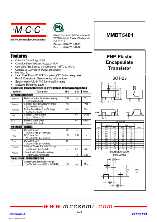
MMBT5401PNP Plastic Encapsulate TransistorFeatures• Collector Current:I CM =0.6A• Collector-Base Voltage:V (BR)CBO =160V• Operating And Storage Temperatures –55O C to 150O C • Capable of 0.3Watts of Power Dissipation • Marking:2LElectrical Characteristics @ 25OC Unless Otherwise SpecifiedSymbol ParameterMin Max Units OFF CHARACTERISTICSV (BR)CEO Coll e ctor -Emitter Breakdown Voltage (I C =1.0m Adc,I B =0)150--- Vdc V (BR)CBO Collector-Base Breakdown Voltage (I C =100uAdc,I E =0)160--- Vdc V (BR)EBO Emitter-Base Breakdown Voltage (I E =10uAdc,I C =0) 5.0--- VdcI CBO Collector Cutoff Current (V CB =120Vdc,I E =0)---0.1uAdcI EBOEmitter Cutoff Current (V EB =4.0Vdc,I C =0)---0.1uAdcON CHARACTERISTICSh FE-1DC Current Gain(V CE =5.0Vdc,I C =1.0mAdc)80------ h FE-2DC Current Gain(V CE =5.0Vdc,I C =10mAdc)100200--- h FE-3DC Current Gain(V CE =5.0Vdc,I C =50mAdc)50------V CE(sat)Collector-Emitter Saturation Voltage (I C =50mAdc,I B =5.0mAdc)---0.5Vdc V BE(sat)Base-Emitter Saturation Voltage (I C =50mAdc,I B =5.0mAdc)---1.0VdcSMALL-SIGNAL CHARACTERISTICSf TCurrent Gain-Bandwidth Product(I C =10mAdc,V CE =5.0Vdc, f=30MHz)100---MHzRevision: A 2011/01/01omp onents 20736Marilla Street Chatsworth! "# $ % ! "#Micro Commercial Componentswww.mccsemi .com1 of 2• Lead Free Finish/RoHS Compliant ("P" Suffix designates RoHS Compliant. See ordering information)• Epoxy meets UL 94 V-0 flammability rating • Moisure Sensitivity Level 1/Revision: A 2011/01/01Micro Commercial Componentswww.mccsemi .com2 of 23Ordering Information :***IMPORTANT NOTICE***Micro Commercial Components Corp. reserve s the right to make changes without further notice to any product herein to make corrections, modifications , enhancements , improvements , or other changes . Micro Commercial Components Corp . does not assume any liability arising out of the application or use of any product described herein; neither does it convey any license under its patent rights ,nor the rights of others . The user of products in such applications shall assume all risks of such use and will agree to hold Micro Commercial Components Corp . and all the companies whose products are represented on our website, harmless against all damages.***LIFE SUPPORT***MCC's products are not authorized for use as critical components in life support devices or systems without the express writtenapproval of Micro Commercial Components Corporation.***CUSTOMER AWARENESS***Counterfeiting of semiconductor parts is a growing problem in the industry. Micro Commercial Components (MCC) is taking strong measures to protect ourselves and our customers from the proliferation of counterfeit parts. MCC strongly encourages customers to purchase MCC parts either directly from MCC or from Authorized MCC Distributors who are listed by country on our web page cited below . Products customers buy either from MCC directly or from Authorized MCC Distributors are genuine parts, have full traceability, meet MCC's quality standards for handling and storage. MCC will not provide any warranty coverage or other assistance for parts bought from Unauthorized Sources. MCC is committed to combat this global problem and encourage our customers to do their part in stopping this practice by buying direct or from authorized distributors.DevicePackingPart Number-T PTape&Reel;3Kpcs/Reel/分销商库存信息: MICRO-COMMERICAL-CO MMBT5401-TP。
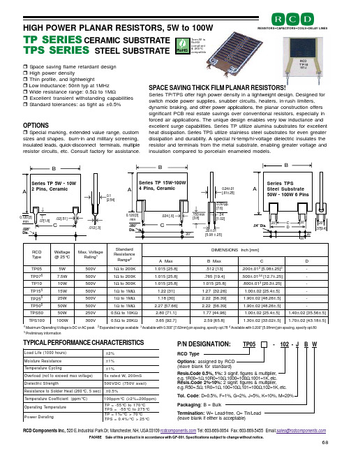
SPACE SAVING THICK FILM PLANAR RESISTORS!Series TP/TPS offer high power density in a lightweight design. Designed for switch mode power supplies, snubber circuits, heaters, in-rush limiters,dynamic braking, and other power applications, the planar construction offers significant PCB real estate savings over conventional resistors, especially in forced air applications. The unique design enables very low inductance and excellent surge capabilities. Series TP utilize alumina substrates for excellent heat dissipation. Series TPS utilize stainless steel substrates for even greater dissipation and durability. A special hi-temp/hi-voltage dielectric insulates the resistor and terminals from the metal substrate, enabling greater voltage and insulation compared to porcelain enameled models.OPTIONSSpecial marking, extended value range, custom sizes and shapes, burn-in and military screening,insulated leads, quick-disconnect terminals, multiple resistor circuits, etc. Consult factory for assistance.HIGH POWER PLANAR RESISTORS, 5W to 100WTP SERIES CERAMIC SUBSTRATE TPS SERIES STEEL SUBSTRATE1 Maximum Operating Voltage is DC or AC peak2 Expanded range available3 Available with 0.300” [7.62mm] pin spacing, specify opt.784 Available with 0.200” [5.08mm] pin spacing, specify opt.80 5Preliminary informationTYPICAL PERFORMANCE CHARACTERISTICSD C R e p y T e g a t t a W C °52@e g a t l o V .x a M g n i t a R 1d r a d n a t Se c n a t s i s e R e g n a R 2]m m [h c n I S N O I S N E M I D x a M A x a M B CD 50P T W 5V 0051ΩK 002o t ]8.52[510.1]31[215.10.±002.3]52.±80.5[3-70P T 5W 5.7V 0051ΩK 002o t ]8.52[510.1]4.91[567.10.±005.4,3]52.±7.21[-01P T W 01V 0051ΩK 003o t ]8.52[510.1]8.52[510.110.±008.3]52.±3.02[-51P T 5W 51V 0051ΩM 1o t Ω]13[22.1]62.23[72.1]5.±4.52[20.±00.1-52P T 5W 52V 0051ΩM 1o t Ω]03[81.1]93.65[22.2]5.±62.84[20.±09.1-05P T 5W 05V 0051ΩM 1o t Ω]66.75[72.2]93.65[22.2]5.±62.84[20.±09.1-05S P T W 05V 0525.0ΩK 01o t Ω]1.17[08.2]69.44[77.1]5.±4.52[20.±00.1]5.±65.53[20.±04.1001S P T W01V0035.0ΩK 02o t Ω]7.29[56.3]8.56[95.2]5.±20.33[20.±03.1]5.±81.34[20.±07.1)s r u o h 0001(e f i L d a o L %2±e c n a t s i s e R e r u t s i o M %1±e T p m e r u t a r e gn i l c y C %1±(d a o l r e v O )e g a t l o v x a m d e e c x e o t t o n S m 002,W d e t a r x 5ht g n e r t S c i r t c e l e i D )l i a v a V 057(C D V 005e c n a t s i s e R )c e s 5,C °062(t a e H r e d l o S o t %5.0±/m p p (t n e i c i f f e o C e r u t a r e p m e T )C °(C °m p p 001≥)m p p 002=%2er u t a r e p m e T g n i t a r e p O C °071o t C °55-=P T C °572o t C °55-=S P T r e w o P gn i t a r e D C °07>C °/%1=P T C°52>C °/%4.0=S P T FA048E Sale of this product is in accordance with GF-061. Specifications subject to change without notice.Space saving flame retardant design High power densityThin profile, and lightweightLow Inductance: 50nh typ at 1MHz Wide resistance range: 0.5Ω to 1M ΩExcellent transient withstanding capabilities Standard tolerances: as tight as ±0.5%.012 [.3]→0.1[2.54]←→ ← ||B|B|||B RCD Components Inc, 520 E.Industrial Park Dr, Manchester, NH, USA 03109 Tel: 603-669-0054 Fax: 603-669-5455 Email:sales@RESISTORS CAPACITOR S C OILS DELAY LINES68P/N DESIGNATION:Termination: W= Lead-free, Q= Tin/Lead (leave blank if either is acceptable)TP05 - 102 - J B WRCD TypePackaging : B = BulkTol. Code : D=0.5%, F=1%, G=2%, J=5%, K=10%, M=20%Options : assigned by RCD (leave blank for standard)Resis.Code 0.5%, 1%: 3 signif. figures & multiplier,e.g. 1R00=1Ω,10R0=10Ω,1000=100Ω,1001=1K, etc.Resis.Code 2%-10%: 2 signif. figures & multiplier,e.g. R50=.5Ω, 1R0=1Ω, 100=10Ω,101=100Ω,102=1K, etc.Term.W is RoHS compliant & 260°C compatible元器件交易网。

菲尼克斯5100说明书菲尼克斯现货FL WLAN 5100 菲尼克斯现货FL WLAN 5100 WLAN接入点/端/中继器MIMO 3x3:2WLAN 02.11a、b、g、n2.4 GHz/5 GHz3根外置天线2x RJ 45尺寸(宽度 x 高度 x 深度)40 mm x 109 mm x 109 mm尺寸说明高度含天线插座,不含天线电缆FL WLAN以太网端口适配器是一款经济型工业WLAN 适配器,可将兼容以太网的设备连接到WLAN网络。
该以太网端口适配器外形紧凑,坚固耐用,内置无线模块和天线。
该设备防护等级达IP65,可直接现场安装,通过带M12连接器的以太网电缆连接到自动化设备。
优势:可直接在集成到应用以太网端口适配器的主要应用领域安装快捷轻松安装在现场以太网端口适配器是一种简易解决方案,可轻松将带以太网接口的工业自动化设备连接到WLAN网络。
该设备防护等级达IP65,可直接现场安装,通过带M12连接器的以太网电缆连接到自动化设备。
优势:内置天线的紧凑型IP65模块用于以太网和电力传输的M12接口轻松安装在现场自动组态,调试更简单安全通过Mode按钮轻松组态使用Mode按钮,无需组态即可轻松快速地构建安全的点到点网络和小型网络。
此外,也可通过网络浏览器轻松组态。
通过AT命令进行高级设置轻松组态和控制FL EPA 2在WLAN EPA模块运行过程中,可通过控制器发出的简单AT命令对其进行自动组态和控制。
这样就可以通过移动系统的控制器根据位置对漫游过程(即接入点之间的转换)进行控制。
FL EPA产品一览特性FL EPA 2FL EPA 2 RSMAWLAN标准IEEE 02.11a/b/gIEEE 02.11 a/b/g频段和道(*依不同国家而定)2.4 GHz,1-11道5 GHz:36-140道(端)5 GHz:36-4道(接入点)2.4 GHz,1-11道5 GHz:36-140道(端)5 GHz:36-4道(接入点)大数据速率(总值)54Mbps54 Mbps大数据流量(净值)< 20 Mbps< 20 Mbps运行模式端(单端网桥、多端网桥)(微型接入点)两个FL EPA模块之间的无线网桥端(单端网桥、多端网桥)(微型接入点)两个FL EPA模块之间的无线网桥大传输功率2.4 GHz:17 dBm(包括天线)5 GHz:15 dBm(包括天线)2.4 GHz:17 dBm(包括天线)5 GHz:15 dBm(包括天线)天线数1(内置)1(外置),RSMA接口安装后的防护等级IP65IP65环境温度(工作)-30°C … 60°C … 65°C电源9 … 30 V DC,大1.7 W9 …30 V DC,大1.7 W特殊性能双无线板:WLAN和蓝牙双无线板:WLAN和蓝牙功能强大的WLAN IEEE 02.11n模块,通范围更广采用新标准和MIMO技术,扩展通范围该设备有*的无线号,并采用符合IEEE 02.11n标准的MIMO(多点输入,多点输出)多天线技术,可在长距离范围内实现稳定、高速且可靠的无线通。

DatasheetEasyPoint TMN50P111Navigation Module1 General DescriptionEasyPoint™ N50P111 is a miniature joystick module concept based on contact-less, magnetic movement detection. The integrated two-dimensional linear encoder monitors the movement of the magnet incorporated in the knob and provides directly the x and ycoordinates via I²C output. An integrated mechanical push button built in the module provides a “select” function.Figure 1. N50P111-xxxxx-H2 Key FeaturesXY coordinates direct read with 8-bit resolution 2.7V to 3.6V operating voltage Down to 1.7V I/O voltageLateral magnet movement radius up to 2.0mm High-speed I²C interfaceConfigurable interrupt output for motion detection Push button feature3 ApplicationsThe EasyPoint™ N50P111 is ideal for small form-factor manual input devices in battery operated equipment, such as Mobile phones, MP3 players, PDAs, GPS receivers, Gaming consoles and Analog joystick replacement.4 BenefitsHigh reliability due to magnetic non-contact sensing Low power consumption Two operating modes-Idle mode-Low Power modeN50P111Push button GNDI²C AddressGND: 0x40VDDp: 0x41AS5013Two-dimensional magnetic encoderContents1 General Description (1)2 Key Features (1)3 Applications (1)4 Benefits (1)5 Pin Assignments (4)5.1 Pin Descriptions (4)6 Absolute Maximum Ratings (5)7 Electrical Characteristics (6)7.1 Operating Conditions (6)7.2 Digital IO Pads DC/AC Characteristics (6)7.3 Switch Characteristics (7)7.4 Mechanical Specifications (8)7.5 Recommended Reflow Temperature Profile (8)8 Using the N50P111 Module (9)8.1 Powering up the Module (9)8.2 Registers Initialization (9)8.3 C Source Code Example (10)8.3.1 Initialization (10)8.3.2 Offset Calibration (10)8.3.3 Dead Zone area (11)8.3.4 Interrupt Routine (11)9 XY Coordinates Interpretation (12)9.1 EasyPoint Operating Principle (12)9.1.1 Knob Displacement and Register Value Relation (13)9.2 Operation Principle (14)10 I²C interface (15)10.1 Interface Operation (15)10.2 I²C Electrical Specification (16)10.3 I²C Timing (17)10.4 I²C Modes (18)10.4.1 Automatic Increment of Address Pointer (18)10.4.2 Invalid Addresses (18)10.4.3 Reading (18)10.4.4 Writing (18)10.4.5 High Speed Mode (21)10.4.6 Automatic Increment of Address Pointer (22)10.4.7 Invalid Addresses (22)10.5 SDA, SCL Input Filters (22)11 I²C Registers (23)11.1 Control Register 1 (0Fh) (23)11.2 X Register (10h) (25)11.3 Y_res_int Register (11h) (25)11.4 Xp Register (12h) (25)11.5 Xn Register (13h) (25)11.6 Yp Register (14h) (26)11.7 Yn Register (15h) (26)11.8 M_ctrl Register (2Bh) (26)11.9 J_ctrl Register (2Ch) (27)11.10 T_ctrl Register (2Dh) (27)11.11 Control Register 2 (2Eh) (27)11.12 Registers Table (28)12 Package Drawings and Markings (30)Datasheet - P i n A s s i g n m e n t s5 Pin Assignments5.1 Pin DescriptionsTable 1. Pin DescriptionsConnector Pin #Pin Type Description 1Power VDDp: IO power supply for SCL, SDA, INTn, 1.7V ~ 3.6V2Power VDD: Core power supply, 2.7V ~ 3.6V3Power GND4Bi-directional SDA: I²C bus data, open drain5Input SCL: I²C bus clock6Input RESETn: Reset input, active LOW0: GND → Reset, all registers return to their reset value 1: VDDp → Normal operation mode7Open drain INTn: Interrupt output, open drain: Active: LOWInactive: Hi-Z8Output SWITCHn: Push button signal output: Not pushed: OpenPushed: GND9Input ADDR: I²C Address selection input:0: GND → 0x401: VDDp → 0x411234J1VDDVDDpSCLSDAGNDDatasheet - A b s o lu t e M a x im u m R a ti n g s6 Absolute Maximum RatingsStresses beyond those listed in Table 2 may cause permanent damage to the device. These are stress ratings only, and functional operation of the device at these or any other conditions beyond those indicated in Electrical Characteristics on page 6 is not implied. Exposure to absolute maximum rating conditions for extended periods may affect device reliability.Table 2. Absolute Maximum RatingsSymbol Parameter Min Max Units NotesV DD DC supply voltage-0.35VVDDp Peripheral supply voltage-0.35VDD + 0.3V SCL, SDA, RESETn, ADDRV IN Input pin voltage -0.3VDDp + 0.3VSCL, SDA, RESETn, ADDR - 3.6VI SCR Input current (latchup immunity)-100100mA Norm: JEDEC 78ESD Electrostatic discharge-±2kV All pins, Norm: MIL 883 E method 3015 T Strg Storage temperature-4085ºCHumidity non-condensing585%Degrees of protection IP5X Norm: IEC 605297 Electrical Characteristics7.1 Operating ConditionsT AMB = -20 to +70ºC, VDD = 3.3V 7.2 Digital IO Pads DC/AC CharacteristicsTable 3. Operating Conditions Symbol ParameterMin TypMax Units NotesVDDCore Supply voltage2.73.6VVDDp Peripheral Supply voltage 1.7VDD VInput: RESETnOpen drain outputs: SCL, SDA, INTn.External I²C pull up resistor to be connected to VDDp.IDD SMaximal average current consumption on VDD,Pulsed peaks = IDD fdepends on the sampling time ts[ms]3+3760/ts [ms]µAT AMB = -20 to +50 ºC10+3760/ts [ms]T AMB = 50 to +70 ºC IDD I Current consumption on core supply, Idle mode,no readout (ts = infinite)3µAT AMB = -20 to +50 ºC10T AMB = 50 to +70 ºC IDD f Current consumption on core supply,Full Power mode 10mA Continuous current pin VDD Maximum sampling ts = 450µs Tpua Power up time analog 1000µs Step on VDD to Data_Ready Tconv Conversion time 450µs Read X/Y coordinate I²C STOP condition to Data_Readyt P,W Nominal wakeup time 20320ms T AMBAmbient temperature range -20+70ºCResolution of XY displacement8Over 2*dx and 2*dy axisTable 4. Digital IO Pads DC/AC Characteristics Symbol ParameterMinMaxUnitsNotesInputs: SCL, SDAV IH High level input voltage 0.7 * VDDpV I²C V IL Low level input voltage 0.3 * VDDpV I²C I LEAK Input leakage current 1µA VDDp = 3.6V Inputs: ADDR, RESETn (JEDEC76)V IH High level input voltage 0.65 * VDDpV JEDEC V IL Low level input voltage 0.35 * VDDpV JEDEC I LEAK Input leakage current1µAVDDp = 3.6VOutputs: SDAV OHHigh level output voltageOpen drainLeakage current 1µA High level outputvoltage7.3 Switch CharacteristicsV OL1Low level output voltageVSS + 0.4V-6mA; VDDP > 2V;fast mode V OL3VDDP * 0.2V-6mA; VDDP ≤ 2V;fast mode V OL1VSS + 0.4V-3mA; VDDP > 2V;high speed V OL3VDDP * 0.2V -3mA; VDDP ≤ 2V;high speed C L Capacitive load 400pF standard mode ( 100 kHz )400pF fast mode ( 400 kHz )100pFhigh speed mode ( 3.4 MHz )Outputs: INTn (JEDEC76)V OH High level output voltage Open drain1µA Leakage current High level output voltageV OL Low level output voltageVSS + 0.2V -100µA VSS + 0.45-2mA C LCapacitive load30pFstandard mode ( 100 kHz )Table 5. Switch CharacteristicsParameterMinMax Units Notes Contact resistance of dome switch 750m ΩNorm: EIA-364-23Dielectric withstanding voltage100Vac Norm: EIA-364-20Insulation resistance 100m ΩNorm: EIA-364-21, 100VdcBouncing (On/Off)5msRate: 2 times/sec.Table 4. Digital IO Pads DC/AC Characteristics Symbol ParameterMinMax Units Notes7.4 Mechanical Specifications7.5 Recommended Reflow Temperature ProfileTable 6. Mechanical SpecificationsParameter Note Number of operating shaftsSingle shaft Shaft material LCP Housing material LCP & PA46Shell material Stainless Steel or Copper alloyTravel (XY operation)±2.00mm (±10%)Travel (Z push operation)0.22mm (±0.05mm)Directional operating force (XY direction)0.70N (±0.15N)Push operating force (Z direction)1.80N (±15%)Vibration10-500-10Hz 15 minutes, 12 cycles, 3 axes (total 36 cycles)Operating life – XY direction Each direction > 1 million cyclesOperating life – Push Z direction > 1 million cyclesShaft strength (XYZ direction)> 3.5 kgfFree fall Dispensing Glue40 drops(2X6 sides + 1X12 edges + 2X8 corners) @ 1.5m drop height to concrete surface, module is assembled to phone mechanics.Over forceDispensing Glue 1.5kgf > 100k cycles8 Using the N50P111 Module8.1 Powering up the ModuleThe N50P111 module has a Power ON Reset (POR) cell to monitor the VDD voltage at startup and reset all the internal registers. After the internal reset is completed, the POR cell is disabled in order to save current during normal operation.If VDD drops below 2.7V down to 0.2V, the POR cell will not be enabled back, and the registers will not be correctly reseted or can get random values.Note:It is highly recommended to control the external RESETn signal by applying a LOW pulse of >100ns once VDD has reached 2.7V and VDDp reached 1.7V.8.2 Registers InitializationAfter Power Up, the following sequence must be performed:1. VDD and VDDp Power up, and reached their nominal values (VDD>2.7V, VDDp>1.7V).2. Initialization:a. RESETn pulse LOW during >100ns, then RESETn HIGHb. Loop check register [0Fh] until the value F0h or F1h is present (reset finished, registers to default values)c. Write value 16h into register [2Dh]3. Perform an Offset Calibration (X and Y coordinate compensation for zero position)4. Configure the Dead Zone Area for Wake-up function (if needed)5. Configure the wanted Power Mode and INT function into register [0Fh] (Idle mode / Low Power Mode with Timebase configuration, INTfor Wake-up or Coordinates ready)6. X Y coordinates are ready to be read.8.3 C Source Code Example8.3.1 Initializationvoid EasyPoint_init (void){unsigned char Reset_status = 0;RESETn = 0;Delay_ms(1);// RESETn pulse after power upRESETn = 1; Delay_ms(1);while (Reset_status != 0xF0)// Check the reset has been done{Reset_status = I2C_Read8(0x40, 0x0F) & 0xFE;}I2C_Write8(0x40, 0x2E, 0x16); // Scaling factor for N50 (2.0mm knob travel) }8.3.2 Offset Calibrationvoid Offset_Calibrate (void){char i;int x_cal=0, y_cal=0;EA = 0;// Disable the MCU interruptsI2C_Write8(0x40, 0x0F, 0x00);// Low Power Mode 20msDelay_ms(1);I2C_Read8(0x40, 0x11); // Flush an unused Y_reg to reset the interruptfor (i=0; i<16; i++)// Read 16 times the coordinates and then average{while (INTn);// Wait until next interrupt (new coordinates)x_cal += (signed char) I2C_Read8(0x40, 0x10); // Read X positiony_cal += (signed char) I2C_Read8(0x40, 0x11); // Read Y position }// offset_X and offset_Y are global variables, used for each coordinate readout in the interrupt routineoffset_X = -(x_cal>>4); // Average X: divide by 16offset_Y = -(y_cal>>4); // Average Y: divide by 16EA = 1; // Enable the MCU interrupts}分销商库存信息: AMSN50P111。
User's GuideSLIU007–September2011TPL0501EVM User GuideContents1Features (2)2Introduction (2)3Mode Selection (2)4Jumper Connections (3)5Software Setup (4)6Operation (4)6.1Voltage Reference Mode (5)6.2Variable Gain Mode (5)7Layouts (7)8Bill of Materials (9)List of Figures1GUI for DPOT Control (4)2TPL0501Variable Gain (5)3TPL0501EVM Schematic (6)4Routing,Assembly and Silkscreen Top (7)5Layer2Ground Plane (7)6Layer3Power Plane (8)7Routing and Assembly Bottom (8)List of Tables1Description of Connectors and Jumpers (3)2430Boost-TPL0501EVM Bill of Material(DPOT Only) (9)Windows is a trademark of Microsoft Corporation.1 SLIU007–September2011TPL0501EVM User GuideSubmit Documentation FeedbackCopyright©2011,Texas Instruments Incorporated/Features 1Features•Works with low cost MSP430based LaunchPad platform•Simple GUI to control EVM•EVM can be operate two different modes–Adjustable Voltage reference mode–Variable gain mode•Board is entirely powered by USB2IntroductionThe TPL0501is a single channel,linear-taper digital potentiometer with256wiper positions.This devicecan be used as a three-terminal potentiometer or as a two-terminal rheostat.The TPL0501has an end–to-end resistance of100kΩ.The internal registers of the TPL0501can be accessed using aSPI-compatible interface.The TPL0501has a nominal temperature coefficient of35ppm/°C.The TPL0501is available in an8-pin SOT-23and8-microQFN package with a specified temperature range of–40°C to125°C.The TPL0501EVM is designed to operate with the Texas Instruments LaunchPad(MSP-EXP430G2).TheTPL0501EVM come with a preprogrammed MSP430G2553microcontroller which is to be inserted in theDIP socket on the LaunchPad.The LaunchPad can be separately purchased at /launchpad.The TPL0501EVM has two different evaluation modes:Mode1–Adjustable voltage reference mode–in this mode the TPL0501is used in conjunction with anLMV321op amp as an adjustable voltage reference circuit.Mode2–Variable gain mode–in this mode the TPL0501is configured as part of a variable gainnon-inverting amplifier.The gain of the amplifier can be controlled by a digital interface.This mode can beused to evaluate the bandwidth of the TPL0501.The EVM is operated by connecting the LaunchPad to a PC that has Windows™()via the USBPort.Other standard lab equipment such as Signal generator,multimeter,spectrum analyzer etc may berequired for detailed analysis of the TPL0501performance using this EVM.3Mode SelectionTo setup any of these two modes,begin by connecting the EVM to the LaunchPad.Note the location ofthe VCC and GND pins on headers J1and J2on both the LaunchPad and the EVM to ensure correctinstallation.1.Voltage reference modeConnect pins1and2of Jumper J7.Connect pins1and2of Jumper J5.Connect the LaunchPad and TPL0501EVM to a computer through the USB connector.2.Variable Gain modeConnect pins2and3of jumper J6.Connect pins1and2of jumper J7.Attach a signal generator to the EXT_IN connector.Connect the LaunchPad and TPL0501EVM to a computer through the USB connector 2TPL0501EVM User Guide SLIU007–September2011Submit Documentation FeedbackCopyright©2011,Texas Instruments Incorporated/ Jumper Connections4Jumper Connections1.J1&J2–LaunchPad HeadersThese connectors mate with the male headers on the LaunchPad.2.J5–Feedback loopFor the TPL0501to function as a voltage reference circuit the negative feedback loop must be shorted,placing a jumper across this header will short the inverting input to the output.3.J6–Inverting Op-amp selectWhen shorted across pins2and3,the wiper of TPL0501-100(U1)is connected to the inverting inputof the op-amp for evaluation of a non-inverting variable gain amplifier.This header can also be used asa pin out of the TPL0501-100(U1).Pin1is the H terminal,pin2is the W terminal but the L terminal isalways connected to ground.4.J7–Op-amp inputThis header controls the input to the non-inverting pin of the LMV321.When shorted across position1and2,the TPL0501-100(U2)in a voltage divider mode is attached to the non-inverting input of theLVM321.This setup is used to test the voltage reference setup.When shorted across pins2and3,theSMA connector is attached to the non-inverting input.Table1.Description of Connectors and JumpersLabel DescriptionJ1,J2Connectors to interface with LaunchPadJ3SMA/B Footprint for external inputJ5Control jumper to short feedback loopJ6Jumper to control inverting inputJ7Jumper to control input to Op-Amp3 SLIU007–September2011TPL0501EVM User GuideSubmit Documentation FeedbackCopyright©2011,Texas Instruments Incorporated/Software Setup 5Software SetupThe GUI software is available in a zip file located on the TPL0501product page on .Downloadthe zip file and extract its contents to a desired location on your PC.You will see an executable file calledTPL0501_GUI.exe in the extracted folder.Double click the file to open it and the GUI program shouldlaunch.IMPORTANT:Before launching the GUI please make sure the TPL0501EVM is setup in thedesired mode and connected to the PC through a USB port.6OperationFigure1.GUI for DPOT ControlThere are three methods to adjust the value of the TPL0501A/B.Start by clicking one of the buttonscircled in GREEN to select the corresponding TPL0501device.To adjust the tap value directly simply click the box that says tap and you will be prompted to input a tapvalue between0and127.After typing in the desired value press enter and the tap value will be sent tothe TPL0501A and the GUI will reflect the value you just entered.To adjust the TPL0501by inputting a wiper to low terminal resistance,click the box that says W-LResistance.You will then be prompted to input a value between0and10,000ohms;press enter after youhave input a value.The GUI will use the theoretical resistance values to find a tap that is closest to thevalue that was input.NOTE:All W-L resistance values are theoretical;the actual value will be within20%of the displayedvalue.4TPL0501EVM User Guide SLIU007–September2011Submit Documentation FeedbackCopyright©2011,Texas Instruments Incorporated/out Operation6.1Voltage Reference ModeMake sure the EVM is set up in Mode 1as described in Section 3.The TPL0501-100U2is used in the adjustable voltage reference mode.Select the corresponding device from the GUI.Change the value the DPOT using any of the methods described above.Measure the voltage on TP1using a multimeter.You will see the voltage change with the value of the TPL0501resistance.6.2Variable Gain ModeThe variable gain mode is primarily intended to test the bandwidth of the TPL0501.After setting up the EVM as described in Section 3,the circuit will look as follows:Figure 2.TPL0501Variable GainThe capacitor C6and the resistor R12are unpopulated and should be set by the user.R12will set the possible gain values and C6will keep the loop stable.Changing the value of the TPL0501works the same as described in the beginning of this section by selecting device TPL0501-100U1.5SLIU007–September 2011TPL0501EVM User GuideSubmit Documentation FeedbackCopyright ©2011,Texas Instruments Incorporated/OperationFigure3.TPL0501EVM Schematic6TPL0501EVM User GuideCopyright©2011,Texas Instruments Incorporated / Layouts 7LayoutsFigure4.Routing,Assembly and Silkscreen Topyer2Ground Plane7 SLIU007–September2011TPL0501EVM User GuideSubmit Documentation FeedbackCopyright©2011,Texas Instruments Incorporated/Layouts yer3Power PlaneFigure7.Routing and Assembly Bottom8TPL0501EVM User Guide SLIU007–September2011Submit Documentation FeedbackCopyright©2011,Texas Instruments Incorporated/ Bill of Materials 8Bill of MaterialsTable2.430Boost-TPL0501EVM Bill of Material(DPOT Only)Count RefDes Value Description Size Part Number MFR Notes 1TP15013Test Point,Orange,Thru Hole0.125x0.125inch5013Keystone DNI1TP25001Test Point,Black,Thru Hole0.100x0.100Inch5001Keystone DNI1TP35000Test Point,Red,Thru Hole0.100x0.100Inch5000Keystone DNI1TP45002Test Point,White,Thru Hole0.100x0.100Inch5002Keystone DNI1C1{VALUE}Capacitor,Ceramic,0805DNI1J3901-144-8RFX Connector,SMA,Straight,PC mount0.210sq inch901-144-8RFX,Amphenol DNI1408332-12R1-2{VALUE}Resistor,Chip,1/16W,5%0603DNI1U3LMV321IDBVR IC,Low Power,Single Op-Amp SOT23-5LMV321IDBVR TI1J5961102-6404-AR Header,Male2-pin,100mil spacing,0.100inch x2961102-6404-AR2J6-7961103-6404-AR Header,Male3-pin,100mil spacing,0.100inch x3961103-6404-AR2J1-2PPTC101LFBN-RC Header,Female10-pin100mil spacing0.100inch x10PPTC101LFBN-RC2U1-2TPL0501-10RSE IC,10KOhm,256Taps Single Chan QFN TPL0501-10RSE TIDigital W/SPI Interface9 SLIU007–September2011TPL0501EVM User GuideSubmit Documentation FeedbackCopyright©2011,Texas Instruments Incorporated/Evaluation Board/Kit Important NoticeTexas Instruments(TI)provides the enclosed product(s)under the following conditions:This evaluation board/kit is intended for use for ENGINEERING DEVELOPMENT,DEMONSTRATION,OR EVALUATIONPURPOSES ONLY and is not considered by TI to be a finished end-product fit for general consumer use.Persons handling theproduct(s)must have electronics training and observe good engineering practice standards.As such,the goods being provided arenot intended to be complete in terms of required design-,marketing-,and/or manufacturing-related protective considerations,including product safety and environmental measures typically found in end products that incorporate such semiconductorcomponents or circuit boards.This evaluation board/kit does not fall within the scope of the European Union directives regardingelectromagnetic compatibility,restricted substances(RoHS),recycling(WEEE),FCC,CE or UL,and therefore may not meet thetechnical requirements of these directives or other related directives.Should this evaluation board/kit not meet the specifications indicated in the User’s Guide,the board/kit may be returned within30days from the date of delivery for a full refund.THE FOREGOING WARRANTY IS THE EXCLUSIVE WARRANTY MADE BYSELLER TO BUYER AND IS IN LIEU OF ALL OTHER WARRANTIES,EXPRESSED,IMPLIED,OR STATUTORY,INCLUDINGANY WARRANTY OF MERCHANTABILITY OR FITNESS FOR ANY PARTICULAR PURPOSE.The user assumes all responsibility and liability for proper and safe handling of the goods.Further,the user indemnifies TI from allclaims arising from the handling or use of the goods.Due to the open construction of the product,it is the user’s responsibility totake any and all appropriate precautions with regard to electrostatic discharge.EXCEPT TO THE EXTENT OF THE INDEMNITY SET FORTH ABOVE,NEITHER PARTY SHALL BE LIABLE TO THE OTHERFOR ANY INDIRECT,SPECIAL,INCIDENTAL,OR CONSEQUENTIAL DAMAGES.TI currently deals with a variety of customers for products,and therefore our arrangement with the user is not exclusive.TI assumes no liability for applications assistance,customer product design,software performance,or infringement ofpatents or services described herein.Please read the User’s Guide and,specifically,the Warnings and Restrictions notice in the User’s Guide prior to handling theproduct.This notice contains important safety information about temperatures and voltages.For additional information on TI’senvironmental and/or safety programs,please contact the TI application engineer or visit /esh.No license is granted under any patent right or other intellectual property right of TI covering or relating to any machine,process,orcombination in which such TI products or services might be or are used.FCC WarningThis evaluation board/kit is intended for use for ENGINEERING DEVELOPMENT,DEMONSTRATION,OR EVALUATIONPURPOSES ONLY and is not considered by TI to be a finished end-product fit for general consumer use.It generates,uses,andcan radiate radio frequency energy and has not been tested for compliance with the limits of computing devices pursuant to part15of FCC rules,which are designed to provide reasonable protection against radio frequency interference.Operation of thisequipment in other environments may cause interference with radio communications,in which case the user at his own expensewill be required to take whatever measures may be required to correct this interference.EVM Warnings and RestrictionsIt is important to operate this EVM within the input voltage range of0V to5.5V and the output voltage range of0V to5.5V.Exceeding the specified input range may cause unexpected operation and/or irreversible damage to the EVM.If there arequestions concerning the input range,please contact a TI field representative prior to connecting the input power.Applying loads outside of the specified output range may result in unintended operation and/or possible permanent damage to theEVM.Please consult the EVM User's Guide prior to connecting any load to the EVM output.If there is uncertainty as to the loadspecification,please contact a TI field representative.During normal operation,some circuit components may have case temperatures greater than50°C.The EVM is designed tooperate properly with certain components above50°C as long as the input and output ranges are maintained.These componentsinclude but are not limited to linear regulators,switching transistors,pass transistors,and current sense resistors.These types ofdevices can be identified using the EVM schematic located in the EVM User's Guide.When placing measurement probes nearthese devices during operation,please be aware that these devices may be very warm to the touch.Mailing Address:Texas Instruments,Post Office Box655303,Dallas,Texas75265Copyright©2011,Texas Instruments Incorporated/分销商库存信息: TITPL0501EVM。