2010年数字集成电路设计期中考试_中国科技大学
- 格式:pdf
- 大小:99.44 KB
- 文档页数:2
浙江工业大学 / 学年第一学期 《数字电路和数字逻辑》期终考试试卷 A姓名 学号 班级 任课教师一、填空题(本大题共10小题,每空格1分,共10分)请在每小题的空格中填上正确答案。
错填、不填均无分。
1.十进制数(68)10对应的二进制数等于 ;2.描述组合逻辑电路逻辑功能的方法有真值表、逻辑函数、卡诺图、逻辑电路图、波形图和硬件描述语言(HDL )法等,其中 描述法是基础且最直接。
3.1A⊕可以简化为 。
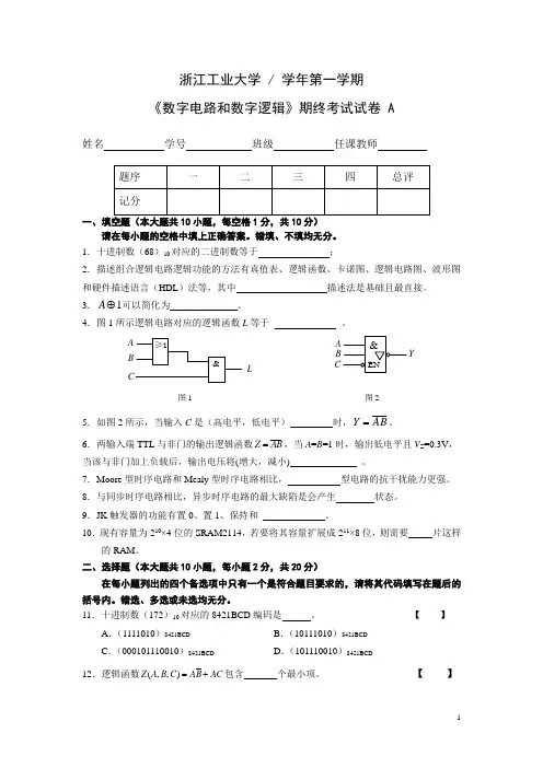
4.图1所示逻辑电路对应的逻辑函数L 等于 。
A B L≥1&CYC图1 图25.如图2所示,当输入C 是(高电平,低电平) 时,AB Y =。
6.两输入端TTL 与非门的输出逻辑函数AB Z =,当A =B =1时,输出低电平且V Z =0.3V ,当该与非门加上负载后,输出电压将(增大,减小) 。
7.Moore 型时序电路和Mealy 型时序电路相比, 型电路的抗干扰能力更强。
8.与同步时序电路相比,异步时序电路的最大缺陷是会产生 状态。
9.JK 触发器的功能有置0、置1、保持和 。
10.现有容量为210×4位的SRAM2114,若要将其容量扩展成211×8位,则需要 片这样的RAM 。
二、选择题(本大题共10小题,每小题2分,共20分)在每小题列出的四个备选项中只有一个是符合题目要求的,请将其代码填写在题后的括号内。
错选、多选或未选均无分。
11.十进制数(172)10对应的8421BCD 编码是 。
【 】A .(1111010)8421BCDB .(10111010)8421BCDC .(000101110010)8421BCD D .(101110010)8421BCD12.逻辑函数AC B A C B A Z +=),,(包含 个最小项。
【 】A .2B .3C .4D .513.设标准TTL 与非门AB Z =的电源电压是+5V ,不带负载时输出高电平电压值等于+3.6V ,输出低电平电压值等于0.3V 。
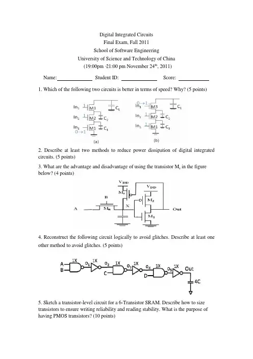
Digital Integrated CircuitsFinal Exam, Fall 2011School of Software EngineeringUniversity of Science and Technology of China(19:00pm–21:00 pm November24th, 2011)Name:Student ID:Score:1. Which of the following two circuits is better in terms of speed? Why?(5 points)2. Describe at least two methods to reduce power dissipation of digital integrated circuits. (5 points)3. What are the advantage and disadvantage of using the transistor M r in the figure below? (4 points)4.Reconstruct the following circuit logically to avoid glitches.Describe at least one other method to avoid glitches. (5 points)5.Sketch a transistor-level circuit for a 6-Transistor SRAM. Describe how to size transistors to ensure writing reliability and reading stability.What is the purpose of having PMOS transistors? (10 points)6.Consider a 24-bit, 6 stage carry-bypass adder with the following delays: t setup=4, t carry=1, t sum=4, t bypass=2.b) Consider the setup delay and carry propagation of the2nd, 3rd, and 4th stages.It is not on the critical path and can be made slower without affecting performance. If each stage is allowed to handle a different number of bits,how many bits would you assign to each of the first four stages to minimize the delay from inputs to the carry outputfor the first16 bits of the adder?(6 points)c)Given the condition that the number of bits in the last two stages is 8, how many bits would you assign to each of the last two stages to minimize the delay of the adder?(4 points)7. Assume the registers in the following figure are edge triggered with t clk-q, max= 4ns, t clk-q, min = 2ns, t setup = 1ns, and t hold= 1ns:CLK(a) What is the maximum operating frequency of this system if there is no skew and jitter? (8 points)(b) What is the maximum random clock skew that this system can tolerate? (6 points)8.Throughout this problem assume that the drain capacitance in the following figure,C D = 0.a) Assuming P(A=0)= P(B=0) = P(C=0) = P(D=0)=0.5, what are the activity factors (i.e.,α0→1) at each of the nodes n0– n3?(6 points)b) Assuming the circuit operates with a supply voltage V DD and a clock frequency f, what is the total dynamic power consumed by this circuit as a function of Cin, C1, C2, and C L (as labeled above)? Note that you should include the power dissipated by driving the A, B, C, and D inputs.(7 points)c)Using the method of logical effort, calculate the delay from A to n2 ((in units of t inv) as a function of Cin, C1, C2, and CL.(5 points)9. Sketch a transistor-level circuit for a master-slave positive edge-triggered register which consists of transmission gates. Express t setup and t hold in terms of t pd_inv(the delay of an inverter) and t pd_tx (the delay of a transmission gate). (7 points)10.What is the logic function performed by this circuit? What is the purpose of having the transistor M1? (4 points)11. Assume that the threshold voltage of NMOS transistors V TN = 0.4V. Calculate the voltage of nodes A and B respectively? (4 points)12.Consider the figure below. During the precharge phase, the output node is precharged to V DD. Assume that all inputs are set to zeros during precharge, and that the capacitance C a is discharged。
………密………封………线………以………内………答………题………无………效……电子科技大学二零一零至二零一一学年第1 学期期中考试模拟电路基础课程考试题卷(120 分钟)考试形式:开卷考试日期20 年11 月7 日课程成绩构成:平时20 分,期中20 分,实验0 分,期末60 分一、填空题(共30分,共 15个空格,每个空格2 分)1.PN结的基本特性是_______________________。
2.PN结的电击穿可以分为___________和__________类型。
3.在放大电路中,测得某三极管三个电极对地的电位分别是:AV=9V,B V =6.7V,C V=6V,该管是 ________ 型的硅管,A端为管子的 ______极,B端为管子的 ___ 极。
4.某晶体管的发射极电流等于1mA,基极电流等于20μA,则它的共射电流放大系数β=________,集电极电流等于_____________。
5. 某放大电路在负载开路时的输出电压为6V,当接入2KΩ负载后,其输出为4V,该电路的输出电阻为____________。
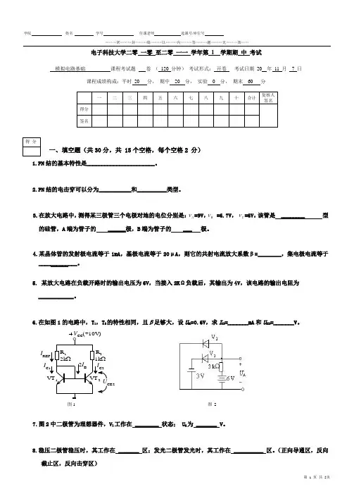
6.在如图1的电路中,T1,T2的特性相同,且β足够大,设U BE=0.6V,求I C2=_______mA和U CE2=_______V。
V(+10V)2ΩIIC2图1 图 27.图2中二极管为理想器件,V1工作在 ________ 状态; U A为 _______ V。
8.稳压二极管稳压时,其工作在 _______ 区;发光二极管发光时,其工作在 __________ 区。
(正向导通区,反向截止区,反向击穿区)………密………封………线………以………内………答………题………无………效……二、 选择题(共15分,每题3 分)1.在图3所示的稳压电路中,稳压管的稳定电压为8V ,稳压管电流小于2mA 时不能稳压。
为使稳压管起稳压作用,则负载电阻R L 应大于( ) A. 4 k Ω B. 1 k Ω C. 800Ω D. 667Ω图 32. 某场效应管的转移特性如图4所示,该管为( )A. N 沟道增强型MOS 管 B. N 沟道耗尽型MOS 管 C. P 沟道增强型MOS 管 D. P 沟道结型场效应管3.三极管工作在放大状态的条件是( )。
安徽大学2010—2011学年第 2学期《 集成电路原理 》(A 卷)考试试题参考答案及评分标准一、简答题(每小题3分,共30分)1. 逻辑综合包括那几步?答:转换(1分)、逻辑优化(1分)和映射(1分)三步。
2. 等比例缩小有几类?答:恒定电场(CE )等比例缩小定律(1分)、恒定电压(CV )等比例缩小定律(1分)和准恒定电场(QCE )等比例缩小定律(1分)。
3. 什么是鸟嘴效应?答:在场区氧化过程中(1分),氧也会通过氮化硅边缘向有源区侵蚀,在有源区边缘形成氧化层,伸进有源区的这部分氧化层被形象地称为鸟嘴(1分),它使实际的有源区面积比版图设计的面积缩小(1分)。
4. 什么是闩锁效应?答:在CMOS 芯片中(1分),在电源VDD 和地线GND 之间由于寄生的PNP 和NPN 双极性BJT 相互影响而产生的一低阻抗通路(1分),它的存在会使VDD 和GND 之间产生大电流,从而破坏芯片或者引起系统错误(1分)。
5. CMOS 反相器的上升时间、下降时间和传输延迟时间的定义是什么?答:上升时间r t 是输出从DD V 1.0上升到DD V 9.0所需要的时间(1分);下降时间f t 是输出从DD V 9.0下降到DD V 1.0所需要的时间(1分);pHL t 表示从输入信号上升边的50%到输出信号下降边的50%所经过的延迟时间,也叫做输出从高向低转换的传输延迟时间,pLH t 表示从输入信号下降边的50%到输出信号上升边的50%所经过的延迟时间,也叫做输出从低向高转换的传输延迟时间(1分)。
6. 版图的检查包括哪些内容?版图的检查包括: 设计规则检查(Design Rule Check ,DRC )(1分); 版图和电路图的一致性检查(Layout Versus Schematic ,LVS )(1分);版图寄生参数提取(Layout Parasitic Extraction ,LPE )和 后仿真。

十四套名校数电考研真题、答案与详解网学天地()出品版权所有!目 录1华中科技大学2008年《电子技术基础》考研真题与答案 (1)2电子科技大学2010年《数字电路》考研真题与答案 (6)3浙江大学2011年《信号系统与数字电路》考研真题与答案 (14)4吉林大学2010年《电子技术》考研真题与答案 (20)5南开大学2011年《电子综合基础》考研真题与答案 (23)6华南理工大学2011年《电子技术基础》考研试题 (27)7哈尔滨工业大学2010年《电子技术基础》考研真题与答案 (33)8哈尔滨工业大学2010年《电路与数字电子技术》考研真题与答案 (39)9哈尔滨工业大学2010年《信号与系统、数字电路》考研真题与答案 (40)10复旦大学2009年《电子线路与集成电路设计》考研真题与答案 (48)11东南大学2008年《信号与系统、数字电路》考研真题与答案 (52)12深圳大学2011年《数字电路与专业综合》考研真题与答案 (60)13重庆大学2010年《电子技术一》考研真题与答案 (67)14北京邮电大学2009年《电子电路》考研真题与答案 (71)网学天地( )出品 版权所有! 11 华中科技大学2008年《电子技术基础》考研真题与答案数字电子技术部分一、填空题(每空1分,共20分)4.数字电路中的三极管一般工作于________区和________区。
答案:截止 饱和5.(63)O 的二进制补码是________,格雷码是________。
答案:(101100)B (101010)B6.四个逻辑变量的最小项最多有________个,任意两个最小项之积为________。
答案:16 07.触发器是对脉冲________敏感的存储单元电路,锁存器是对脉冲________敏感的存储电源电路。
答案:边沿 电平8.对于一个含有逻辑变量A 的逻辑表达式L ,当其他变量用0或1代入后,表达式可化简为:L =________或________时,会产生竞争冒险。
电子科技大学《数字电路》真题2010年(总分140,考试时间90分钟)一、选择题1. 两个二进制数进行算术运算,下面______说法是不正确的。
A.两个无符号数相加,如果最高位产生进位输出,则肯定发生溢出 B.两个最高位不同的补码进行相加运算,肯定不会产生溢出 C.两个补码进行相加运算,如果最高位产生进位输出,则肯定发生溢出 D.两个补码的减法运算可以用加法器来实现2. 以下描述一个逻辑函数的方法中______只能唯一表示。
A.表达式 B.逻辑图 C.真值表 D.波形图3. 在不影响逻辑功能的情况下,CMOS与非门的多余输入端可______。
A.接高电平 B.接低电平 C.悬空 D.通过电阻接地4. 欲产生序列信号11010111,则至少需要______级触发器。
A.2 B.3 C.4 D.55. 一个8位二进制减法计数器,初始状态为00000000,问经过268个输入脉冲后,此计数器的状态为______。
A.11001111 B.11110100 C.11110010 D.111100116. 为构成4096×16的RAM区,共需1024×4位的RAM芯片______片。
A.64 B.8 C.16 D.327. 逻辑函数F1=∑A,B,C,D(2,3,5,8,11,13)和F2=∏A,B,C,D(2,4,7,10,12,13)之间满足______关系。
A.对偶 B.相等 C.香农展开 D.反演8. 移位寄存器由8级触发器组成,用它构成的扭环形计数器具有______种有效状态;用它构成的环形计数器具有______种有效状态,构成线性反馈移位寄存器具有______种有效状态。
A.16,8,511 B.4,8,15 C.16,8,255 D.8,16,1279. 若要将一异或非门当做反相器(非门)使用,则输入端A、B端的连接方式是______。
A.A 或B中有一个接“1” B.A或B中有一个接“0” C.A和B并联使用 D.不能实现10. 实现同一功能的Mealy型同步时序电路比Moore型同步时序电路所需要的______。
2010-2011第二学期B卷参考答案及评分标准安徽大学2010—2011学年第2学期《集成电路原理》(B卷)考试试题参考答案及评分标准一、名词解释题(每小题3分,共15分)1. EDA:Electronic Design Automatic (2分)电子设计自动化(1分)。
2. DRC:Design Rule Check (2分)设计规则检查(1分)。
3.TSPC:True Single Phase Clock (2分)真正的单相时钟(1分)。
4. ASIC:Application Specific Integrated Circuit (2分)专用集成电路(1分)。
5. ULSI:Ultra Large Scale Integrated Circuits (2分)甚大规模集成电路(1分)。
二、编程题(20分)设计一个时钟电路,具有时/分/秒计数功能,完成12小时计数。
答:module counter_h12 (clk, rst, s, m, h);input clk, rst;output [5:0] s, m;output [3:0] h;reg [5:0] s, m; (5 分)always@(posedge clk or posedge rst)if(rst)s<=6’b000000;else if (s= =6’b111011)s<=6’b000000;elses<=s+1; (5 分)always@( posedge clk or posedge rst)if (rst)m<=6’b000000;else if (s= =6’b111011)beginif(m= =6’b111011)m<=6’b000000;elsem<=m+1;end (5 分)always@( posedge clk or posedge rst)if(rst)h<=4’b0000;else if ((s= =6’b111011)&&(m= = 6’b111011))beginif(h= =4’b1011)h<=4’b0000;elseh<=h+1;endendmodule (5 分)三、简答题(每小题4分,共20分)1.集成电路的设计方法分为哪三种?答:基于PLD的设计方法(2分),半定制设计方法(1分),定制设计方法(1分)。

目 录第一部分 中国科学技术大学808电路与电子线路考研真题2014年中国科学技术大学电路与电子线路考研真题2013年中国科学技术大学电路与电子线路考研真题2012年中国科学技术大学电路与电子线路考研真题第二部分 兄弟院校电路与电子线路考研真题2015年电子科技大学815电路分析基础考研真题2014年重庆大学840电路原理一考研真题2012年厦门大学846电子线路(含模拟和数字)考研真题2012年华东师范大学883电子线路(含模拟、数字)考研真题第一部分中国科学技术大学808电路与电子线路考研真题2014年中国科学技术大学电路与电子线路考研真题2014年硕士学位研究生入学考试试题(鬼路与电子线路)所有试题答案写在答题舐上,答案写在试卷上无效s需使用计算器□不使用计算器一、填空(每题4分,共16分)1.对任一含“个节点、力条支路的电蹬,可以列出的独立KCL方程数为应,独立KVL方程数为鱼。
2.电路如图1-1折示,剧等效电感L舛=全图1-1图)-2图1-33.电路如S1-2.〃为纯电阻网络,E)开关闭台前电路为稳态.已知虬〔TV,虬疽/'V"之。
*),电路全响应为%(。
=(2+5广+3产)丫(佗0+)「则峋的零输入响应为®,4.用路如图1-3,N为线性含源电阻网络,《=1V时,虬=2V;孔=2V盹,%=3V,则七=3V时,岭=曳>二、计算(共34分)1.(12分)电路如图2-L按图中标注.(1)列出三个回路电流方程|(2)以节点0为参考节瘤,列出三个节点电压方程,(无需求解)图E 考试科目;电肆与珥子城路第I页共4页2.(10分)如图2・2,电路原处于稳态,E时开关S打开,求X的/(r)。
一1+$13.(12分)电路如图2-3,二端口网络N的运算阻抗参数矩阵Z(s)=Q o11+r(1)求网络函数=:(2)若上=2。
顷珀)A,求零状态响应u2(0,如)三、简答或简算(每题5分,共20分)1.室温下,实际二极管加正向偏置电压,流过二极管的宜流电流为2mA,求此时二极管的交流电阻值。

电子科技大学二零零九至二零一零学年第 二 学期期 末 考试数字逻辑设计及应用 课程考试题 A 卷(120分钟)考试形式:闭卷 考试日期2010年7月12日课程成绩构成:平时 20 分, 期中 20 分, 实验 0 分, 期末 60 分一、To fill your answers in the blanks (1’×25)1. If [X]10= - 110, then [X]two's-complement =[ 10010010 ]2,[X]one's-complement =[ 10010001 ]2. (Assumed the number system is 8-bit long) 2. Performing the following number system conversions: A. [10101100]2=[ 000111010010 ]2421B. [1625]10=[]excess-3C. [ 1010011 ]GRAY =[10011000 ]8421BCD3. If ∑=C B A F ,,)6,3,2,1(, then F D ∑=C B A ,,( 1,4,5,6 )=C B A ,,∏(0,2,3,7 ).4. If the parameters of 74LS-series are defined as follows: V OL max = 0.5 V , V OH min = 2.7 V , V IL max = 0.8 V , V IH min = 2.0 V , then the low-state DC noise margin is ,the high-state DC noise margin is .5. Assigning 0 to Low and 1 to High is called positive logic. A CMOS XOR gate in positive logic is called XNOR gate in negative logic.6. A sequential circuit whose output depends on the state alone is called a Moore machine.7. To design a "001010" serial sequence generator by shift registers, the shift register should need 4 bit as least.8. If we use the simplest state assignment method for 130 sates, then we need at least 8 state variables.9. One state transition equation is Q*=JQ'+K'Q. If we use D flip-flop to complete the equation, theD input terminal of D flip-flop should be have the function D= JQ'+K'Q.10.Which state in Fig. 1 is ambiguous D11.A CMOS circuit is shown as Fig. 2, its logic function z= A’B’+ABFig. 1 Fig. 212.If number [A]two's-complement =01101010 and [B]one's-complement =1001, calculate [A-B]two's-complement and indicate whether or not overflow occurs.(Assumed the number system is 8-bit long)[A-B]two's-complement = 01110000, overflow no13. If a RAM’s capacity is 16K words × 8 bits, the address inputs should be 14bits; We need 8chips of 8K ⨯8 bits RAM to form a 16 K ⨯ 32 bits ROM..14. Which is the XOR gate of the following circuit A .15.There are 2n-n invalid states in an n-bit ring counter state diagram.16.An unused CMOS NOR input should be tied to logic Low level or 0 .17.The function of a DAC is translating the Digital inputs to the same value of analogoutputs.二、Complete the following truth table of taking a vote by A,B,C, when more than two of A,B,C approve a resolution, the resolution is passed; at the same time, the resolution can’t go through if A don’t agree.For A,B,C, assume 1 is indicated approval, 0 is indicated opposition. For the F,A B C F0 0 0 0三、The circuit to the below realizes a combinational function F of four variables. Fill in the Karnaugh map of the logic function F realized by the multiplexer-based circuit. (6’)四、(A) Minimize the logic function expressionF = A·B + AC’ +B’·C+BC’+B’D+BD’+ADE(H+G) (5’)F = A·B + AC’ +B’·C+BC’+B’D+BD’= A·(B ’C )’ +B’·C+BC’+B’D+BD’= A +B’·C+BC’+B’D+BD’+C ’D (或= A +B’·C+BC’+B’D+BD’+CD ’)= A +B’·C+BD’+C ’D (或= A + BC’+B’D +CD ’)(B) To find the minimum sum of product for F and use NAND-NAND gates to realize it (6’)=),,,(Z Y X W F Π(1,3,4,6,9,11,12,14)------3分 F= X ’Z ’+XZ -----2分 =( X ’Z ’+XZ)’’=(( X ’Z ’)’(XZ)’)’ ------1分五、Realize the logic function using one chip of 74LS139 and two NAND gates.(8’)∑=)6,2(),,(C B A F ∑=)3,2,0(),,(E D C GF(A,B,C)=C’∑(1,3) ---- 3分 G(C,D,E)=C’∑(0,2,3) ----3分六、Design a self-correcting modulo-6 counter with D flip-flops. Write out the excitation equations and output equation. Q2Q1Q0 denote the present states, Q2*Q1*Q0* denote the next states, Z denote the output. The state transition/output table is as following.(10’)Q2Q1Q0Q2*Q1*Q0*Z000 100 0100 110 0110 111 0111 011 0011 001 0001 000 1激励方程式:D2=Q0’D1=Q2D0=Q1修改自启动:D2=Q0 +Q2Q1’D1=Q2+Q1Q0’D0=Q1+Q2Q0输出方程式:Z=Q1’Q0得分七、Construct a minimal state/output table for a moore sequential machine, that will detect the input sequences: x=101. If x=101 is detected, then Z=1.The input sequences DO NOT overlap one another. The states are denoted with S0~S3.(10’)For example:X:0 1 0 1 0 0 1 0 1 0 1 1 0 1 1 0 0 0 1 1 ……Z:0 0 0 1 0 0 0 0 1 0 0 0 0 1 0 0 0 0 0 0 ……state/output tableS X Z 0 1 S0 S0 S1 0 S1 S2 S1 0 S2 S0 S3 0 S3 S0S11 S*八、Please write out the state/output table and the transition/output table and the excitation/output table of this state machine.(states Q2 Q1=00~11, use the state name A~D )(10’)Transition/output table State/output table Excitation/output tableQ2Q1 X Z 01 00 01 11 1 01 00 10 1 10 01 01 0 11 01 01 1Q2*Q1*SX Z 0 1 A B D 1 B A C 1 CB B 0 DBB1S*Q2Q1 X Z 01 00 01 11 1 01 00 10 1 10 01 01 0 11 01 01 1D2 D1得 分九、Clocked Synchronous State Machine Design(15’)74x163 is a synchronous 4-bit binary counter with synchronous CLEAR input and LOAD input. LD_L=(Q B Q C)', CLR_L=(Q D'Q B)'in the following circuit.1. Finish the logic circuit.2. Draw the state diagram with all states of “Q3Q2Q1Q0” . (“Q3Q2Q1Q0” is the output of 74x163)3. Write the sequence of Y.Y is the output of 74x151. (Assumed state of 74x163 start in Q3Q2Q1Q0=0000.)YCLOCK====Word 行业资料分享--可编辑版本--双击可删====解答:(1) Finish the logic circuit.(见下页图) LD_L=(Q B Q C )', CLR_L=(Q D 'Q B )' (2) Q3Q2Q1Q0: 清零优先级高于置数 0000—0001—0010—0000 0011—00000100—0101—0110—0000 0111—00001000—1001—1010—1011--1100—1101—1110--11001111—1100 (3) Y=010*******Function table for a 74x163Inputs Current State Next state OutputCLR_L LD_L ENT ENP Q D Q C Q B Q A Q D * Q C * Q B * Q A * RCO 0 X X X X X X X 0 0 0 0 0 1 0 X X X X X X D C B A 0 1 1 0 X X X X X Q D Q C Q B Q A 0 1 1 X 0 X X X X Q D Q C Q B Q A 0 1 1 1 1 0 0 0 0 0 0 0 1 0 1 1 1 1 0 0 0 1 0 0 1 0 0 1 1 1 1 0 0 1 0 0 0 1 1 0 1 1 1 1 0 0 1 1 0 1 0 0 0 1 1 1 1 …………. ………….. 0 1 1 1 1 1 1 1 1 0 0 0 0 1====Word行业资料分享--可编辑版本--双击可删====。
数电期中测试题 参考答案系别 班级 学号 姓名一、单项选择题(本大题共7小题,每小题2分,共14分)在每小题列出的四个备选项中只有一个是符合题目要求的,请将其代码填写在题后的括号内。
错选、多选或未选均无分。
1.十进制数25用8421BCD 码表示为(B )A.10101B.0010 0101C.100101D.110012.函数B A ABC ABC F //++=的最简与或式是(D )A.F=A+BB.//C A F +=C.F=B+CD.F=B3.若将一个同或门(输入端为A,B )当作反相器使用,则A 、B 端应(C )A.A 或B 中有一个接1;B.A 和B 并联使用;C. A 或B 中有一个接0;D.同或门无法转换为反相器4.符合下面真值表的门电路是(C )A.与门B.或门C.同或门D.异或门5.下列代码属于8421BCD码的是(C)A.1010B.1100C.0111D.11016.最小项''A BC D的逻辑相邻最小项是(B)A.''ABCD D.'AB CDA BC D C.'A B CD B.'''7.函数F=AB+BC,使F=1的输入ABC组合为(D)A.ABC=000 B.ABC=010C.ABC=101 D.ABC=110二、填空题(本大题共10小题,每小题2分,共20分)请在每小题的空格中填上正确答案。
错填、不填均无分。
1.基本逻辑运算有_______、、3种。
与、或、非2.描述逻辑函数各个变量取值组合和函数值对应关系的表格叫_真值表。
3.函数Y=AB+AC 的最小项之和表达式为________。
(ABC ABC C AB Y ++=//) 4.3线-8线译码器74LS138处于译码状态时,当输入A 2A 1A 0=001时,输出/0/7~Y Y =______。
111111015.能够将1个输入数据,根据需要传送到m 个输出端的任何一个输出端的电路叫_______。
华中科技大学2010年招收硕士研究生入学考试试题答案 科目代码及名称: 电路理论 814 适用专业: 电气工程所有专业、环境工程一、答案解析:本题是基本题型,首先可想到节点电压方程,但由于本题有一个电流源未知,也可采用叠加法,下面用两种方法讨论。
答案详解:法一:节点电压法,节点标注如下 +-+-23V 5V 5A Ω3Ω4Ω1Ω2S I 012341.电阻电流方向为1-012433241U -U 23U -U 5U U U 10412U 133=⎧⎪=⎪⎪⎨+++=⎪⎪=⨯=⎪⎩解之得 1234U 3U -20U 1U 6====对节点4运用基尔霍夫电流定理s 61-5021I ++= 解之得 s 1I =发出功率 355-10W 1P =⨯=()2:电阻电流方向为0-112433241U -U 23U -U 5U U U -10412U -13-3=⎧⎪=⎪⎪⎨++=⎪⎪=⨯=⎪⎩ 解之得 12341025U -3U -26U U 33====对节点4运用基尔霍夫电流定理05-1310I 2325s =++5.2-I s =发出功率 W 3251310-55P =⨯=)(法二:叠加法1:电阻电流方向为1-0当电流源置0电压源单独作用时电路如下 +-+-23V 5VΩ3Ω4Ω1Ω2I237I '=当电压源置0电流源单独作用时电路如下5AΩ3Ω4Ω1Ω2S I I ''s 44I -577I ''=⨯ s 2344I -51777I I I '''=+=+⨯= 1A S I =另一种情况类似,略。
二、答案解析:理想运放问题,节点电压法,列方程可求出。
答案详解: +-+∞+-+∞+-+-1o u 2o u i u 1R 2R 3R 4R 5R +-o u 12313233o14511212232o212243U 0U 0U -U U -U R R U U U -U R R U -U U -U U -U R R R i =⎧⎪=⎪⎪=⎪⎪⎨-⎪=⎪⎪⎪=+⎪⎩ 25o114232o21114R R U U R R R R R R3U -U (R R R R i i ⎧=⎪⎪⎨⎪=++⎪⎩) 23252o o1o2111414R R R R R R3U U U U ()R R R R R R i =-=+++三、答案解析:本题是正弦稳态问题,可考虑直接用电流回路法,但复数三阶方程很难解,所以可考虑,1只设出两个电感线圈上的电流,再求出其他支路电流列方程求解,2由叠加法,逐个电源求解,看是否能解耦线圈。
5.1分布参数电路与集总参数电路的区别是什么?答:分布参数电路和集总参数电路的区别是:分布参数电路频率高,波长短可以和电路尺寸想比较,同时电参量随空间变化,电磁波在电路中传输效应很明显,传输线上的电感,电阻和线间的电导都不能忽略,线上各点电位不同,处处有储能和损耗,集总参数电路的频率则比较低,电路尺寸和波长相比较很小,可以认为是一点,电场和磁场可以近似看做只随时间变化,不随导线长度、位置而发生变化。
5.2传输线有哪些特性参量和工作参量?他们是如何定义的? 答:传输线的特性参量包括特性阻抗,传播常数,相速和波导波长 特性阻抗:传输线上行波电压与电流之比 传播常数))((1111jwC G jwL R ++=λ 相速:行波等波阵面等相位面移动的速度 波导波长:波在一周期内沿线所传播的距离传输线的工作参量包括输入阻抗,反射系数,驻波系数,驻波相位。
输入阻抗:线上任意一点(参考点)的总电压与总电流的比值称为由该点向负载看去的输入阻抗。
反射系数:是传输线上某点反向传播的波(反射波)电压与正向传播的波(入射波)的电压之比称为该点的反射系数。
驻波系数:驻波系数是传输线上电压最大值和电压最小值的比值。
驻波相位(电压驻波比):从负载处沿波源方向到离负载最近的电压最小值处的距离。
5.3 设一段长为L 的有耗传输线,当负载开路()0=I L 时,测得输入端阻抗为z 0,当负载端短路)0(=U l 时,测得输入端阻抗为z s ,计算该线的特性阻抗z c 。
解: z th z th ZZ Z Z Z Z lcc lcinγγ++= 当0=Z l (短路) 当∞=Z l (开路) 解之得到5.4 一段终端短路的传输线,线长l=2cm ,工作频率H fz G 31=,H fz G 62=。
试判断输入阻抗分别呈何特性。
若传输线的特性阻抗z c =50Ω,Ω=262)(j l Z ,试求上述两频率下短路线的长度。
解:当H fz G 3=时π52tg j z z c in = 感性的当H fz G 6=时π54tg j z z c in = 容性的当Ω=256j z in 时 对于H f z G 3=解得 cm l 2.2= 对于H fz G 6=解得 cm l 1.1=5.5以知无耗传输线的负载阻抗Ω+=2525j z l ,特性阻抗Ω=50z c ,求传输线上的反射系数,驻波系数和距离终端4/λ处的输入阻抗。
《数字电路》期中考试试卷一、填空题(每空1分,共20分)1、(、101)2=10=8421BCD2、一个 JK 触发器有个稳态,它可存储位二进制数。
3、三态门的输出状态有、、三种状态。
4、对160个符号进行二进制编码,则至少需要位二进制数。
5、A=(-59)10,A的原码是,补码是。
6、使用与非门时多余的输入端应接电平,或非门多余的输入端应接电平。
7、触发器有个稳态,存储8位二进制信息要个触发器。
8、3线—8线译码器有条输入线,条输出线。
9、组合逻辑电路的冒险有型冒险和型冒险。
10、对于JK触发器的两个输入端,当输入信号相反时构成触发器,当输入信号相同时构成触发器。
二、选择题(每题2分,共20分)1.和逻辑式相等的式子是( )A.AC+B B. BC C.B D.2.32位输入的二进制编码器,其输出端有( )位。
A、256B、128C、4D、53.4个边沿JK触发器,可以存储( )位二进制数A.4B.8C.164.三极管作为开关时工作区域是( )A.饱和区+放大区B.击穿区+截止区 C.放大区+击穿区D.饱和区+截止区5、在四变量卡诺图中,逻辑上不相邻的一组最小项为:() A.m1 与m3 B.m4 与m6 C.m5 与m13D.m2 与m86.L=AB+C 的对偶式为:()A 、 A+BCB 、 (A+B)C C 、 A+B+CD、 ABC7.逻辑函数F(A,B,C)= AB+B C+AC的最小项标准式为()。
A.F(A,B,C)=∑m(0,2,4)B.F(A,B,C)=∑m(1,5,6,7)C.F(A,B,C)=∑m (0,2,3,4)D.F(A,B,C)=∑m(3,4,6,7)8.逻辑电路如图1所示,其逻辑功能相当于一个()。
A.“与”非门B.“导或”门C.“与或非”门图19.三输入、八输出译码器,对任一组输入值其有效输出个数为()。
A.3个B.8个 C.1个D.11个10、逻辑函数F==( )。
温州大学期中考试试卷 2009-2010学年第 2 学期注:8+10+8+8+10+5+8+8+10+10+7+8=1001.(本题8分)将下列十进制数转换为二进制数,八进制数和十六进制数(要求转换误差不大于 2-4): (1)(127)D =(2)(2.718)D =2. (本题10分)逻辑函数化简 (1) 用代数法化简(2) 用卡诺图法化简学院-------------------------------------- 班级---------------------------------- 姓名------------------------------------- 学号-------------------------------------3. (本题8分)设有一个74LS04反相器驱动两个74ALS04反相器和四个74LS04反相器。
(1)问驱动门是否超载?(2)若超载,试提出一改进方案;若未超载,问还可增加几个74LS04门?(74LS04参数为:I OL(max)=8mA, I OH(max)=0.4mA;I IH(max)=0.02mA;VOL(max)=0.5V )4. (本题8分)设计一发光二极管(LED)驱动电路,设LED的参数为V F=2.5V,I D=4.5mA; 若V cc=5V,当LED发亮时,电路的输出为低电平,选出集成门电路的型号,并画出电路图.5. (本题10分)某足球评委会由一位教练和三位球迷组成,对裁判员的判罚进行表决。
当满足以下条件时表示同意:有三人或三人以上同意;或者有两人同意,但其中一人是叫教练。
试用2输入与非门设计该表决电路6. (本题5分)判断图所示电路在什么条件下产生竞争冒险,怎样修改电路能消除竞争冒险?7. (本题8分)用译码器74HC138和适当的逻辑门实现函数8. (本题8分)应用74HC151实现逻辑函数L=(A⊙B)⊙C9. (本题10分)由4位数加法器74HC283构成的逻辑电路如图所示,M和N为控制端,试分析该电路的功能。
中国科学技术大学苏州研究院软件学院
数字集成电路设计
期中考试
(2010年10月11日2:00pm—3:30pm)
1.问答题
a)叙述摩尔定律(5分)。
b)叙述评价数字集成电路设计质量的四个基本特性(6分)。
c)叙述长沟MOS晶体管与短沟MOS晶体管的区别(6分)。
d)MOS管的电容由哪几部分构成?并说出在不同工作模式下的区别(8分)。
e)以反相器为例,说出静态CMOS电路的功耗包括哪几部分(6分)?
f)数字集成电路按比例缩小有几种情形(6分)?
g)下面的两种电路哪个性能(速度)更优越一些?并说出原因(5分)。
h)下面的电路哪个是无比逻辑,哪个是有比逻辑?并说出有比逻辑与无比
逻辑的区别(5分)。
2.下图为一RC网络。
计算:
a)从输入In到Out1的Elmore延时(5分);b)从输入In到Out2的Elmore延时(5分);c)确定哪条路径是关键路径(3分)?
3.假设下图中反相器由标准CMOS实现,并且具有对称的电压传输特性。
假设
C intrinsic = C gate (γ=1),单位尺寸反相器的等效电阻与电容为R和C。
单位尺
寸反相器的本征延时为t inv。
反相器inv2, inv3和inv4的尺寸S1,S2和S3不小于1。
a)确定S1,S2和S3使时延最小(5分),并计算总的最小时延(以t inv为单位)
(5分)。
b)确定反相器inv2, inv3和inv4的尺寸S1,S2和S3使功耗达到最小(4分)。
4.如下图所示的逻辑网络,要求确定复合门电容y和z使A端到B端延时最小。
a)计算A端到B端总的逻辑努力LE(3分);b)计算A端到B端总的电气努力F (2分);c)计算A端到B端总的分支努力B (3分);d)计算A端到B端总的路径努力PE (2分);e)确定最佳级努力SE (3分)(近似为整数);f)确定A端到B端的最小时延(以t inv为单位)(3分);g)确定电容y (5分);h)确定电容z (5分)。