高云半导体开始提供GW2A—55K的FPGA工程样片
- 格式:doc
- 大小:11.00 KB
- 文档页数:1

AGM 国产高端FPGA 系列产品线发布,国产FPGA芯片市场再进一步遨格芯AGM FPGA(以下简称AGM )今天宣布AGM 国产高端FPGA 系列产品线BlueWind 正式发布,并将在2017 年第二季度开始供货。
BlueWind 软件芯片结构和产品系列,适用于如通讯,安防视频,数据中心加速,和AI 所需高速运算。
AGM 推出的BlueWind 系列的FPGA 产品瞄准的是高性能高容量的高存量市场,和运算加速市场。
AGM FPGA 凭借自身积累的对标美国硅谷FPGA 公司的高容积率(99+%)产生的高容量技术,研发集成逻辑单元容量从10万至100 万门不等,其产品与主流厂商产品Xilinx Virtex,做到管脚和高性能兼容,提供从55nm,40nm,28nm 的产品系列。
AGM 拥有自主知识产权的电路结构和基于自有电路的编译软件,在芯片内部接口兼容主流厂商器件,PCB 板级可以直接替换并用AGM 编译软件导入烧写,可大大降低客户的替换成本。
AGM 在杭州、上海和北京设有办公室,自公司2012 年创办以来,始终专注于研发自主知识产权的FPGA 核心软件和硬件技术。
已经推出三个系列的CPLD、FPGA、Programmable SoC 产品进入量产,已得到多家知名厂商认证,在多元化的市场量产出货,是首家得到国内商用市场认可的国产FPGA供应商,并通过三星供应商认证的产品。
其FPGA 产品系列基于对LED 多彩市场对高容积率(90+%)、低成本、高品质的市场需求入手,AGM 已切入并在华东市场产生垄断性市场占入率,并以此推向其他多元化市场。
其CPLD 产品线基于客户对产品的软件兼容性要求极高的市场要求,研发出兼容软件系统方便客户,目前也已是国产CPLD 市占率遥遥领先。
AGM 1K 容量产品器件,以其超低的市场售价和超低的运算功耗在逐步打入消费类市场,提供线上销售和设计支持的商业模式服务于高量出货客户。

高云半导体涉足国产FPGA新领域—车载芯片广东高云半导体科技股份有限公司(以下简称“高云半导体”)宣布将向客户提供支持汽车级温度范围的FPGA 器件。
此前,高云半导体已经推出了两个家族的FPGA 系列产品,分别是使用嵌入式闪存工艺的非易失FPGA 小蜜蜂®家族和基于SRAM 的中密度FPGA 晨熙®家族,这两个家族的器件均已支持商业级(0C°-85C°)和工业级(-40C°~+100C°)温度标准。
此次推出支持汽车级温度范围(-40C°~+125C°)的为小蜜蜂®家族部分FPGA 器件。
高云半导体小蜜蜂®家族的FPGA 器件具有低功耗、高性能、多用户I/O、用户逻辑资源丰富,支持高速LVDS 接口,支持可随机访问的用户闪存模块等特点;且在芯片系统上电启动方面,为用户提供了丰富的选择:Auto boot、片内或片外Flash 先启动的Dual boot,以及片外Flash 多分区的Multi-boot 功能等方式。
在接口方面,小蜜蜂®家族的FPGA 器件率先支持全球最新标准I3C 以及可用GPIO 实现的MIPI D-PHY 标准。
I3C 标准支持Push-Pull SDR、HDR-DDR 标准,其最高数据速率可达12.5Mbps,并可双向传输,且兼容早期的I2C。
GPIO 内置MIPI HS/LP 模式切换处理电路,不需要再外加匹配电阻,大大简化了用户的系统设计和PCB 设计。
“高云半导体已就汽车级芯片的AEC-Q100 标准以及零失效(Zero Defect)的供应链品质管理标准ISO/TS 16949 等规范展开了资质认证工作。
鉴于我们供应商的相关生产线已取得此类认证,预期我们的认证工作会相对顺利一些”,高云半导体运营总监吴兆淋先生表示。
“汽车电子市场是半导体企业极为关注的一个新兴增长点。


高云半导体推出通用LVDS变速箱接口解决方案广东高云半导体科技股份有限公司(以下简称“高云半导体”)今天宣布推出同时支持非易失小蜜蜂®家族GW1N 系列以及中密度晨熙®家族GW2A 系列FPGA 芯片的通用LVDS 变速箱接口IP 核(Gowin Generic LVDS Gearbox IP),包括相关软核、参考设计及开发板等完整解决方案。
下面就随半导体小编一起来了解一下相关内容吧。
高云通用LVDS 变速箱接口IP 实现了内部逻辑和外部接口之间时钟频率和数据位宽的切换,并保证数据吞吐量守恒,同时支持发送功能和接收功能,高云所有FPGA 芯片收发变速箱切换比例都支持1:1、1:2、1:4、1:7、1:8 和1:10。
此外GW1N-6/9 器件还支持1:16 切换比例。
针对随路时钟和随路数据相位关系的不同需求,高云通用LVDS 变速箱接口解决同时支持边沿对齐方式和中间对齐方式。
高云FPGA 芯片提供专用的单元模块用于构建高速LVDS 接口,可根据客户特定的带宽、对齐方式、收发功能以及切换比例需求,整合单元模块并协同工作实现相应的功能。
l 高速低偏斜时钟HCLK 用于支持I/O 完成高性能数据传输;l GCLK 是内部系统时钟,内部系统时钟必须使用全局时钟网络;l 高速时钟分频模块,生成和输入时钟HCLK 相位一致的分频时钟GCLK;l 锁相环模块实现时钟的倍频、分频和相移;l 串行转并行接收侧模块实现变速箱功能;l 并行转串行发送侧模块实现变速箱功能;l 每个I/O 都包含延迟模块,总共提供的延迟大约为128 步x25ps=3200ps。
“高云通用LVDS 变速箱接口IP 充分利用了高云FPGA 芯片内嵌的各种专用。
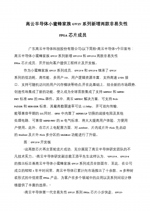
高云半导体小蜜蜂家族GW1N系列新增两款非易失性FPGA芯片成员广东高云半导体科技股份有限公司(以下简称“高云半导体”)今日宣布:高云半导体小蜜蜂家族GW1N系列新增GW1N-9和GW1N-6两款非易失性FPGA芯片成员,并开始向客户提供工程样片及开发板。
作为小蜜蜂家族GW1N系列成员,GW1N-9和GW1N-6继承了GW1N系列的低功耗、高性能、多用户I/O、用户逻辑资源丰富,支持高速LVDS接口,支持可随机访问的用户闪存模块等特点;并在此基础上,结合新的市场趋势,创造性地集成了新的功能,使之成为全球首款集成了支持MIPII3C和MIPID- PHY标准GPIO的FPGA器件。
其中,高云MIPII3C解决方案,可支持Push- PullSDR和HDR-DDR标准,其最高数据速率可达12.5Mbps,并可双向传输,能够兼容早期的I2C;同时,GPIO中内置了MIPIHS/LP切换的端接电阻及其他处理电路,可兼容MIPID-PHY的IO电气标准,将大大提高用户体验,方便用户使用。
此外,在芯片上电配置方面,对Autoboot、片内或片外Flash先启动的Dualboot及片外Flash多分区的MultiBoot功能进行了升级。
图:GW1N-9开发板“这两款芯片再次首轮流片成功,充分展现了高云半导体研发团队的不凡技术实力。
”高云半导体研发副总裁王添平先生这样认为,“GW1N-9、GW1N-6 的推出标志着高云半导体小蜜蜂家族GW1N系列成员全部面市,至此,在公司成立的短短3年半时间里,高云半导体已累计向市场推出了十余款、50多种封装形式的中低密度FPGA产品,为客户在多个领域中的应用以及系列间设计移植提供了丰富的选择。
”“高云半导体第一代非易失性GW1N系列FPGA芯片小步快走,GW1N-6和GW1N-9在继承了GW1N-1/2/4的众多优点的基础上,加入了多项创新的特性,使得高云半导体在非易失性FPGA领域逐步建立了领先优势。
GW2A/GW2AR系列FPGA产品原理图指导手册简介使用高云半导体GW2A/GW2AR系列FPGA产品做电路板设计时需遵循一系列规则。
本文档详细描述了GW2A/GW2AR系列FPGA产品相关的一些器件特性和特殊用法,并给出校对表用于指导原理图设计,主要内容如下:●电源●JTAG下载●MSPI下载●时钟管脚●差分管脚●READY、RECONFIG_N、DONE●MODE●JTAGSEL_N●FASTRD_N●EXTR●配置管脚复用●外接晶振电路参考●GW2AR Bank电压●各器件支持的配置模式●管脚分配电源1.概述GW2A/GW2AR系列FPGA产品电压种类包括V CC核电压、V CCPLL锁相环电压、V CCX辅助电压和V CCIO Bank电压。
V CCX为辅助电源,用于给芯片内部部分电路供电,需要接2.5V或者3.3V 电压,如果V CCX电压不接,会影响IO、OSC、BSRAM等电路工作,造成芯片无法使用。
2.电源指标建议在推荐的工作条件及工作范围内使用高云器件,超出工作条件及工作范围的数据仅供参考,高云半导体不保证所有器件都能在超出工作条件及工作范围的情况下正常工作。
表1列出了各电源电压的推荐工作范围。
3.总体功耗针对特定密度、封装和资源利用率,可以使用云源软件内嵌的GPA工具进行功耗评估和分析。
4.上电时间电源上电时间参考范围值:0.2ms ~2ms。
注!●如果上电时间>2ms,则需要确保上电顺序为先V CC,后V CCX/V CCIO;●如果上电时间<0.2ms,建议增加电容以延长上电时间。
5.电源滤波每一个FPGA电源输入脚就近连接一个0.1uF陶瓷电容到地;对于VCC核电压输入端要重点进行噪声处理,具体参考如图1所示:图 1 VCC核电压输入端噪声处理V1P0VCCFBC4.7uFGW2A/GW2AR系列FPGA产品需要对V CCPLL隔离滤波,具体参考如图2所示:图2隔离滤波V CCPLLV1P0VCCPLLFBC4.7uF C C 100nF10nF其中FB为磁珠,参考型号MH2029-221Y,4.7uF、100nF、10nF均为陶瓷电容,精度不低于±10%。
的设计师选择用FPGA,因为可以很快地实现创新。
高云的FPGA是一个平台,软件工具略对芯片安全、国产化需求提升,国际巨头激烈竞争、产业调整给自主FPGA带来机会和人才溢出,国内FPGA厂商竞争也带来DK-DEV-GW2A55的软硬件目前已申请国内专利22项,其中发明专利12项,3项已进入实质审查阶段,授权使用新型专利2项,已申请国外发明专利2项,登记软件著作权8项。
民营企业的体会与建议对一家投身于半导体技术领域的民营企业而言,常常面临着资金、人才、技术等方面的壁垒,对此,高云亦深有体会,对政策、人才也极为渴求。
对民营企业来说,首先政策指引十分重要。
高云进入FPGA领域的缘起,也是因为高云董事长陈天成在国家政策的号召之下毅然决然地进入这个领域。
由于FPGA领域非常专业,如何让投资人理解并投入到这个领域的开发中来确实不是一件易事。
正是政策的号召力,令陈天成力排众议,决定做这个项目希望切实为国家做一些事情。
其次,要有一支优秀的国际队伍。
人才是公司创新生命力的保证。
高云聚集了一批优秀的国际人才。
为了吸引到人才,高云建立了持续的内外人才引进制度和持续创新机制,为人才的才能发挥建立良好的环境。
通过股权等方式推动高云的持续创新,提升产品竞争力。
对于高科技企业来讲,人才一直都是最宝贵的财富。
没有人才,没有新产品的持续推出,这个高科技企业的价值也就消失殆尽。
最后,要建立切实可行的自主FPGA研发中长期目标,夯实基础。
FPGA产业需要引导各类国家基金进入,将自主FPGA做大做强。
建立切实可行的FPGA芯片产业联盟,产学研协同开发,实现一揽子突破,带动国内学术深入及人才培养;组织产业链上下游从FPGA芯片设计、制造、封装、测试到系统应用协同开发,实现一条龙计划。
大力支持企业中低密度FPGA产品做实打好软硬件基础,推动全面产业化。
做好上述几点,中国FPGA企业将会获得更广泛的生机。
责任编辑:孙俊杰sunjunjie@DK-ENTRY-GW1N1。
GW2A/GW2AR series of FPGA ProductsSchematic ManualIntroductionUsers should follow a series of rules during circuit board design when using the GW2A/GW2AR series of FPGA products. This manual describesthe characteristics and special features of GW2A/GW2AR series FPGAproducts and provides a comprehensive checklist to guide designprocesses. The main contents of this guide are as follows:●Power Supply●JTAG download●MSPI download●Clock pin●Difference pin●READY, RECONFIG_N, DONE●MODE●JTAGSEL_N●FASTRD_N●EXTR●Pin Multiplexing●Reference for the external crystal oscillator circuit●GW2AR Bank voltage●Supported configuration modes●Pin DistributionPower Supply1. OverviewVoltage types of the GW2A/GW2AR series of FPGA products include core voltage (V CC), PLL voltage (V CCPLL), auxiliary voltage (V CCX) and Bankvoltage (V CCIO).V CCX is an auxiliary power supply that is used to connect the internal part of the chip, with a 2.5V or 3.3V power supply. If no V CCX exists, I/O,OSC, and BSRAM circuits will be impacted and the chip will not befunctional.2. Power IndexUsers should ensure GOWINSEMI products are always used withinrecommended operating conditions and range. Data beyond the working conditions and range are for reference only. GOWINSEMI does notguarantee that all devices will operate as expected beyond the standard operating conditions and range.Table 1 lists the recommended working range for each power voltage.3. Total PowerFor specific density, packages, and resource utilization, GPA tools can be used to evaluate and analyze the power consumption.4. Power-on timeReference range of power-on time: 0.2 ms ~ 2 ms.Note!● If the power-on time is more than 2ms, you need to ensure that the power-on in sequence is V CC , and then V CCX /V CCIO ;●If the power-on time is less than 0.2ms, it is recommended to increase the capacitance to prolong the power-on time.5. Power FilterEach FPGA power input pin is connected to the ground with a 0.1uF ceramic capacitor.The input end of the V CC core voltage should primarily conduct the noise processing. Specific reference is as shown in Figure 1:Figure 1 Noise Processing of the Input End of the V CC Core VoltageGW2A/GW2AR series of FPGA products isolate and filter the V CCPLL . Specific reference is as shown in Figure 2:Figure 2 Isolate and Filter the V CCPLLFB is a magnetic bead, reference model mh2029-221Y , ceramic capacitance 4.7uF, 100nF and 10nF . It offers an accuracy of more than ±10%.JTAG Download1. OverviewJTAG download is used for downloading the bitstream data into the SRAM, on-chip flash or off-chip flash of the FPGA. 2. Signal Definition3. JTAG Circuit ReferenceFigure 3 JTAG Circuit ReferenceNote!● The resistance accuracy is not less than 5%;●The power supply of the 6th pin in the JTAG socket can be adjusted to VCC1P2, VCC1P5, VCC1P8 and VCC2P5 as required.MSPI Download1. OverviewAs a master device, the MSPI configuration mode reads theconfiguration data automatically from the off-chip flash and sends it to theFPGA SRAM.2. Signal Definition3. MSPI Circuit ReferenceFigure 4 MSPI Circuit ReferenceNote!The serial flash chip model is for reference only. Alternatively, serial flash storage with thesame index can be used. The resistance accuracy is not less than 5%.Clock Pin1. OverviewThe clock pins include GCLK global clock pins and PLL clock pins.GCLK: The GCLK pins in the GW2A/GW2AR series of FPGA products distribute in four quadrants. Each quadrant provides eight GCLK networks.The optional clock resources of the GCLK can be pins or CRU. Selectingthe clock from the dedicated I/Os can result in better timing.PLL: Frequency (multiply and division), phase, and duty cycle can be adjusted by configuring the parameters.2. Signal Definition3. Clock Input SelectionIf the external clock inputs as a PLL clock, the user is advised to input from the PLL dedicated pin. And the PLL_T end is selected if the externalclock inputs from the single-end.GCLK is the global clock and is directly connected to all resources in the device. The GCLK_T end is advised if the GCLK inputs from thesingle-end.Difference Pin1. OverviewDifferential transmission is a form of signal transmission technology that operates according to differences between the signal line and theground line. The differential transmit signals on these two lines, theamplitude of the two signals are equal and have the same phase butdemonstrate opposite polarity.2. LVDSLVDS is a low-voltage differential signal that offers low powerconsumption, low bit error rate, low crosstalk, and low radiation. Itfacilitates the transmission of data using a low-voltage swing high-speeddifferential. Different packages employ different signals. Please refer to theTrue LVDS section of the Package Pinout Manual for further details.Note!●All BANKs in the GW2A/GW2AR series of FPGA products support True LVDS output;●BANK0/1 in the GW2A/GW2AR series of FPGA products support 100 ohm differentialinput resistance;●If the BANK is used as the differential input, 100-ohm terminal resistance is needed;●The different line impedance of PCB is controlled at about 100 ohms. READY, RECONFIG_N, DONE1. OverviewRECONFIG_N is a reset function within the FPGA programming configuration. FPGA can't configure if RECONFIG_N is low.As a configuration pin, a low level signal with pulse width no less than 25ns is required to start GowinCONFIG to reload bitstream data accordingto the MODE setting value. You can control the pin via the write logic andtrigger the device to reconfigure.READY, the FPGA can configure only when the READY signal is high. The device should be restored by using the power on or triggering RECONFIG_N when the READY signal is low.As an output configuration pin, FPGA can be indicated for the current configuration state. If the device meets the configuration condition, READY signal is high. If the device fails to configure, the READY signal changes to low. As an input configuration pin, you can reduce the READY signal via its own logic or manually operate outside the device to delay configuration.DONE, the DONE signal indicates that the FPGA is configured successfully. The signal is high after successful configuration.As an output configuration pin, FPGA can be indicated whether the current configuration is successful. If configured successfully, DONE is high, and the device enters into a working state. If the device failed to configure, the DONE signal remains low. For the input type, the user can reduce the READY signal via its own internal logic or manually operate outside the device to delay progression to user mode.When the RECONFIG_N or READY signals is low. The DONE signal is low. DONE has no influence when SRAM is configuried through the JTAG circuit.2. Signal Definition3. Reference CircuitFigure 5 Reference CircuitNote!●The upper pull power supply is the bank voltage value of the corresponding pin;●The resistance accuracy is not less than ± 5%.MODE1. OverviewMODE spans the MODE0, MODE1, MODE2, and GowinCONFIG configuration MODE modes. When the FPGA powers on or a low pulsetriggers the RECONFIG_N mode, the device enters the correspondingGowinCONFIG state according to the MODE value. As the number of pinsfor each package is different, some MODE pins are not all packaged, andthe unpacked MODE pins are grounded inside. Please refer to thecorresponding PINOUT manual for further details.2. Signal Definition3. Mode SelectionJTAGSEL_N1. OverviewSelect the signal in JTAG mode. If the JTAG pin is set as GPIO in Gowin software, the JTAG pin is changed to GPIO pin after being poweredon and successfully configured. The JTAG pin can be recovered byreducing the JTAGSEL_N. The JTAG configuration functions are alwaysavailable if no JTAG pin multiplexing is set.2. Signal DefinitionNote!As GPIO, the JTAGSEL_N pin and the four pins (TCK, TMS, TDI, and TDO) configuredwith JTAG are mutual exclusive;●If JTAGSEL_N is set to GPIO, the JTAG pin can only be used as a configuration pin;●If JTAG is set to GPIO, the JTAGSEL_N pin can only be used as a configuration pin.FASTRD_N1. OverviewIn MSPI configuration mode, signals are selected via reading the SPI flash speed rate. FASTRD_N is normal read mode if high level; FASTRD_Nis high speed read mode if low level. Each manufacturer's flash high speedread instruction is different. Please refer to the corresponding flash datamanual.2. Signal DefinitionNote!In the high-speed flash access mode: the clock frequency is greater than 30MHz. EXTREXTR is a dedicated pin that needs to be connected to the ground with 10K resistance. The resistance precision is 1%.Specific reference is as shown in:Figure 6 EXTR Pin ConfigurationThe resistance accuracy is ±1%.Pin Multiplexing1. OverviewConfigure pin multiplexing refers to configuring during power-on, which is used as a normal I/O after downloading the bitstream file.Configure pin multiplex via the Gowin software:a). Open the corresponding project in Gowin software;b). Select “Project > Configuration > Dual Purpose Pin” from the menuoptions, as shown in Figure 7;c). Check the corresponding option to set the pin multiplex.Figure 8 Pin Multiplex2. Pin Multiplexing● SSPI: As a GPIO, SSPI can be used as input or output type;●MSPI: As a GPIO, MSPI can be used as input or output type; ● RECONFIG_N GPIO can only be used as an output type. Forsmooth configuration, set the initial value of RECONFIG_N as high when multiplexing it.●READY: As a GPIO, READY can be used as an input or output. Asan input GPIO for READY, the initial value of READY should be 1before configuring. Otherwise, the FPGA will fail to configure;●DONE: As a GPIO, DONE can be used as an input or output type.If DONE is used as an input GPIO, the initial value of DONE shouldbe 1 before configuring. Otherwise, the FPGA will fail to enter theuser mode after configuring;●JTAG: As a GPIO, JTAG can be used as an input or output type;●JTAGSEL_N: As a GPIO, JTAGSEL_N can be used as an input oroutput type.●DONE: As a GPIO, JTAG can be used as an input or output type. Inorder to smoothly configure, the user multiplexes the MODE pin,the correct configuration mode value is needed to provided duringconfiguration (power-on or low-level pulse triggers RECONFIG_N).Less than three pins can be multiplexed in the MODE. Unpackagedproducts are grounded internally. Please refer to PINOUT manualof the corresponding device for details. For the MODE valuecorresponding to different configuration modes, please refer to thecorresponding device configuration and programming manual.Note!If the Number of I/O ports are sufficient, use non-multiplexed pins first. FPGA External Crystal Oscillator Circuit ReferenceFigure 9 FPGA External Crystal Oscillator Circuitthan ±5% resistance accuracy, and more than ±10% capacitance accuracy.GW2AR Bank VoltageDue to the SIP SDRAM is in the GW2AR, the BANK voltage connected with it will have a fixed value, which is as follows:1. GW2AR-18 QN88 Package2. GW2AR-18 LQ144 Package3. GW2AR-18 LQ176 PackageSupported Configuration Modes1. GW2A-182. GW2A-553. GW2AR-18Pin DistributionBefore designing circuits, users should take the overall FPGA pin distribution needs into consideration and make informed decisions relatedto the application of the device architecture features, including I/O LOGIC,global clock resources, PLL resources, etc.All banks of the GW2A/GW2AR bank support true LVDS output. When using true LVDS output, V CCO shall be configured to 2.5 V or 3.3 V, andrefer to GW2A/GW2AR series FPGA Product Pinout to ensure that thecorresponding pins support true LVDS output.To support SSTL, HSTL, etc., each bank also provides oneindependent voltage source (V REF) as the reference voltage. Users canchoose V REF from the internal reference voltage of the bank (0.5 x VCCO)or external reference voltage V REF using any I/O from the bank.Support and FeedbackGowin Semiconductor provides customers with comprehensivetechnical support. If you have any questions, comments, or suggestions,please feel free to contact us directly using the information provided below.Website: E-mail: *********************Tel: 00 86 0755 ********Copyright©2018 Guangdong Gowin Semiconductor Corporation. All Rights Reserved.No part of this document may be reproduced or transmitted in any form or by any denotes, electronic, mechanical, photocopying, recording or otherwise, without the prior written consent of GOWINSEMI.DisclaimerGOWINSEMI®, LittleBee®, Arora™, and the GOWINSEMI logos are trademarks of GOWINSEMI and are registered in China, the U.S. Patent and Trademark Office and other countries. All other words and logos identified as trademarks or service marks are the property of their respective holders, as described at . GOWINSEMI assumes no liability and provides no warranty (either expressed or implied) and is not responsible for any damage incurred to your hardware, software, data, or property resulting from usage of the materials or intellectual property except as outlined in the GOWINSEMI Terms and Conditions of Sale. All information in this document should be treated as preliminary. GOWINSEMI may make changes to this document at any time without prior notice. Anyone relying on this documentation should contact GOWINSEMI for the current documentation and errata.Click to View Pricing, Inventory, Delivery & Lifecycle Information:G OWIN Semiconductor:GW2A-LV18LQ144C8/I7GW2A-LV18PG256C7/I6GW2A-LV18PG256C8/I7GW2A-LV18PG484C7/I6GW2A-LV18PG484C8/I7GW2A-LV18EQ144C8/I7GW2A-LV55PG484C8/I7GW2A-LV55PG484C9/I8GW2A-LV55UG324C8/I7GW2A-LV18PG484C9/I8GW2A-LV18QN88A6GW2A-LV18QN88C7/I6GW2A-LV18QN88C8/I7 GW2A-LV18UG324C9/I8GW2A-LV55PG484A6GW2A-LV18MG196C8/I7GW2A-LV18PG256C9/I8GW2A-LV18PG256CC8/I7GW2A-LV18PG256CC9/I8GW2A-LV18PG256SC7/I6GW2A-LV18PG256SC8/I7Click to View Pricing, Inventory, Delivery & Lifecycle Information:G OWIN Semiconductor:GW2AR-LV18EQ144PFC8/I7GW2AR-LV18PG256SC8/I7GW2AR-LV18QN88PFC8/I7。
龙源期刊网
高云半导体开始提供GW2A—55K的FPGA工程样片
作者:
来源:《中国电子报》2015年第31期
本报讯广东高云半导体科技股份有限公司宣布,已开始将其国内首款拥有完全自主知识
产权的中密度现场可编程门阵列(FPGA)GW2A-55K发运给客户。
GW2A家族采用台积电(TSMC)的55纳米工艺,逻辑单元从18K LUT到55KLUT,可提供多种封装,包括PB-
GA256、PBGA484、PBGA672、PB-GA1156,将来可根据用户需求,提供更多封装类型。
GW2A/3S系列提供了丰富的片上资源及灵活的操作模式:多达5兆位的存贮器块能够提供多种模式、多种深宽度配置及单双端口的读写操作;多达80个DSP模块,可进行高速的加法、减法、乘法及累积算法;498个数字单端输入输出,可支持从1.2V到3.3V的输出电压,驱动电流可配置,多种广泛应用的输入输出协议如LVTTL、LVCOMS、PCI、HSTL、SSTL、RSDS、LVDS等;多达8个通用锁相环工作范围从3MHz到500MHz并提供多种用户时钟操
作模式;动态I/Obank控制器的独立模块的待机工作模式以及更低的工作电压;可使用3,
25Gpbs SERDES多达八通道;支持广泛的接口标准,包括DDR2、DDR3、ADC、视频、
SPl4、PCI Express、以太网和CPRI。
“GW2A-55K的推出使高云半导体成为国内FPGA厂商中的领导者。
”高云半导体首席执行官陈同兴先生表示,“在目前中密度的FPGA国际市场上,GW2A-55K是同等密度的器件里提供输入输出最多的,已成为输入输出单位成本的领先者。
”(陈炳欣)。