ti触摸屏控制芯片使用技巧
- 格式:pdf
- 大小:86.56 KB
- 文档页数:9
2一、.4寸TFT 触摸屏使用说明要正确使用TFT 触摸屏,需要借助相应的单片机实验板,这里,以顶顶电子开发板DD-900实验开发板为例进行介绍,值得庆幸的是,DD-900上设有3V 电压输出端,因此,可以方便地为TFT 触摸屏供电。
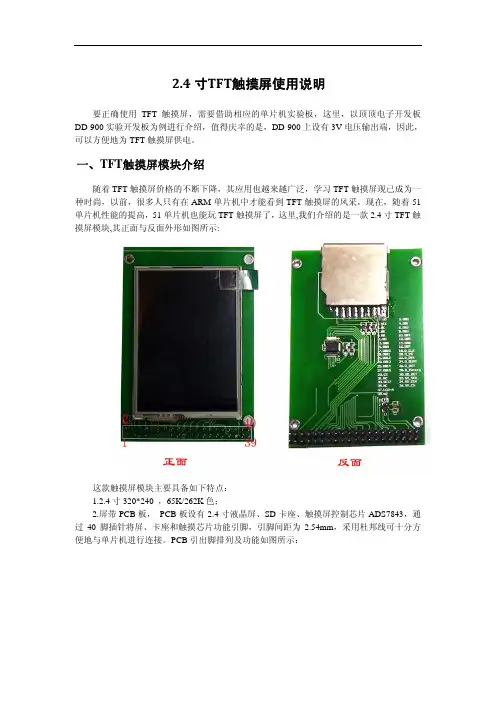
TFT 触摸屏模块介绍随着TFT 触摸屏价格的不断下降,其应用也越来越广泛,学习TFT 触摸屏现已成为一种时尚,以前,很多人只有在ARM 单片机中才能看到TFT 触摸屏的风采,现在,随着51单片机性能的提高,51单片机也能玩TFT 触摸屏了,这里,我们介绍的是一款2.4寸TFT 触摸屏模块,其正面与反面外形如图所示:这款触摸屏模块主要具备如下特点:1.2.4寸320*240 ,65K/262K 色;2.屏带PCB 板, PCB 板设有2.4寸液晶屏、SD 卡座、触摸屏控制芯片ADS7843,通过40脚插针将屏、卡座和触摸芯片功能引脚,引脚间距为2.54mm ,采用杜邦线可十分方便地与单片机进行连接。
PCB 引出脚排列及功能如图所示:3.屏设置为8位,用户也可根据实际情况设置为16位。
4.控制IC 为ILI9325。
二、供电及连接说明DD-900实验开发板采用的是5V 供电,因此,单片机应采用5V 单片机,如STC89C516RD+、STC12C5A60S2等,晶振采用30M ,注意TFT 要采用3V 供电,否则有可能烧屏,TFT 与单片机连接时可加限流电阻,电阻大小为470欧左右,也可以不加,但单片机不可设置为推挽模式,各引脚连接如下: TFT 触摸屏 DD-900实验开发板 说明 GND GND 屏与背光供电VCC 3V LED+ 3V DB8~DB15 P00~P07 液晶屏部分DB0~DB7不连接(这里采用是8位方式,不用连接)RS P26 WR P25 RD P24 CS P27 RES P23 D_CLK P21 触摸控制部分D_CS P20 D_DIN P22 D_BUSY P34 D_DOUT P33 D_Penirq (中断) P35 SD_OUT 根据程序进行定义 SD 卡座部分(前两个实验,此部分未采用) SD_SCK 根据程序进行定义SD_DIN根据程序进行定义SD_CS 根据程序进行定义注意:在TFT 的PCB 板上标有TFT 的引脚功能,一定要认清管脚与标注的对应关系。
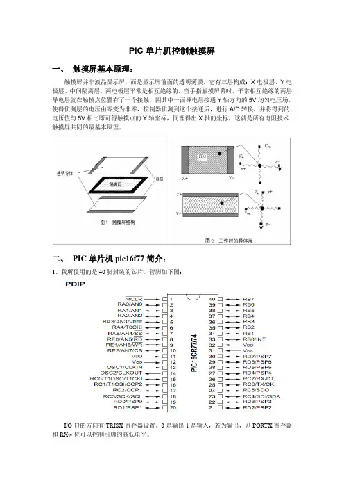
PIC单片机控制触摸屏一、触摸屏基本原理:触摸屏并非液晶显示屏,而是显示屏前面的透明薄膜。
它有三层构成:X电极层、Y电极层、中间隔离层。
两电极层平常是相互绝缘的,当手指触摸屏幕时,平常相互绝缘的两层导电层就在触摸点位置有了一个接触,因其中一面导电层接通Y轴方向的5V均匀电压场,使得侦测层的电压由零变为非零,控制器侦测到这个接通后,进行A/D转换,并将得到的电压值与5V相比即可得触摸点的Y轴坐标,同理得出X轴的坐标,这就是所有电阻技术触摸屏共同的最基本原理。
二、PIC单片机pic16f77简介:1、我所使用的是40脚封装的芯片。
管脚如下图:I/O口的方向有TRISX寄存器设置。
0是输出1是输入,若为输出,则PORTX寄存器和RXw位可以控制引脚的高低电平。
2、AD转换模块:AD转换模块有三个寄存器:ADCON0、ADCON1、ADRES。
AD转换的步骤:其中第4步中需要等待的采集时间有时不能按照文档中所说的16us左右。
如果单纯的用一路AD通道,则16us的采集时间是可以的。
但是若涉及到多通道之间的相互转换后,这个时间就不能保证采集的信号是正确的,应该延长采集时间。
我看到网上有人说用1ms 的延时,具体延时应根据实际情况测量一下。
AD转换结果位于ADRES寄存器中,8位。
3、通用串口USART:建议大家调试程序的时候多用一下USART,太好用了。
下面是有关寄存器:TXREG :发送缓冲器,RCREG :接收缓冲器。
4、中断:下面是与中断有关的寄存器:中断编程需要注意的问题:PIC单片机的编程软件是MPLAB,它只有一个中断函数,并且有interrupt关键字。
多个中断同时使能时,需要在中断函数里判断中断标志位,来判断是哪个外设发生了中断。
三、控制电路:程序设计:(1)、检测是否有触控操作:首先使T1、T3导通,T2、T4截止,AD转换ADY 的电压值,若为0或某一范围内,则认为没有触控操作,否则有触控操作。
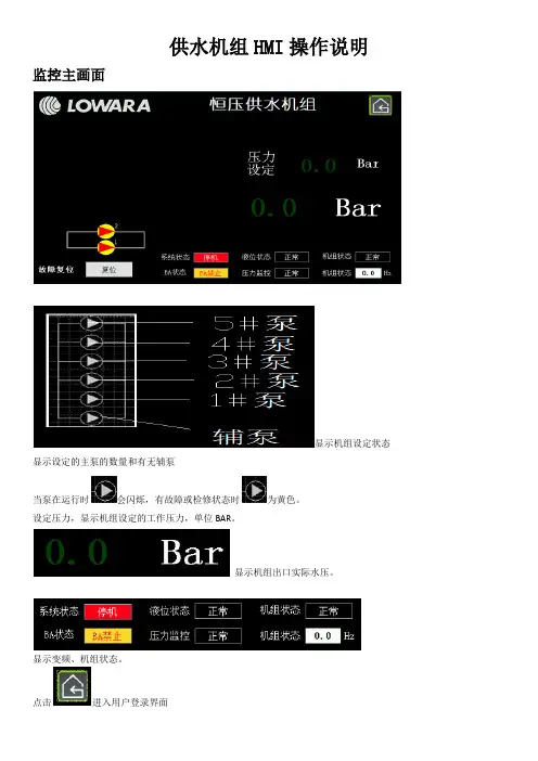
供水机组HMI操作说明监控主画面显示机组设定状态显示设定的主泵的数量和有无辅泵当泵在运行时会闪烁,有故障或检修状态时为黄色。
设定压力,显示机组设定的工作压力,单位BAR。
显示机组出口实际水压。
显示变频、机组状态。
点击进入用户登录界面点击进入输入用户名:“8”。
点击设定用户密码“88888888”,设定完成点击密码:输入8个8,完成确定。
“”。
密码正确点击,进入机组参数设定界面:按上图所示,设定系统所需压力、主泵数量、压力传感器量程。
点击进入PID参数设定界面。
点击可将PID设定成手动或自动/正常为自动。
上面参数为PID的比例,积分时间,微分时间三个参数。
正常按系统初始值设定,可微小调整。
按界面显示设定其他参数,正常不需要调整。
点击进入水泵控制界面加载,变频运行的水泵运行到加泵频率之上,压力仍然小于系统设定压力减去加泵偏差加泵延时,上述条件满足后,经过加泵延时时间后,系统进行加泵操作。
减载,同上原理。
用户可能调整参数1,变频状态加载延时当变频泵升到49HZ且压力低于设定压力时,延时设定的时间后将变频泵变为工频运行,未运行的泵变为变频。
2,变频状态减载延时当变频泵的频率降到35HZ时,压力高于设定值,延时时间到后,将停止工频泵,先启先停的原理。
需要有变频工作变为工频运动的水泵启动的延时时间,单位秒。
未运行的水泵由停止变为变频运行的延时时间,单位为秒。
可设定系统是否允许机组进入休眠。
进入休眠条件:1,已启用休眠功能2,变频运行频率<3,机组实际压力>机组设定压力-休眠压力偏差4,机组只有1台泵正在变频运行,无工频运行。
5,以上4条同时满足且满足实际时间大于“进入休眠延时”休眠唤醒条件,1,机组实际压力<机组设定压力2,条件1满足且满足时间>休眠唤醒延时时间休眠瞬间唤醒条件,机组实际压力<机组设定压力+瞬时唤醒偏差。
其他参数界面,显示个水泵状态及故障复位。
点击按钮可切换水泵状态,工作或检修,当水泵的状态为检修时,其不参与机组自动控制。
TI StellarisWare图形库使用指南[V1.0][作者: Richard Ma][Email: mxschina@]1.前言 (1)2.基础知识 (2)2.1.显示驱动层 (Display Driver Layer) (2)2.1.1.基本功能 (2)2.1.2.图形输出驱动 (3)2.1.3.用户输入驱动 (3)2.2.基本图形层 (Graphics Primitives Layer) (4)2.3.控件层 (Widget Layer) (4)3.StellarisWare图形库基本使用 (6)3.1.开发环境及StellarisWare安装 (6)3.2.图形库添加与编译 (显示部分) (7)3.2.1. 建立新项目 (7)3.2.2. 添加图形库 (8)3.2.3. 驱动程序初始化 (10)3.3.图形库添加与编译 (触摸部分) (10)4.基本图形绘制 (12)4.1. 绘图上下文 (tContext) (12)4.2. 颜色设置 (12)4.3. 绘制基本图形 (13)4.4. 绘制文字 (14)4.5. 绘制图片 (16)4.5.1. 图片表示方式 (16)TI StellarisWare图形库使用指南 Richard Ma4.5.2. 图片生成工具 (17)5.控件使用 (19)5.1. 控件使用示例代码 (19)5.2. 控件使用步骤说明 (23)5.2.1. 配置显示及用户输入 (24)5.2.2. 创建控件及属性配置 (24)1)控件名 (25)2)控件管理–控件树 (25)3)显示设备对象(pDisplay) (27)4)位置和尺寸 (27)5)控件风格(Style)及其它属性 (27)6)事件响应 (27)5.2.3.控件添加绘制及管理 (28)6.各控件功能及属性 (29)6.1. 画布控件(Canvas) (29)6.2. 选择/多选框控件(Checkbox) (33)6.3. 容器控件(Container) (36)6.4. 图形按钮控件(Image Button) (39)6.5. 列表框控件(ListBox) (43)6.6. 按钮控件(Push Button) (46)6.7. 单选按钮控件(Radio Button) (51)6.8. 拖滑/进度条控件 (Slider) (54)1.前言TI Stellaris系列Cortex-M3/Cortex-M4F系列MCU的方便强大,StellarisWare软件库提供的快速软件开发解决方案功不可没。

Veriti PCR仪简明操作说明Applied Biosystems触摸屏常用按键说明:操作步骤:1、打开PCR仪的热盖,插入样品管。
盖好热盖。
2、打开PCR仪的电源,仪器程序开始初始化,需等待几分钟。
3、初始化完成后,显示主菜单:4、点“Browse/New Methods”,进入PCR程序列表:5、可以直接点一个PCR程序,选择“Start Run”运行;点右边的符号,可以选择不同的文件夹。
如要新建一个PCR程序,点“New”,出现PCR程序:6、添加一段程序:点中上方的“Stage”位置,该位置变红;再点“Add”,软件将加入一段新的程序。
7、修改循环数、温度、时间:点中循环次数、温度或时间位置,下方出现数字键。
依次点数字键,出现合适数字后,点“Done”确定。
8、增加一个步骤:点“Step”位置,该位置变红;再点“Add”,软件将加入一个新的步骤。
9、删除一个步骤:点“Step”位置,在点“Delete”,软件将该步骤删除。
10、建立梯度模式:1)点中一个步骤,再点“Option”键,出现选项如下2)点“VeriFlex step”,出现梯度创建窗口:输入6个梯度温度,温度下方的“1-2”是指对应的1、2两行加热孔,全部输好后,点“Done”确定。
注意:相邻的两个梯度温度之差最大不能超过5℃!11、建立渐变模式:1)点中一个步骤,再点“Option”键,出现选项如下2)点“Auto Delta”,出现渐变模式创建窗口。
点“Staring Cycle”,输入起始循环数;点“Delta Temperature”,输入温度变化值;点“Delta Time”,输入时间变化值。
渐变模式适用于touchdown PCR,可以提高PCR反应的特异性。
例:输入起始循环数为2,温度变化值为+0.5℃,时间变化值为+5s,则表示从第2个循环开始,每循环一次升温0.5℃,时间增加5s。
12、增加暂停步骤:1)点中一个步骤,再点“Option”键,出现选项如下3)点“Pause”,出现如下窗口。
触摸屏控制芯片ADS7843中文资料当触笔触到屏上时,对应的位置就会产生相应大小的电压,输入到芯片,AD 转换后得到一个数据。
而触摸校准就是将接受到的原始模数转换值转换成屏幕像素坐标。
再就是了解触摸芯片,知道他的工作方式,以及跟STM32的连线。
触摸实验中,我的实验板是用SPI口来实现数据的传输的,即SPI与xpt2046相连。
触摸屏控制芯片ADS7843中文资料ADS7843是一个内置12位模数转换、低导通电阻模拟开关的串行接口芯片。
供电电压2.7~5 V,参考电压VREF为1 V~+VCC,转换电压的输入范围为0~ VREF,最高转换速率为125 kHz。
ADS7843引脚图及引脚功能说明了:ADS7843的引脚配置如图3所示。
表1为引脚功能说明,图4为典型应用。
ADS7843典型应用电路ADS7843之所以能实现对触摸屏的控制,是因为其内部结构很容易实现电极电压的切换,并能进行快速A/D转换。
图5所示为其内部结构,A2~A0和SER/为控制寄存器中的控制位,用来进行开关切换和参考电压的选择。
ADS7843之所以能实现对触摸屏的控制,是因为其内部结构很容易实现电极电压的切换,并能进行快速A/D转换。
图5所示为其内部结构,A2~A0和SER/为控制寄存器中的控制位,用来进行开关切换和参考电压的选择。
2.3 ADS7843的控制字及数据传输格式ADS7843的控制字如表4所列,其中S为数据传输起始标志位,该位必为"1"。
A2~A0进行通道选择(见表2和3)。
MODE用来选择A/D转换的精度,"1"选择8位,"0"选择12位。
SER/选择参考电压的输入模式(见表2和3)。
PD1、PD0选择省电模式:"00"省电模式允许,在两次A/D转换之间掉电,且中断允许;"01"同"00",只是不允许中断;"10"保留;"11"禁止省电模式。
觸摸屏驅動芯片列表
1、2046 是4线式触摸屏控制器ADS7846的替代产品,支持1.5V~5.25V低压I/O界面,与现有的ADS7846 可实现100%的PIN to PIN 替换,使用相同的插座产品特性:
2.2V TO 5.25V 工作电压范围
1.5V TO 5.25V 数字输入输出
内置2.5V 参考电压
直接电池电压检测功能(0V to 6V)
片上温度检测功能
触摸压力检测功能
QSPITM 和SPITM 3-WIRE 界面
自动掉电保护功能
QFN-16封装
可应用于:
手机
PDA 个人数字助理
便携式设备
自动销售终端
寻呼机
触摸屏监控器
蜂窝电话
2、TSC2003是TI公司生产的采用TSSOP一16封装的四线电阻式触摸屏控制芯片,集成了多个功能模块,具有测量电量、片上温度和触摸压力等功能,通过I2C总线与单片机连接。
TSC2003是一款基于命令控制的触摸屏检测器件,通过I2C总线发送控制命令来控制芯片采集X轴、Y轴和Z轴的压力等相关量。
3、触摸屏驱动IC UH7843可完全替换TCS2046 AR7643及AKM4812 特点:4 wire Touch Panel interface,12-bit analog to digital converter up to 125KHZ conversion,SSOP-16 QFN-16以及客户要求的封装
PIN TO PIN 。
4、。

敦泰TP IC 调屏步骤一、关掉自动调屏,找到文件FLOWWORK.C中的查找CHIPCLB,屏掉,调完后在打开。
二、调屏基本参数,在GLOBAL CONFING.H,中修改1,先选择一种芯片,如FT5406,屏掉不用的芯片型号,如 #define FT54062,接口定义,如i2c接口,#define IICEN。
3,如果定义为i2c接口,要选择一种通信协议,如标准i2c和26字节,#define CFG_SUPPORT_COM_I2C_PROTOCOL 1 //~1:STD PROTOCOL, 0:FTPROTOCOL,1=标准i2c协议,0=26字节协议。
4,中断io口电压选择,如0=0~3.3V(客户的电压为3.3v和3.0v及2.8v时选此项),1=1~1.8V(客户的电压1.8v时选此项),如#defineIO_LEVEL_SELECTION 0 //0---3.3v; 1----1.8v 5,设置器件地址,如0x70,#define I2C_SLAVE_ADDR 0x70 //Device addresses top 7 bits6,据据芯片型号改Tx Order,rx Order通道数目和调整通道顺序,#define NUM_TX_LOCAL 28 // TX number of CTP7,设置触模点数,如5点,#define CURRENT_NUMBER_SUPPORTED 5 //The maximum number of output coordinates8,找TX_CAP_VALUE and RX_CAP_VALUE的极值(找极值的方法,请看调屏指南)#define TX_CAP_VALUE{64,64,64,64,64,64,64,64,64,64,64,64,64,64,64,64,64,64,64,64,64,64,64,64,64,64, 64,64}//在开始调试时设为默认值如64.#define RX_CAP_VALUE{128,128,128,128,128,128,128,128,128,128,128,128,128,128,128,128}//在开始调试时设为默认值如128.9,设置电荷泵的电压The chargepump value,Chip Vol可设为默认值如=2,如ft5406时,3.3V供电,有8个档,0=6.75v~8=5v10, 调整TX_OFFSET_VALUE和RX_OFFSET_VALUE的值,目标使rawdata=8500(+-300).#define TX_OFFSET_VALUE{0x33,0x33,0x33,0x33,0x33,0x33,0x33,0x33,0x33,0x33,0x33,0x33,0x33,0x33}//在开始调试时设为默认值如0x33.#define RX_OFFSET_VALUE {0x55,0x55,0x55,0x55,0x55,0x55,0x55,0x55}//在开始调试时设为默认值如0x55.注意TX_OFFSET_VALUE和RX_OFFSET_VALUE值的高4位和低4位分配,请看调屏指南。
老虎触屏控台说明书Tiger Touch Operator’s Manual Version 3.0 1 控台设置 (8) 1.1 控台向导 (8)1.2 连接 (12)1.2.1主电源连接 (12)1.2.2启动与关闭 (12)1.2.3 连接DMX线 (12)1.2.4连接一个VDU(视频显示器) (13) 1.2.5其他连接 (13) 1.3 使用触摸屏和VDU(视频显示器) (14) 1.3.1工作窗口 (14) 1.3.2 触摸屏菜单区 (16)1.3.3 工具栏 (18)1.3.6 按键功能配置文件 (21)1.3.7 宏按键功能 (22)1.3.8 Tiger Touch Titan的应用 (22)1.4 读取和保存show (23)1.4.1手动保存和加载 (23)1.4.2自动保存 (24)1.4.3 备份现有的文件在U盘 (25)1.5 清除控制台 (25)2.配接 (26)2.1创建 (26)2.1.1灯具选择按键 (26)2.1.2 配接常规灯(Dimmer) (27)2.1.3 配接电脑灯 (28)2.1.4 Visualiser自动配接 (30)2.2 编辑 (30)2.2.1. 更改电脑灯的DMX地址 (30)2.2.2 命名 (31)2.2.3 查看配接 (32)2.2.4灯具调换(Fixture Exchange) (33) 2.2.5 更新灯库文件 (34) 2.3 复制和移动 (34)2.3.1 复制或移动配接的电脑灯 (34) 2.3.2 使用复制灯具 (35) 2.4 删除 (36)2.4.1 删除一个已配接的电脑灯 (36) 2.5 高级选项 (36)2.5.1 调换水平和垂直功能 (36)2.5.2 反转属性 (37)3. 控制常规灯和电脑灯 (38)3.1 创建 (38)3.1.1 选择灯具来控制 (38)3.1.2 设置灯具的开始位置 (39)3.1.3 清除选择按键 (40)3.1.4 更改控制轮的属性 (41)3.1.5使用触摸屏设置属性 (43)3.1.6 使用数字设置属性 (44)3.1.7 通过数字选择fixtures和dimmers (45)3.1.8 模式选择(Selecting using a pattern) (46)3.1.9 属性组–IPCGBES (47)3.1.10 灯具编组(group) (47)3.1.11 步进式一次选择一个灯具 (49)3.1.12 选择灯具输出高亮状态 (49)3.1.13 排列灯具(Align) (49)3.1.14 翻转(Filp) (50)3.1.15 扇形散开(Fan)模式 (50)3.2 编辑 (51)3.2.1 网格通道窗口 (51)3.3 高级选项 (52)3.3.1 Tools/Menu Latch按键 (52)4.素材(Palettes) (53)4.1 创建 (53)4.1.1 素材以相对值保存 (53)4.1.2 哪个属性存储到素材中 (54)4.1.3保存一个素材 (54)4.1.4 快速保存 (56)4.2 重放 (56)4.2.1. 调出一个素材值 (56)4.2.2素材页面 (57)4.2.3 快速素材 (57)4.2.4 在一个重放中设置素材到灯具 (57)4.3. 编辑 (58)4.3.1.编辑素材 (58)4.3.2. 命名素材 (58)4.4 复制和移动 (59)4.4.1 复制或移动一个素材 (59)4.5 删除 (60)4.5.1 删除素材 (60)4.6 时间 (60)4.6.1 渐变(fade)一个素材和灯具交叠(fixture overlap) (60)4.6.2 素材主控时间(Master Time) (61)5.内置效果(Shapes) (62)5.1 重放 (63)5.1.1 创建一个内置效果 (63)5.1.2 修改内置效果的大小和速度 (64)5.1.3 在多个灯具中扩散内置效果 (65)5.2 编辑 (67)5.2.1 编辑运行中的内置效果 (67)5.2.2 反转内置效果 (67)5.3 删除 (67)5.3.1 删除内置效果 (67)5.4 高级选项 (68)5.4.1 内置效果的淡入淡出模式 (68)6. Cues (69)6.1创建 (69)6.1.1 编程时Tiger Touch如何工作 (69)6.1.2 创建一个cue (70)6.1.3 在cue中使用图形 (71)6.2重放 (71)6.2.1 HTP和LTP (72)6.2.2 重放一个cue (72)6.2.3 更改重放页面 (73)6.2.4释放运行的重放 (73)6.3编辑 (74)6.3.1 编辑一个cue (74)6.3.2 查看cue和重放 (75)6.3.3调入(Include)功能 (76)6.3.4 使用“Off”从cue中移除一个属性 (77) 6.4 复制,移动和链接 (78)6.4.1复制或移动一个cue (78)6.5 删除 (79)6.5.1.删除一个cue (79)6.6 时间 (79)6.6.1 为一个cue设置渐变时间和交叠 (80) 6.6.2 改变灯具顺序 (82)6.6.3 为一个cue设置属性的渐变时间 (83) 6.7 高级选项 (84)6.7.1 释放遮盖 (84)6.7.2 推杆控制图形的大小/速度 (85)6.7.3 曲线 (85)6.7.4 手柄页面锁定(Handle Paging) (85) 6.7.5 重放优先级别 (85)6.7.6 按键功能配置文件(Key Profile) (86)7. 多步程序(Chase) (87)7.1 创建 (87)7.1.1 编辑一个多步程序(chase) (87)7.2 重放 (88)7.2.1 运行一个多步程序 (88)7.2.2 连接一个多步程序到控制台 (89)7.2.3 设置多步程序的速度,交叉淡入淡出(crossfade) (90)7.2.4 手动控制多步程序的步 (90)7.2.5 改变多步程序的方向 (91)7.2.6 跳到一个步 (91)7.3 编辑 (91)7.3.1 打开编辑一个多步程序 (91)7.3.2 用 Unfold(展开)编辑一个多步程序 (92)7.4 复制,移动和连接 (93)7.4.1 复制或者移动一个多步程序 (93)7.5 删除 (94)7.5.1 删除多步程序 (94)7.5.2 从多步程序中删除一个步 (94)7.6 时间 (95)7.6.1 设置多步程序中global的时间 (95)7.6.2 设置时间并且关联到单独的步 (96)7.6.3 设置属性淡入淡出的时间并且关联到单独的步 (98) 7.7 高级选项 (99)7.7.1 循环/停止一个cue (99)7.7.2 向前/向后/退回/随机 (99)7.7.3 步的链接 (99)7.7.4 记住cue (99)8. Cue Lists (100)8.1 创建 (101)8.1.1 编程一个 cue list (101)8.1.2 为cue list中的cue重命名 (102)8.1.3 在一个cue list中自动加载一个重放 (103)8.2 重放 (104)8.2.1运行一个cue list (104)8.2.2 快速终止(kill)一个 cue list (105)8.3 编辑 (105)8.3.1使用展开(Unfold)编辑一个cue list (105)8.3.2 编辑一个正在运行的 cue list (106)8.3.3 编辑一个正在记录的cue list (107)8.4 复制,移动和链接 (108)8.4.1复制或移动一个cue list (108)8.5 删除 (109)8.5.1.删除cue list (109)8.5.2 删除cue list中的一个cue (109)8.6 时间 (110)8.6.1 Cue List的时间和重放选项 (110)8.6.2 Cue链接和链接反转(Link Offset) (111)8.6.3 设置属性的渐变时间 (113)8.6.4 灯具交叠(Fixture Overlap) (113)8.6.5 使用时间码运行一个cue list (114)8.7 高级选项 (115)8.7.1 释放遮盖 (116)8.7.2 推杆工作模式(Fader mode) (116) 8.7.3手柄页面锁定(Handle Paging) (116) 8.7.4 Cue选项 (117)8.7.5 自动加载 (117)8.7.6按键功能配置文件(Key Profile) (117)9. 运行演出(Running the show) (118)9.1 重放 (118)9.1.1 备份show (118)9.1.2 工作模式 (118)9.1.3 主控推杆(Master fader) (118)9.1.4 Flash 和 swop 按键 (119)9.1.5 重放优先 (119)9.1.6 预置重放 (119)9.1.7 手动控制show (120)9.2 触摸屏和视频显示工作区 (121)9.2.1 查看菜单 (121)9.2.2 Tiger Touch Titan应用窗口 (121)9.3 使用移动功能 (122)10. 遥控 (123)10.1 设置遥控 (123)10.1.1 网络设置(Network setup) (124) 10.1.2 控台设置 (125) 10.2 操作遥控 (126)10.2.1 键盘 (126)10.2.2 灯具列表 (128)10.2.3 重放列表 (129)10.2.4 设置屏幕 (129)10.3 故障检测(Troubleshooting) (130)11. 用户设置和其他选项 (131)11.1 配置工作窗口 (131)11.1.1 打开工作窗口 (131)11.1.2 选择和定位工作窗口 (131)11.1.3 保存工作窗口 (132)11.1.4 兼容性视图 (133)11.1.5 配置外接显示器 (134)11.2 按键概况 (135)11.2.1 创建和编辑按键 (136)11.2.2 选择一个键设置 (137)11.2.3 单个重放键设置 (137)11.3 系统菜单 (138)11.3.1 Avotalk安全 (138)11.3.2 网络设置 (138)11.3.3 用户设置 (138)11.3.4 键设置 (139)11.3.5 清除 (139)11.3.6 显示设置 (140)11.4 VDU工具菜单 (140)11.4.1 Virtual面板 (140)11.4.2 Visualiser (140)11.4.3 VDU(视频显示器)用户设置 (140)11.4.4 出厂设置 (142)11.4.5 交换灯具 (143)11.4.6 设置DMX输出口 (143)11.4.7 热键功能 (143)11.5 曲线 (143)11.6 升级软件 (145)11.7 恢复/重新安装系统 (146)11.7.1 USB恢复棒引导 (146)11.7.2 安装说明 (147)11.7.3 安装以后 (147)11.7.4 前面板按键BOIS映射 (148)12. 灯库文件(Fixture Personalities) (149)12.1.1 从Avolite网站上下载灯库文件 (149)12.1.2 在控台上更新的灯库文件缓存区(Cache) (150) 12.1.3 申请一个新的的灯库文件 (151)12.1.4 向Avolites报告灯库错误 (151)12.1.5 在紧急情况下 (151)13. 网络 (153)13.1 设置Tiger T ouch IP地址 (153)13.1.1 设置IP地址 (153)13.2 设置DMX输出 (154)13.2.1 DMX输出安装窗口 (155)13.3 ArtNet (156)13.3.1 一个简单的ArtNet系统 (156)13.3.2 设置一个Art Net 系统 (158)13.3.3 附加Artnet资源 (159)13.4 用ACDI(异步通讯设备接口)连接模拟器(160) 13.4.1 ACDI (160)13.5 模块设置 (161)13.5.1 安装额外的模块 (162)13.6 AvoTalk (162)13.7 有关IP地址内容 (162)13.7.1 设置你的IP地址 (163)13.7.2 子网掩码 (164)13.7.3 选择一个IP地址和子网掩码 (164)13.7.4 自动分配IP地址(DHCP) (165)13.7.5专用IP地址范围 (166)13.8修复网络连接 (166)14. Tiger Touch用户说明 (167)14.1 控制和屏幕 (167)14.2 新的编程功能 (169)15. 版本备注(Release notes) (171)16. 术语表(Glossary of terms) (171)1 控台设置本章提要:连接主电源,DMX 信号线,视频显示;控台配置和各种视频显示窗口;控台向导;加载和保存show 。
触屏泰克示波器操作手册
触屏示波器操作手册(Touchscreen Oscilloscope User Manual)
本操作手册为用户提供了触屏示波器的详细操作指南。
请您仔细阅读本手册,并按照其中的步骤进行操作。
目录:
1. 引言
1.1 示波器简介
1.2 触屏示波器简介
1.3 本手册目的
2. 触屏示波器概述
2.1 触屏功能简介
2.2 示波器界面概览
2.3 主要控件介绍
3. 示波器操作
3.1 示波器开机与关机
3.2 屏幕操作
3.2.1 单指滑动
3.2.2 双指缩放
3.2.3 多指旋转
3.3 输入信号设置
3.4 触发设置
3.5 垂直(Y)设置
3.6 水平(X)设置
3.7 光标测量
4. 仪器维护与安全
4.1 仪器清洁与保养
4.2 仪器安全事项
4.3 故障排除与维修
附录:
A. 命令指令列表
B. 常见问题与解答
C. 技术规格与参数
请注意,本操作手册仅适用于特定型号的触屏示波器,不同型号可能存在差异,请您按照实际情况进行操作。
如有任何问题或疑问,请联系我们的技术支持人员。
触摸屏控制实验设计报告序随着中国工业化的快速发展,对工业自动化控制的要求也在不断提高和完善。
触摸屏作为一种可视化的人机界面,以其体积小、可靠性高的特点逐渐取代传统的按钮控制和仪表控制,成为工业控制中人机界面的主流。
本文分析了触摸屏设备的特点、国外现状和发展趋势,设计了一种基于嵌入式实时操作系统WinCE5.0和ARM9系列AT91SAM9261为核心处理器的大型触摸屏控制器。
考虑到触摸屏设备的功能需求,提出了本课题的设计指标,制定了触摸屏控制器的总体设计方案,具体体现在控制器硬件设计和操作系统移植两个方面。
硬件平台采用模块化、结构化的思想进行设计和实现。
分析了触摸屏控制器中的主要硬件模块,包括处理器核心模块、存储模块、触摸屏模块、键盘模块、以太网模块和USB主从模块,并给出了硬件设计方法和电路实现。
硬件测试环境的建立是为了调试我弟弟的硬件模块。
基于搭建的硬件平台,本文重点研究了嵌入式操作系统WinCE 5.0的移植和BSP的开发。
分析了WinCE 5.0操作系统的架构和移植原理,在了解了三星公司的S3C2410 BSP之后,给出了基于AT91SAM9261的WinCE 5.0 BSP的开发过程。
详细分析了WinCE 5.0 Bootloader的工作原理和体系结构。
根据触摸屏系统的功能需求和硬件资源的分配,设计了触摸屏设备的Bootloader,并给出了具体的开发步骤。
深入研究了OAL的功能和原理,详细给出了OAL开发中的重要功能和主要模块。
针对触摸屏控制器的主要硬件模块,在分析WinCE 5.0中断模型和中断机制的基础上,开发了触摸屏驱动程序、矩阵键盘驱动程序和USB主机驱动程序。
在开发的BSP的基础上,利用WinCE 5.0操作系统定制工具Plarform Builder 对操作系统内核进行定制和编译,并对操作系统的性能进行测试。
测试结果表明,WinCE 5.0操作系统能够成功移植到触摸屏控制器上,能够满足工业现场的实时性要求。
可编辑修改精选全文完整版目录1.互动教学屏操作 (2)1.1开机操作 (2)1.2信号切换操作 (2)1.3键盘鼠标操作 (2)2.互动教学展台软件操作 (3)3.无线互动操作 (3)4.安卓系统操作 (4)5.关机操作 (4)8.常见问题解答 (4)1.互动教学屏操作1.1开机操作1、教室的配电箱——打开总电源2、屏幕下方TV指示灯变“红灯”3、按屏幕下方“待机”键——TV指示灯变“蓝灯”,显示屏已打开。
4、按“电脑”键——PC指示灯亮“蓝灯”,内置电脑已打开。
配电箱图屏幕前端按键图1.2信号切换操作⏹屏幕前端按键:第一步:按“信号键”,显示切换菜单。
信号菜单图第二步:按“频加键”或“频减键”进行选择。
第三步:按“音加键”确定选项遥控器操作键图1.3键盘鼠标操作⏹触控鼠标:双击打开程序,长按2秒为鼠标右键。
⏹触控键盘:轻触侧面调出键盘。
⏹无线键鼠:接收端接入USB口,打开键盘和鼠标开关。
2.互动教学展台软件操作画笔1自动对焦画面移动PowerPoint 支援画笔2 亮度+/-功能全部删除电脑操作模式视频录制画笔设定图像反転隐藏功能视频展台模式电脑批注模式下一个菜单保存教材读取模式白板模式选择返回结束缩放+/-画面冻结区块强调3.无线互动操作无线互动连接:1、将无线发射棒与笔记本或PAD上的HDMI口和USB口连接。
2、将信号源切换到“无线互动”,即可显现屏幕内容。
3、将触控开关拨到第1档,即可实现屏幕触控。
无线发射端图4.安卓系统操作安卓系统操作:1、将信号源切换到“多媒体互动”,即可显现屏幕内容。
2、将触控开关拨到第3档,即可实现屏幕触控。
3、将U盘或SD卡插入,即可实现PPT、WORD、音视频等课件播放。
4、接入网线即可上网下载文件。
5、将网络设置在同一局域网下,可以分享安卓手机或PAD上的图片、音频和视频。
安卓系统接口图5.关机操作⏹互动教学屏先正常关闭电脑,待PC指示灯熄灭后,再关闭显示器,待TV指示灯由蓝灯变为红灯。
TPD-283-H 2.8” TouchPAD - QuickStart (Dec/2017)ICP DAS USA, Inc. | | 1-310-517-9888 | 24309 Narbonne Ave. Suite 200. Lomita, CA 907171TPD-283-H2.8'' High Speed Touch Screen HMI ControllerQuick Start GuideProduct Website:https:///tpd_283_h.html1. IntroductionThis quick start manual will guide users to implement the TPD-283-H module into their applications in a quick and easy way. This will only provide with the basic instructions. For the more detailed information, please refer to the TPD-283-H user’s manual located on the ICPDAS CD-ROM or from ICP DAS web site :https:///documents/user-manual-TPD-283-H.pdfThe ICP DAS TouchPAD is a tiny touch screen controller (electrical switch) HMI which is designed for building and home automation. TPD-283U-H is equipped with a high resolution TFT color touch screen and fits in regular electrical wall-mount outlets.TPD-283-H 2.8” TouchPAD - QuickStart (Dec/2017)ICP DAS USA, Inc. | | 1-310-517-9888 | 24309 Narbonne Ave. Suite 200. Lomita, CA 9071722. WiringsTPD-283-H 2.8” TouchPAD - QuickStart (Dec/2017)ICP DAS USA, Inc. | | 1-310-517-9888 | 24309 Narbonne Ave. Suite 200. Lomita, CA 907173TPD-283-H 2.8” TouchPAD - QuickStart (Dec/2017)ICP DAS USA, Inc. | | 1-310-517-9888 | 24309 Narbonne Ave. Suite 200. Lomita, CA 9071743. Install HMIWorksFollow the steps to install the HMIWorks.4. Setup DeviceStep1. Before downloading programs to the TPD-283U-H, be sure to setup TPD-283U-H first. Run HMIWorks_Standard.exe and click on the menu: Run >> Setup Device.TPD-283-H 2.8” TouchPAD - QuickStart (Dec/2017)ICP DAS USA, Inc. | | 1-310-517-9888 | 24309 Narbonne Ave. Suite 200. Lomita, CA 907175Step 2. In the “Setup Ethernet device” dialog box, click the “search for TouchPAD” button to open “search for TouchPAD” dialog box.TPD-283-H 2.8” TouchPAD - QuickStart (Dec/2017)ICP DAS USA, Inc. | | 1-310-517-9888 | 24309 Narbonne Ave. Suite 200. Lomita, CA 907176Step 3: If the TouchPAD device is found and displayed in the list on the “Search for TouchPAD” dialog box, select the TouchPAD item depend on MAC Address of your TouchPAD device and click the “OK” button to bring the information back to the “Setup Ethernet Device” dialog box.Note: You can find the MAC address on the back of the TouchPAD.TPD-283-H 2.8” TouchPAD - QuickStart (Dec/2017)ICP DAS USA, Inc. | | 1-310-517-9888 | 24309 Narbonne Ave. Suite 200. Lomita, CA 907177Step 4: In the “Setup Ethernet Device” dialog box, select the “DHCP”,“Static IP” or “Runtime Setting” (e.g., DHCP) in the “IP Address Assignment Method” field. Notes:1. When using “Static IP” or “DHCP”, the IP settings are stored as a part of the program image, and only successful downloading can update the IP settings.2. When using “Runtime Setting”, the program image has no information about the IP settings, and TouchPAD loads the IP information from the flash at the runtime. Before IP settings are used, be sure to set the IP settings into the flash by the related API functions. We have demo to do this as well.TPD-283-H 2.8” TouchPAD - QuickStart (Dec/2017)ICP DAS USA, Inc. | | 1-310-517-9888 | 24309 Narbonne Ave. Suite 200. Lomita, CA 907178Step 5: Verify that “Host IP Address” and “TouchPAD IP Address” in the same subnet.Step 6: Verify that “TouchPAD MAC Address” must match the MAC Address of your TouchPAD device, and click the “OK” button.Note: Verify that the new project has been created (see Section 3.2 “Create a New Project in the HMIWorks”).TPD-283-H 2.8” TouchPAD - QuickStart (Dec/2017)ICP DAS USA, Inc. | | 1-310-517-9888 | 24309 Narbonne Ave. Suite 200. Lomita, CA 907179Step 7: Click the “Run (Build & Download) F9” item from the “Run (Build & Download)” menu, or press F9.Step 8: The “Download in progress…” dialog box will be displayed showing the progress of the update.Step 9: The TouchPAD device will then execute the string “Hello TouchPAD!” sample.。
控制器的触摸屏操作指南控制器的触摸屏操作是现代智能化设备的核心之一,因此,掌握正确的操作技巧和方法非常必要。
本文将向您介绍一些关于指导控制器的触摸屏操作的技巧和方法。
一、控制器触摸屏操作基础在学习任何设备的操作之前,初学者都需要掌握一些基本的操作技巧。
控制器的触摸屏也不例外。
首先,用户应该熟悉触摸屏上的各种按钮、选项和图标,以便更好地了解设备的功能和操作流程。
其次,用户应该知道如何进行单点触摸、双点触摸、长按等基本手势操作。
此外,用户还应该学会如何使用菜单选项、输入框、列表等控件。
二、操作指南1. 触摸屏幕:在开始使用控制器之前,您需要确认是否已开启触摸屏。
如未开启,请联系设备管理员或技术支持人员进行操作。
如已开启,先仔细观察屏幕上的图标和提示信息,然后使用手指单击所需的选项或图标即可进入相应的操作界面。
2. 单点触摸:单点触摸是最常见的触摸屏手势。
用手指轻轻触碰所需选项或图标即可实现相应的操作。
如需要调节控制器的参数或状态,就可以使用单点触摸的方式进行操作。
3. 双点触摸:双点触摸是更高级的触摸屏手势。
用两个手指同时触碰屏幕并向内或向外移动,可以实现缩放、旋转等操作。
这种手势通常用于操作控制器的导航、地图或其他需要缩放和旋转的功能。
4. 长按:长按是一种用于激活上下文菜单的手势。
用户可以在屏幕上长按某个元素不放,然后出现上下文菜单,提供一些相关的菜单选项供用户进行选择。
这种手势通常用于操作控制器的列表、输入框、控件等。
5. 使用控件:控制器的触摸屏上通常包含各种控件,如按钮、复选框、单选框、下拉列表、滑块等。
这些控件是用户实现相应操作的重要工具。
在使用控件之前,需要仔细阅读其用法和说明,这样才能更好地掌握触摸屏操作的技巧。
三、操作经验分享在实际操作中,控制器的触摸屏常常会遇到一些问题,如误触、漏点、反应慢等。
这些问题对于熟悉使用触摸屏的用户来说不是什么大问题,但对于初学者来说可能会觉得有些麻烦。
TI芯片指令大全联想TI芯片指令大全联想E616解锁指令(两种方法),百分百可以解!第一种:####3676#,第二种:###3676#.我搞掂几台。
我的是要用4个#才行的联想630、LG系列解锁指令:(不插卡)2945#*# 联想288/300解锁:输入2945#*,进入测试模式,选择恢复出厂设置即可。
联想手机解网络锁密码:G820:*#111# G530/G818:2945#*# G678:*#0000#联想V658、V858解锁指令:##3676#联想G620手动解锁:在不插卡的状态下,输入*888*888#0000000000000000按发射键, 这时候话机显示正在紧急呼叫,然后把电池取下,插卡开机, 话机已经跳过话机锁,然后找到话机设置选项,进入后恢复出厂设置,密码就会被复位为1234,话机锁也就自动解开了!说明0………………可以换成任何数字,必须要超过15位即可。
联想P710手解锁方法已测试OK####8112# 格式化即可了联想E200解锁指令####8112#联想TI芯片指令大全(有的机器输完指令后要按开机键)####1111# 综合测试####7777# 恢复解锁####0000#/####8888#查看版本####2222# 出现11026080919610355不知道什么意思####7900# MAX RF POWER####1861# 查看机器是否锁移动网锁####1001# 查看机器是否联通动网锁#####1861*# 此功能是上移动网指令#####1001*# 此功能是上联通网指令#####8111# 关闭网络#####8110# 打开网络#####7900# 发射功率开#####4444# 查看短信联想E200 E206解锁指令####8112# 格式化内存即可。
TOUCH SCREEN CONTROLLER TIPSBy Skip Osgood, CK Ong, and Rick DownsBurr-Brown makes a number of specialized analog-to-digi-tal converters for touch screen applications. The ADS7843,ADS7845, and the new ADS7846 converters all are de-signed for specific touch screen applications. Applications using these devices can benefit greatly from the tips pre-sented in this application bulletin. Most of the examples discuss the ADS7843, but the techniques shown are appli-cable to all of the devices.We begin by looking at the theory of operation of a resistive touch screen, and using these specialized A/D converters with such a screen. Techniques are presented for improving accuracy and minimizing errors; the operation of the pen interrupt line (PENIRQ) is explored, ESD protection meth-ods for the converters, and issues surrounding interfacing these converters to popular microprocessors are discussed.RESISTIVE TOUCH SCREENSA resistive touch screen works by applying a voltage across a resistor network and measuring the change in resistance at a given point on the matrix where a screen is touched by an input stylus, pen, or finger. The change in the resistance ratio marks the location on the touch screen.The two most popular resistive architectures use 4-wire or 5-wire configurations (as shown in Figure 1). The circuits determine location in two coordinate pair dimensions, al-though a third dimension can be added for measuring pres-sure in 4-wire configurations.THE 4-WIRE TOUCH SCREEN COORDINATE PAIR MEASUREMENTA 4-wire touch screen is constructed as shown in Figure 2.It consists of two transparent resistive layers.The 4-wire touch screen panel works by applying a voltage across the vertical or horizontal resistive network. The A/D converts the voltage measured at the point the panel is touched. A measurement of the Y position of the pointing device is made by connecting the X+ input to a data converter chip, turning on the Y+ and Y– drivers, and digitizing the voltage seen at the X+ input. The voltageFIGURE 1. 4-Wire and 5-Wire Touch Screen Circuits.Four-Wire Five-WireFIGURE 2. 4-Wire Touch Screen Construction.measured is determined by the voltage divider developed at the point of touch. For this measurement, the horizontal panel resistance in the X+ lead doesn’t affect the conversion due to the high input impedance of the A/D converter. Voltage is then applied to the other axis, and the A/D converts the voltage representing the X position on the screen through the Y+ input. This provides the X and Y coordinates to the associated processor.THE 5-WIRE TOUCH SCREEN COORDINATEPAIR MEASUREMENTA 5-wire touch screen is constructed as shown in Figure 3. The resistive panel consists of one transparent resistive layer and a top metal contact area separated by insulating spacers. The 5-wire touch screen panel works by applying a voltage at the corners of the bottom resistive layer and measuring the vertical or horizontal resistive network with the wiper, or 5th wire. The A/D converts the voltage measured at the wiper point the panel is touched. A measurement of the Y position of the pointing device is made by connecting the upper left and upper right corners of the resistive layer to V+ and the lower left and lower right corners to ground. This biases the panel for a vertical deflection input to the data converter chip, and is measured by the A/D converter through the wiper touch point to the panel. The voltage measured is determined by the voltage divider developed at the point of touch. For the horizontal measurement, the upper left corner and lower left corner are connected to ground and the upper right and lower right corners are connected to V+ through the drivers and the wiper input is converted representing the horizontal deflection of the panel.DIFFERENTIAL vs SINGLE-ENDED MODEThe accuracy and reliability of conversions depend upon the ability of the converter to compensate for continuously varying operating conditions. These changing conditions have an effect on the voltages representing the X and Y coordinates. For example, if the A/D converter is configured for an absolute voltage reading (single-ended mode), changes in driver voltage drops will cause a misinterpreted input reading. However, if the A/D converter is configured in a ratiometric, or differential, mode, these errors can be virtu-ally eliminated.TOUCH SCREEN SETTLING TIMEWhen the touch panel is pressed or touched, there are two mechanisms that will affect the voltage level at the contact point of the touch panel. These two mechanisms will cause the voltage across the touch panel to “ring” (oscillate), and then slowly settle (decay) down to a stable DC value. The two mechanisms are:1)Mechanical bouncing caused by vibration of the top layersheet of the touch panel when the panel is pressed.2)Electrical ringing due to parasitic capacitance betweenthe top and bottom layer sheets of the touch panel and at the input of ADS7843 that causes the voltage to “ring”(oscillate).Single-Ended ModeIn single-ended mode, when a touch on the touch panel is detected, the processor that controls the ADS7843 will send a control byte to instruct the ADS7843 to perform a conver-sion. The ADS7843 then begins supplying voltage through the internal FET switches to the panel at the beginning of the acquisition period causing the voltage at the pressed point to rise. This rising voltage will “ring” as described above for a period of time before it finally settles to a stable voltage. After the acquisition period, all internal FET switches will turn off and the A/D converter will go into a conversion period. If the next control byte does not come during the current conversion period, the ADS7843 will go into power down or wait for the next instruction. With large capacitance across the panel, typically for filtering noise, caution should be exercised to insure that the corresponding input voltage for the X-position or Y-position coordinate pair has settled. In the single-ended mode, the input voltage must be settled during the last three clock cycles of the Data In word, or errors will occur.Differential ModeThe operation of differential mode is similar to single-ended mode except that the internal FET switches will continue to be ON from the start of the acquisition period to the end of the conversion period. The voltage across the panel will also become the reference voltage to the A/D converter, provid-ing a ratiometric operation. This means that if the voltage across the panel varies because of power supply changes, changes in the driver impedance with supply changes or temperature, or variations in the touch panel resistance with temperature these changes will be compensated for by the ratiometric operation of the A/D Converter.FIGURE 3. 5-Wire Touch Screen Construction.However, if the selected channel of the next control byte to the ADS7843 is the same as the previous control byte and it comes during the current conversion period, the switches will not turn OFF after completing the current conversion. This will allow the input voltage to have a longer settling time and the settled voltage can be captured by the next control byte.Difference Between Differential Mode andSingle-Ended ModeIn both single-ended and differential modes, the ADS7843 acquires (samples) the input analog voltage from the touch panel for only three clock cycles (shown as t ACQ in Figure 4). Hence, the input voltage has to settle within t ACQ in order for the ADS7843 to capture the correct voltage.FIGURE 4. Timing Diagram of Differential and Single-ended Mode Operation for ADS7843.Turning the drivers on causes the touch panel’s voltage to rise rapidly, then settle to the final value, as shown in Figure 4. In order to acquire the correct value for conversion, the acquisi-tion must be complete when the touch panel has completely settled. There are two ways of accomplishing this.One method is shown in Figure 4 (a), using the ADS7843 in single-ended mode, and using a relatively slow clock. A slow clock extends the acquisition time, since it extends the three clock periods for acquisition. The drivers turn on at the beginning of the first of these three clock periods, and the panel must then settle completely during the following two clock cycles, so that at the end of the third clock cycle, the acquired voltage is accurate.The second method, shown in Figure 4 (b), uses the differen-tial mode and a much faster clock rate. Control Byte B turns the drivers on, and as before, the touch panel’s voltage rises rapidly, and begins to settle. In this case, a conversion is done, and then a second conversion is begun, by send Control Byte C. If Control Bytes B and C are the same, the internal X/Y switch of the ADS7843 will not turn off after completing a conversion for Control Byte B. Thus, the touch panel voltage will be settled by the time the conversion from Control Byte C begins, and this conversion will be accurate. This method requires that the conversion result from Control Byte B be discarded, as it will not be accurate since its acquisition period occurred at the time that the touch panel voltage was still ringing.Another advantage to using the second method is the potential for power savings. Figure 4 shows that the conversion period for Control Byte C (using the fast clock) ends before the conversion period for Control Byte A (using the slow clock). After the end of conversion for Control Byte C, the ADS7843 can go into power down mode and wait for the next sampling period. For the slow clock case, with Control Byte A, the next sample period may have to come immediately after the current conversion, leaving no time for power down.Using a fast clock in single-ended mode would not be of any help, because as shown in Figure 4 (c), the drivers turn off between conversions. This results in the touch panel’s voltage rising at the beginning of each conversion—the touch panel will never have a chance to settle in this case. ADVANTAGES OF DIFFERENTIAL MODE OPERATION•Able to handle touch panel with long settling time without extending acquisition time of the A/D converter. Figure 4 shows that if control byte B and C are the same, the internal X/Y switch of the ADS7843 will not turn off after completing a conversion for control byte B. This will provide enough time for the touch panel voltage to settle to a stable voltage.The converted data for control byte B will not be correct as its acquisition period occurred at the time that the touch panel voltage was still ringing. However, the converted data for control byte C will be correct because at the time of acquisition the touch panel voltage had already settled to a stable voltage.•By using a faster clock, the ADS7843 will have some spare time to go into power down mode and hence conserve battery energy.Figure 4 shows that the conversion period for control byte C (fast clock) ends before the conversion period for control byte A (slow clock). After the end of conversion for control byte C, the ADS7843 can go into power down mode and wait for the next sampling period. However, for control byte A, the next sample period may have to come immediately after the current conversion, and hence no time for power down.NOISY ENVIRONMENTSGreat care is needed in touch screen applications to prevent a noisy environment from detracting from the high perfor-mance of the measurement system. A touch screen on the input of a high impedance A/D converter is just like adding an antenna to the input of the system. The touch screen can pick up noise signals from the back-light source for the LCD display or from external EMI/RFI sources. The simplest way to minimize these noise sources is by adding capacitors from the touch screen drivers to ground, forming a low-pass filter.A typical value to start with is 0.01µF capacitors from each input/output to ground. Figure 5 shows the range of choices for filter capacitors, depending upon the touch panel plate resistance and desired number of coordinate-pair readings per second.FIGURE 5. Filter Capacitor Selection Depends Upon Plate Resistance and the Number of Coordinate-Pair Readings per Second Desired. The worst thing you can do is to put a series resistor in the lines from the driver to form a low-pass filter on the input.A series resistor will limit and lower the resolution of the converter because of the added voltage drop across the resistor. This drop could be significant depending upon the impedance of the touch screen used.One issue to be aware of when adding capacitors for filtering is the effect they have on settling time of the touch-screen when the drivers are turned on. Depending on the A/D data rate and the mode of operation, the touch screen could neversettle to accurate levels, especially if operated in the single-ended mode. In the differential mode the touch-screen is connected during both acquisition and measurement mode and unless commanded to the power-down mode will con-tinue to be connected through the drivers. Although it also relies on 3 clock cycles to acquire the input to the A/D, the touch-screen will eventually settle; keeping the power ap-plied to the drivers over multiple measurements allows for a longer settling time. Depending on the time constant set by the touch-screen impedance and the filter capacitor neces-sary to reduce the noise to an acceptable level, several conversions may be required.Several options are open for obtaining accurate results. The first alternative is to stretch the acquisition period, clocks 6, 7, and 8, by slowing the clock down during this time to achieve the necessary time delay for settling. By determin-ing the time constant and allowing 9 time constants for 12-bit settling time, this will assure the touch-screen has settled. This can be done only during clock 6, 7, and 8, or can be done through the entire process. The minimum clock frequency to insure there is no droop in the sample-hold during the mearsurement cycle is 10kHz. The second alter-native is to provide digital comparison of the measured voltage over several conversions and accept the reading when 2 or more consecutive readings are within acceptable limits, such as 2 or 3 counts.In some applications, the noise levels can be very large and further filtering will be required to obtain stable readings. Utilizing an L/C pie filter on each of the four input/output lines can be used to achieve this level of filtering.THE PEN INTERRUPTThe function of the pen interrupt pin is frequently misunder-stood. This section serves to give more detailed information on the function of PENIRQ, and touches on the aspect of offset error that is introduced by the internal diode at the PENIRQ pin. Preventing false triggering of the PENIRQ is also explored .OPERATION OF PENIRQThe pen Interrupt feature of ADS7843 is implemented with a simple analog circuit; an open anode built-in diode.By simply pulling-up the PENIRQ pin of ADS7843 to V CC, a basic interrupt function can be implemented. Figure 6 shows the simplified schematic with the ADS7843 set to power down mode and pen interrupt enabled (PD1, PD0 = 00).While the touch panel is untouched, the internal diode of the ADS7843 is not biased, and no current (or negligible leak-age current) will flow. The voltage level at point A will be approximately V CC.When the touch panel is pressed, the internal diode of ADS7843 is forward biased and current flows to complete this current loop to ground (refer to current path of I F in Figure 6). Now, the voltage at point A is pulled LOW to about one forward voltage drop of the diode. The LOW going voltage level a point A will signal the processor thatFIGURE 6. Simplified Schematic of ADS7843 for PD0, PD1 = 00. FIGURE 7. Simplified Schematic of ADS7843 for A2A1A0 = 001.the panel is pressed. The processor will then execute its interrupt service routine to instruct the ADS7843 to perform a conversion.The simple pull-up method shown in Figures 6 and 7 will introduce error to the A/D conversion. This error is often called offset error as it is caused by a DC leakage current through the internal diode (refer to the I F current path in Figure 7). The current raises the voltage potential at the input of the A/D converter and creates a conversion error. This error is only introduced at Y-axis conversion because in X-axis conversion the internal diode is reversed biased. Figure 7 shows the simplified schematic with the ADS7843 configured for Y-axis conversion (A2A1A0 = 001). There are two current paths (labeled as I F and I TOUCH in Figure 7) through the touch panel when the panel is pressed. The I TOUCH is the necessary current that develops voltage potential across the pressed point, whereas I F is the un-wanted current through the diode that causes an offset error in the conversion.that it will activate the ADS7843.This allows sharing of the serial bus and prevents noise from being coupled at the DIN input to be interpreted as a control byte.version result as DATA X and the Y-axis conversion result as DATA Y.FIGURE 9. Input Protection for ADS7843.Flowchart 1Figure 10 shows an example of using the software de-bouncing method to overcome touch panel signal ringing for both an interrupt signal and conversion.In this solution, DATA1 is used to store current conversion results, DATA2 is used to store previous conversion results, and DATA X and DATA Y are used to store valid X-axis and Y-axis conversion results, respectively. DATA1 and DATA2 are used together to realize S/W de-bouncing that confirms the conversion result is valid when the current and previous conversion results are the same. This provides a flexible approach for the software to handle touch panels of different settling characteristics. It is, however, prone to misinterpretation of valid conversions when the ringing frequency of the input voltage is very close to the sampling rate.Flowchart 2Figure 11 is another example that uses the software de-bouncing solution to overcome signal ringing problems for the interrupt signal, and takes the last (n th) conversion result as the valid conversion.This solution is much simpler than the previous one, but is only suitable for touch panels that have similar settling characteristics. It takes the last conversion result as a valid conversion result instead of using S/W de-bouncing method. The value of “n” is dependent on the settling time of the input voltage to the ADS7843. The user has to test out a number of touch panels before deciding on the value of “n”. NOTE:If you need to put the ADS7843 into power-down mode with PENIRQ enabled, you will need to execute an additional conversion cycle with PD1 and PD0 set to ‘00’. However, if the 15-Clock conversion cycle mode is used, you can set PD1 and PD0 as ‘00’ for both X and Y-axis conversion.FIGURE 10.FIGURE 11.IMPORTANT NOTICETexas Instruments and its subsidiaries (TI) reserve the right to make changes to their products or to discontinue any product or service without notice, and advise customers to obtain the latest version of relevant information to verify, before placing orders, that information being relied on is current and complete. All products are sold subject to the terms and conditions of sale supplied at the time of order acknowledgment, including those pertaining to warranty, patent infringement, and limitation of liability.TI warrants performance of its semiconductor products to the specifications applicable at the time of sale in accordance with TI’s standard warranty. Testing and other quality control techniques are utilized to the extent TI deems necessary to support this warranty. Specific testing of all parameters of each device is not necessarily performed, except those mandated by government requirements.Customers are responsible for their applications using TI components.In order to minimize risks associated with the customer’s applications, adequate design and operating safeguards must be provided by the customer to minimize inherent or procedural hazards.TI assumes no liability for applications assistance or customer product design. TI does not warrant or represent that any license, either express or implied, is granted under any patent right, copyright, mask work right, or other intellectual property right of TI covering or relating to any combination, machine, or process in which such semiconductor products or services might be or are used. TI’s publication of information regarding any third party’s products or services does not constitute TI’s approval, warranty or endorsement thereof.Copyright © 2000, Texas Instruments Incorporated。