
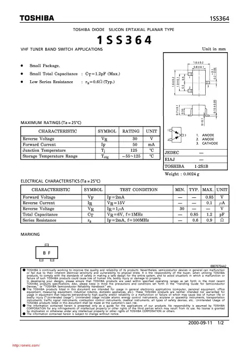
1SS364T5LFT;中文规格书,Datasheet资料
- 格式:pdf
- 大小:118.61 KB
- 文档页数:3
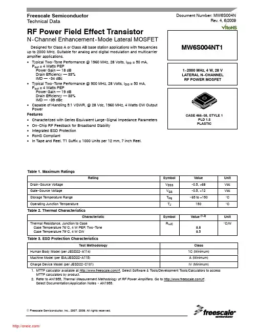
RF Power Field Effect TransistorN-Channel Enhancement-Mode Lateral MOSFETDesigned for Class A or Class AB base station applications with frequencies up to 2000 MHz. Suitable for analog and digital modulation and multicarrier amplifier applications.•Typical Two-Tone Performance @ 1960 MHz, 28 Volts, I DQ = 50 mA, P out = 4 Watts PEP Power Gain — 18 dB Drain Efficiency — 33%IMD — -34 dBc•Typical Two-Tone Performance @ 900 MHz, 28 Volts, I DQ = 50 mA, P out = 4 Watts PEP Power Gain — 19 dB Drain Efficiency — 33%IMD — -39 dBc•Capable of Handling 5:1 VSWR, @ 28 Vdc, 1960 MHz, 4 Watts CW Output Power Features•Characterized with Series Equivalent Large-Signal Impedance Parameters •On-Chip RF Feedback for Broadband Stability •Integrated ESD Protection •RoHS Compliant•In Tape and Reel. T1 Suffix = 1000 Units per 12 mm, 7 inch Reel.Table 1. Maximum RatingsRatingSymbol Value Unit Drain-Source Voltage V DSS -0.5, +68Vdc Gate-Source Voltage V GS -0.5, +12Vdc Storage Temperature Range T stg -65 to +150°C Operating Junction TemperatureT J150°CTable 2. Thermal CharacteristicsCharacteristicSymbol Value (1,2)Unit Thermal Resistance, Junction to CaseCase Temperature 76°C, 4 W PEP , Two-Tone Case Temperature 79°C, 4 W CWR θJC8.88.5°C/WTable 3. ESD Protection CharacteristicsTest MethodologyClass Human Body Model (per JESD22-A114)1C (Minimum)Machine Model (per EIA/JESD22-A115) A (Minimum)Charge Device Model (per JESD22-C101)IV (Minimum)1.MTTF calculator available at /rf. Select Software & Tools/Development Tools/Calculators to access MTTF calculators by product.2.Refer to AN1955, Thermal Measurement Methodology of RF Power Amplifiers. Go to /rf. Select Documentation/Application Notes - AN1955.Document Number: MW6S004NRev. 4, 6/2009Freescale Semiconductor Technical DataMW6S004NT1Table 4. Moisture Sensitivity LevelTest MethodologyRating Package Peak TemperatureUnit Per JESD 22-A113, IPC/JEDEC J-STD-0203260°CTable 5. Electrical Characteristics (T A = 25°C unless otherwise noted)CharacteristicSymbolMinTypMaxUnitOff CharacteristicsZero Gate Voltage Drain Leakage Current (V DS = 68 Vdc, V GS = 0 Vdc)I DSS ——10μAdc Zero Gate Voltage Drain Leakage Current (V DS = 28 Vdc, V GS = 0 Vdc)I DSS ——10μAdc Gate-Source Leakage Current (V GS = 5 Vdc, V DS = 0 Vdc)I GSS——500nAdcOn CharacteristicsGate Threshold Voltage(V DS = 10 Vdc, I D = 50 mAdc)V GS(th) 1.22 2.7Vdc Gate Quiescent Voltage(V DS = 28 Vdc, I D = 50 mAdc)V GS(Q)— 2.7—Vdc Fixture Gate Quiescent Voltage (1)(V DD = 28 Vdc, I D = 50 mAdc, Measured in Functional Test)V GG(Q) 2.23 4.2Vdc Drain-Source On-Voltage(V GS = 10 Vdc, I D = 50 mAdc)V DS(on)—0.270.37VdcDynamic CharacteristicsReverse Transfer Capacitance(V DS = 28 Vdc ± 30 mV(rms)ac @ 1 MHz, V GS = 0 Vdc)C rss —21—pF Output Capacitance(V DS = 28 Vdc ± 30 mV(rms)ac @ 1 MHz, V GS = 0 Vdc)C oss —25—pF Input Capacitance(V DS = 28 Vdc, V GS = 0 Vdc ± 30 mV(rms)ac @ 1 MHz)C iss—30—pFFunctional Tests (In Freescale Test Fixture, 50 ohm system) V DD = 28 Vdc, I DQ = 50 mA, P out = 4 W PEP , f1 = 1960 MHz, f2 = 1960.1 MHz, Two-Tone Test Power Gain G ps 16.51820dB Drain EfficiencyηD 2833—%Intermodulation Distortion IMD —-34-28dBc Input Return LossIRL—-12-10dBTypical Performance (In Freescale 900 MHz Demo Board, 50 ohm system) V DD = 28 Vdc, I DQ = 50 mA, P out = 4 W PEP , f = 900 MHz, Two-Tone Test, 100 kHz Tone Spacing Power Gain G ps —19—dB Drain EfficiencyηD —33—%Intermodulation Distortion IMD —-39—dBc Input Return LossIRL—-12—dB1.V GG = 11/10 x V GS(Q). Parameter measured on Freescale Test Fixture, due to resistive divider network on the board. Refer to Test Circuit Schematic.MW6S004NT1Figure 1. MW6S004NT1 Test Circuit SchematicZ70.210″ x 1.220″ Microstrip Z80.054″ x 0.680″ Microstrip Z90.054″ x 0.260″ Microstrip Z100.025″ x 0.930″ MicrostripPCBArlon CuClad 250GX-0300-55-22, 0.020″, εr = 2.5Z10.054″ x 0.430″ Microstrip Z20.054″ x 0.137″ Microstrip Z30.580″ x 0.420″ Microstrip Z40.580″ x 0.100″ Microstrip Z50.025″ x 0.680″ Microstrip Z60.210″ x 0.100″ MicrostripV SUPPLYTable 6. MW6S004NT1 Test Circuit Component Designations and ValuesPartDescriptionPart Number Manufacturer C1100 nF Chip Capacitor CDR33BX104AKYS Kemet C2, C3, C6, C79.1 pF Chip Capacitors ATC100B9R1CT500XT ATC C4, C510 μF, 50 V Chip Capacitors GRM55DR61H106KA88B Murata C810 μF, 35 V Tantalum Chip Capacitor T490D106K035AT Kemet R1 1 k Ω, 1/4 W Chip Resistor CRCW12061001FKEA Vishay R210 k Ω, 1/4 W Chip Resistor CRCW12061002FKEA Vishay R310 Ω, 1/4 W Chip ResistorCRCW120610R0FKEAVishayMW6S004NT1Figure 2. MW6S004NT1 Test Circuit Component LayoutMW6S004NT1TYPICAL CHARACTERISTICS1420191716G p s , P O W E R G A I N (d B )100.1TWO−TONE SPACING (MHz)1100Figure 6. Intermodulation Distortion Productsversus Tone Spacing 26P in , INPUT POWER (dBm)1618222414Figure 7. Pulsed CW Output Power versusInput PowerI M D , I N T E R M O D U L A T I O N D I S T O R T I O N (d B c )181520MW6S004NT1TYPICAL CHARACTERISTICSA C P R (dB )−70P out , OUTPUT POWER (WATTS) AVG.50−2040−3030−4020−5010−600.01110Figure 8. Single-Carrier CDMA ACPR, Power Gainand Drain Efficiency versus Output PowerP out , OUTPUT POWER (WATTS) CWFigure 10. Power Gain versus Output Power 7151906171618234G p s , P O W E R G A I N (d B )1800−250f, FREQUENCY (MHz)Figure 11. Broadband Frequency Response−5−10−15−20210020502000195019001850S 11 (d B )851ηD , D R A I N E F F I C I E N C Y (%), G p s , P O W E R G A I N (d B )0.118.517.516.515.5MW6S004NT1TYPICAL CHARACTERISTICS25010790T J , JUNCTION TEMPERATURE (°C)Figure 12. MTTF versus Junction TemperatureThis above graph displays calculated MTTF in hours when the device is operated at V DD = 28 Vdc, P out = 4 W PEP, and ηD = 33%.MTTF calculator available at /rf. Select Software & Tools/Development Tools/Calculators to access MTTF calculators by product.106105104110130150170190M T T F (H O U R S )210230MW6S004NT1f = 1930 MHzZ o = 10 ΩZ loadZ sourcef = 1990 MHzf = 1930 MHzf = 1990 MHzV DD = 28 Vdc, I DQ = 50 mA, P out = 4 W PEPfMHzZ sourceWZ loadW1930 1.96 - j5.348.78 + j6.961960 1.89 - j5.108.93 + j7.461990 1.82 - j4.859.11 + j7.97Z source=Test circuit impedance as measured fromgate to ground.Z load=Test circuit impedance as measured fromdrain to ground.Z source Z loadOutputMatchingNetworkFigure 13. Series Equivalent Source and Load ImpedanceMW6S004NT1Table 7. Common Source Scattering Parameters (V DD = 28 V, 50 ohm system)I DQ = 50 mAf MH S 11S 21S 12S 22MHz |S 11|∠φ|S 21|∠φ|S 12|∠φ|S 22|∠φ5000.649-116.3407.902105.4200.056-73.7500.548-33.5705500.695-121.6807.50298.7900.053-80.5700.593-41.4806000.733-126.5607.11192.3800.049-87.0100.632-48.8906500.770-131.340 6.69986.2900.045-93.2800.669-56.0007000.800-135.740 6.30280.4500.041-99.1200.701-62.8107500.827-140.030 5.92274.8500.038-104.8500.727-69.2908000.848-143.950 5.55269.6300.035-110.1100.750-75.3508500.866-147.690 5.22064.5800.032-115.2200.770-81.1309000.882-151.140 4.89159.9700.029-119.9600.786-86.5709500.895-154.560 4.59755.4900.026-124.7900.800-91.73010000.907-157.590 4.31551.2400.024-129.0900.813-96.66010500.916-160.540 4.06047.1700.022-133.3700.824-101.34011000.923-163.310 3.81943.3400.020-137.4600.833-105.79011500.929-165.930 3.60139.6500.018-141.4400.840-110.05012000.935-168.430 3.39836.1100.017-145.3300.847-114.17012500.938-170.770 3.21032.7400.015-149.5400.851-118.06013000.942-173.030 3.03629.4900.014-153.4300.856-121.88013500.945-175.140 2.87526.3600.013-157.4600.859-125.52014000.948-177.170 2.72823.3300.012-161.9100.863-129.02014500.951-179.090 2.59020.4400.011-166.1800.866-132.39015000.953179.030 2.46417.6400.010-170.6300.869-135.65015500.954177.270 2.34714.9200.009-174.8900.872-138.76016000.955175.570 2.24012.3200.008179.9500.875-141.75016500.956173.980 2.1399.7400.008173.9200.877-144.65017000.957172.350 2.0477.2500.007167.7100.880-147.48017500.957170.800 1.958 4.8100.007161.8100.882-150.18018000.958169.340 1.879 2.4400.006155.3700.884-152.76018500.959167.920 1.8060.2600.006148.9400.886-155.23019000.959166.510 1.736-1.9800.005142.6300.887-157.58019500.960165.200 1.668-4.3100.005136.7400.888-160.05020000.959163.800 1.611-6.2400.005129.9100.890-162.07020500.959162.420 1.555-8.2900.005123.8100.891-164.19021000.958161.170 1.504-10.2700.005118.2000.892-166.14021500.958159.840 1.456-12.2100.005112.7400.893-168.06022000.957158.560 1.412-14.1300.005108.4600.894-169.84022500.957157.160 1.372-16.0100.005103.8400.896-171.61023000.955155.870 1.334-17.8700.00599.3100.896-173.26023500.954154.510 1.300-19.7000.00595.3600.897-174.83024000.953153.120 1.268-21.5100.00591.0300.898-176.39024500.953151.7301.238-23.2500.00587.4600.899-177.840MW6S004NT1Table 7. Common Source Scattering Parameters (V DD = 28 V, 50 ohm system) (continued)I DQ = 50 mAf MH S 11S 21S 12S 22MHz |S 11|∠φ|S 21|∠φ|S 12|∠φ|S 22|∠φ25000.952150.340 1.211-25.1200.00684.1600.899-179.27025500.950149.010 1.187-26.9200.00680.7800.897179.42026000.949147.380 1.166-28.6500.00677.8800.897178.12026500.948145.920 1.144-30.4200.00774.6700.898176.84027000.944144.200 1.121-32.3100.00771.3600.896175.48027500.944142.790 1.105-34.2300.00767.9800.897174.06028000.943141.020 1.088-36.0000.00763.9500.897172.93028500.941139.410 1.073-37.8700.00761.2300.896171.63029000.940137.640 1.058-39.7600.00859.8100.896170.33029500.938135.900 1.045-41.6800.00858.2800.896169.04030000.937133.8601.032-43.6100.00856.7400.895167.510分销商库存信息: FREESCALEMW6S004NT1。

AS3604Multi-Standard Power Management Unitaustria micro systemsData Sheet1 General DescriptionThe AS3604 is a highly-integrated CMOS power manage-ment device designed specifically for portable devices such as mobile phones, PDAs, CD players, digital cam-eras and other devices powered by 1-cell lithium-based or 3- to 4-cell nickel-based batteries. It can be used for any mobile phone handset standards such as CDMA,WCDMA, GSM, GPRS, EDGE, UTMS and other Japa-nese or American standards.The device incorporates low dropout regulators (LDOs), DC/DC converters, a complete battery charger, and an audio power amplifier onto one die.The linear analog LDOs feature extremely high perfor-mance regarding:Noise – typ 30µV RMS from 100Hz to 100kHzLine/Load Regulation – < 1mV static, < 10mV transientPower Supply Rejection – > 70dB @ 1kHzThe integrated Step Down DC/DC Converter does not require an external Schottky diode yet provides very high efficiency (up to 95%) throughout the whole operating range. It can be either used as a stand-alone device or as a pre-regulator for LDOs to increase overall device effi-ciency.A Step Up DC/DC Converter is included to supply power for white LEDs, together with programmable current sources to control LED brightness.A low-distortion audio power amplifier (1 Watt @ 8Ω) sup-ports handsfree operation and HiFi ring-tones.The device also features a chemistry-independent battery charger including automatic trickle charging, gas gauge, and programmable constant voltage and current charging.The AS3604 is controlled via a serial interface and inte-grates all necessary system specific functions such as Reset, Watchdog, and Power-On Detection.Output voltages and start-up timings can be programmed on metal-mask level, by register or by an external resistor.2 Key FeaturesTen Programmable High Performance LDOs-Two Digital Low-Power LDOs (0.75 to 2.5V, 200mA; 250mA up to 1.4V)-Three RF Low-Noise LDOs (1.85 to 3.4V, 200mA) -Two RF Low-Noise LDOs (1.85 to 3.4V, 150mA; 200mA up to 2.6V)-One SIM Low-Power LDO (1.8 to 3.0V, 20mA)-One Periphery Low-Noise LDO (2.5 to 3.2V, 200mA)-One Low-Power LDO (2.5V, 10mA)Programmable High Efficiency DC/DC Converters -Step Down: 0.8 to 3.4V, up to 500mA with 2.2MHz Operating Frequency and Small External Coil (2.2µH)-Step Up: 15V, 45mA, (for White LEDs)Stereo Audio Power Amplifier-0.5W @ 4Ω – Stereo; 1W @ 8Ω – Bridged -Digital Volume Control, 3dB Steps-Click- and Pop-Less Start-Up and Power-DownComplete Chemistry-Independent Battery Charger -Integrated Gas Gauge-Automatic Trickle Charging-Programmable Constant Current Charging -Programmable Constant Voltage Charging -Pulse Charging-Safety Functions (Low Battery Shutdown)-Over- and Under-Temperature Charge Disable -Operation without Battery-Can Regulate the Current Through the Battery or from the Charger-Charger Input Overvoltage Protection (6V) -Shutdown even with Connected Charger -Charger Resume Operation-Charger Interrupts (Inserted, Removed, Overvolt-age, Resume)-No-Battery DetectionMomentary Power Loss Detection-Battery Supply Short-Interruption Detection (<200ms); (e.g., due to a dropped phone)Four Programmable Current Sources -8-Bit (0.625 to 160mA) -Buzzer -Vibrator -LEDsWide Battery Supply Range 3.0 to 5.5VFour General Purpose Switches (1Ω and 2Ω) Three Programmable General Purpose I/O Pins On-Chip Bandgap Tuning for High Accuracy (±1%) Integrated Programmable Watchdog (7.5 to 1900ms) Programmable Reset (10 to 110ms)Shutdown Current typ 7µA (2.5V Always On) Overcurrent and Thermal Protection 0.35µ CMOS Solution2.1 Watt Power Dissipation @ SCSB = 70ºC48-pin, 6x6mm QFN Package (0.4mm pitch)3 ApplicationsMulti-standard power management for mobile phones, PDAs, and any other 1-cell Li+ or 3- to 4-cell NiMh pow-ered devices.4 Block DiagramsFigure 1. AS3604 Block Diagram. Option: Audio Amplifier In Differential Mode, Step Down DC/DC Converter asPre-Regulator for Digital LDOsNote:Refer to Table 38 on page 74 for specifications of external components.2.2µHV 2_5AS3604Power ManagementUnitCharge Pump 4.74-5.25V 30mAAnalog LDO Low Noise 2.5-3.2V 200mAAnalog LDO Low Noise 1.85-3.4V 200mARF LDO Low Noise 1.85-3.4V 200mARF LDO Low Noise 1.85-3.4V 200mA RF LDO Low Noise 1.85-3.4V 200mARF LDO Low Noise 1.85-3.4V 200mAStep Up DC/DC Converter ≤15V 45mACurrent Source 4x(0.6-160mA)L122µHV BATCAPP CAPN 32C2330nFV 5_6Charge PumpC31µFC41µFC61µFC81µFC91µF C131µFBaseband Analog3.0-5.5V Baseband CoreRFTransmitterRFReceiver3.0-5.5VV BATVCO TXCOSynthesizer etc.Internal LDO 2.5V, 10mAC51µF C722µFC101µFC121µF V 2_5ON SwitchInterrupt, LCD Control, etc.Digital LDO 0.75-2.5V 250mA SIM LDO 3.0V, 20mAC111µFDigital LDO 0.75-2.5V 250mAStep Down DC/DCConverter 1.0-3.0V, 500mAC141µFC151µFFlash Memory BasebandCore (Alternate)LX 48C161µFC1810µFBaseband PeripheralsC19100nFSIM CardPORV ANA_1Digital Logic and ReferencesBoot ROMR7R PROGRAMR6220k ΩC29100nF242623RPROGRAMCREF RBIAS 10RESETR5100k ΩRESETV ANA_1I/FSerial InterfaceV 2_5 or V BAT NiMh, LiIonBattery Charger andGas GaugeR34.7k ΩR24.7k ΩC27R450m ΩC281µFLi-Ion NiMhV BATAll caps on V BAT≥10µF totalPadGND_PADC261µF R12k ΩDC Char-ger Adapter ≤15V≥8ΩLS11W Audio AmplifierC23100nF C24100nF AudioInC25100nFV BATC221µFC11µFSTEPUP36D1MBR0520White LEDs VibratorBuzzer CURR135343332CURR2CURR3CURR4VSIM46FeedbackQ1Si3441V BAT 3.0-5.5VL2VBAT_247VBUCK 40VDIG_239VDIG_141V2_522VRF_419VBAT_518VRF_317VRF_27VBAT_48VRF_19VANA_26VBAT_15VANA_14V5_61VBAT_330AOUT_L 28AIN_L 38AGND 31AIN_R 37AOUT_R29VCHARGER20VGATE21ISENSP15ISENSN 16GND_SENSE27ON 25SDI12SCLK 13SDO 11SCSB14GPIOV ANA_1 V 5_6GPIO343GPIO244GPIO145VBAT_642V BAT 3.0-5.5VFigure 2. AS3604 Block Diagram. Option: Audio Amplifier in Stereo Single-Ended Mode, Digital LDOs Separatedfrom Step Down DC/DC ConverterNote:Refer to Table 38 on page 74 for specifications of external components.NiMh, LiIonBattery Charger andFuel GaugeAS3604Power ManagementUnitCharge Pump 4.74-5.25V 30mAAnalog LDO Low Noise 2.5-3.2V 200mAAnalog LDO Low Noise 1.85-3.4V 200mARF LDO Low Noise 1.85-3.4V 200mARF LDO Low Noise 1.85-3.4V 200mA RF LDO Low Noise 1.85-3.4V 200mARF LDO Low Noise 1.85-3.4V 200mAStep Up DC/DC Converter ≤15V 45mACurrent Source 4x(0.6-160mA)L122µHV BATCAPP CAPN 32C2330nFV 5_6Charge PumpC31µFBaseband Analog3.0-5.5V Baseband CoreRFTransmitterRFReceiverGPIO3.0-5.5VV BATVCO TXCOSynthesizer etc.Internal LDO2.5V 10mAV 2_5ON SwitchInterrupt, LCD Control, etc.V ANA_1 V 5_6Digital LDO 0.75-2.5V 250mA SIM LDO 3.0V, 20mADigital LDO 0.75-2.5V 250mAStep Down DC/DCConverter 1.0-3.0V, 500mAFlash Memory 3.0-5.5VSIM CardPORV ANA_1Digital Logic and ReferencesBoot ROM10RESETR5100k ΩRESETV ANA_1I/FSerial InterfaceV 2_5 or V BATR34.7k ΩR24.7k ΩC27R450m ΩC281µFLi-Ion NiMhV BATAll caps on V BAT≥10µF totalC261µF R12k ΩDC Char-ger Adapter ≤15V≥4ΩLS21W Audio AmplifierC20≥100µF C21≥100µFIN _LV BATC221µFC11µFSTEPUP36D1MBR0520White LEDs Vibrator Buzzer CURR135343332CURR2CURR3CURR4V 2_51.0-5.5V FeedbackQ1Si3441≥4ΩLS3IN _RC23100nFC25100nF Baseband Core(Alternative)C24100nFR7R PROGRAMR6220k ΩC29100nF242623RPROGRAM CREF RBIASPadGND_PADC41µFC51µF C101µFC91µF C111µFC121µF C131µFC19100nFC301µFC722µFC141µFVBAT_330AOUT_L28AIN_L 38AGND 31AIN_R37AOUT_R29VCHARGER20VGATE21ISENSP15ISENSN 16GND_SENSE27ON 25SDI12SCLK 13SDO 11SCSB14LX 48VSIM46VBAT_247VBUCK 40VDIG_239VDIG_141GPIO343GPIO244GPIO145V2_522VRF_419VBAT_518VRF_317VRF_27VBAT_48VRF_19VANA_26VBAT_15VANA_14V5_61C61µFC81µFC151µFVBAT_642V BAT 3.0-5.5V2.2µHC161µFC1810µF Baseband PeripheralsL2Content1 General Description (1)2 Key Features (1)3 Applications (1)4 Block Diagrams (2)5 Absolute Maximum Ratings (Non-Operating) (6)5.1 Operating Conditions (6)6 Detailed Functional Descriptions (7)6.1 Battery Charger Controller (7)6.2 Step Down DC/DC Converter (24)6.3 Low Dropout Regulators (30)6.4 Charge Pump (41)6.5 Step Up DC/DC Converter (42)6.6 General Purpose Input/Output (44)6.7 Current Sinks (50)6.8 Audio Amplifier (53)7 System Supervisory Functions (56)7.1 Reset (56)7.2 Startup (58)7.3 Protection Functions (59)7.4 Watchdog Block (60)7.5 Internal Reference Circuits (61)7.6 Low Power Mode (63)7.7 Boot Sequence Detection (63)7.8 Serial Interface (64)8 Register Map (68)9 Pinout and Packaging (70)9.1 Pin Descriptions (70)9.2 Package Drawings and Markings (72)10 External Parts List (74)11 Ordering Information (75)Revision HistoryRevision Date Owner Description1.023 June 2006ptr - Initial release.1.1 3 March 2007ptr- Updated ambient temperature range.1.11 4 Dec 2008pkm- Updated internal LDO supply description1.28 Apr 2009pkm- Updated ordering info for AS3604B chip version1.2115 Mai 2009pkm - Updated abs. max ratings and stand-by current, deleted errata1.2221 Aug 2009pkm- Updated operating current, SNR and VCHOV5 Absolute Maximum Ratings (Non-Operating)Stresses beyond the absolute maximum ratings may cause permanent damage to the AS3604. These are stress rat-ings only. Functional operation of the device at these or beyond those in Operating Conditions is not implied. Caution:Exposure to absolute maximum rating conditions may affect device reliability.5.1 Operating ConditionsTable 1. Absolute Maximum Ratings Symbol Parameter Min Max Unit NotesV IN_HVHigh Voltage Pins-0.318.0VApplicable for high voltage pins: VCHARGER, VGATE, and STEPUP V IN_MV 5V Pins -0.37.0VApplicable for pins 5V pins:VBAT_1 - VBAT_6, V5_6, VBUCK, GPIO1 - GPIO3, CURR1 - CURR4, AIN_L, AIN_R, AOUT_L, AOUT_R, VRF_1 - VRF_4 (when not in LDO-mode), ON, and LXV IN_LV 3.3V Pins -0.3 5.0VApplicable for 3.3V pins:RESET, SCSB, SCLK, SDI, SDO, VANA_1, VANA_2, VSIM, VDIG_1, VDIG_2, CAPN, AGND, ISENSP, ISENSN, V2_5, CREF, RBIAS, and RPROGRAM I IN Input Pin Current -25+25mA At 25ºC Norm: JEDEC 17T strg Storage Temperature Range-55125ºC Humidity585%Non-condensingV ESD Electrostatic Discharge -10001000V Norm: MIL 883 E Method 3015; ±1000V.P T Total Power Dissipation 2.1W T AMB = 70ºCT maxPeak Reflow SolderingTemperature260ºCT = 20 to 40s, according to the IPC/JEDEC J-STD 020C.Table 2. Operating Conditions Symbol Parameter Min TypMax Unit NotesV HV High Voltage 0.015.0V Pins VCHARGER, VGATE and STEPUP V BAT Battery Voltage 3.0 3.6 5.5V For pins VBAT_1 - VBAT_6. Duringstartup from ext. battery charger adapter, the battery voltage can be below 3.0V.V ANA_1Periphery Supply Voltage (for RESET and SPI pins) 2.5Boot ROM 3.2V Internally generated from V ANA_1.V ON Activation voltage for ON pin1.75V 2_5V BAT V V 2_5Voltage on Pin V2_52.4 2.5 2.6V Internally generated.V 5_6Output Voltage of Charge Pump5.0 5.2 5.6V 2 x V ANA_1T AMB Ambient Temperature -402585ºC I BATOperating Current 195260µANormal operating current. With bitlow_power_on (page 62) = 0; only V ANA_1 active, no additional external loads.I LOWPOWER Low-Power Mode CurrentConsumption 110µAWith bit low_power_on (page 62) = 1; only V ANA_1 active, no additional external loads.I POWEROFF Power-Off Mode CurrentConsumption1320µAWith bit power_off (page 57) = 1; only V2_5 is active in power off mode.not tested, guaranteed by design6 Detailed Functional Descriptions6.1 Battery Charger ControllerThe AS3604 can serve as a standalone Battery Charger Controller supporting rechargeable lithium-ion (Li+), lithium-polymer (LiPo) and 3- or 4-cell nickel metal-hydride (NiMh) batteries.The main features of the Battery Charger Controller are:Constant Voltage Charge Mode – Described on page 9 Pulse Charge Mode – Described on page 11Battery Presence Detection – Described on page 14 Operation Without Battery – Described on page 14 Charge Controller Bypass – Described on page 14Overvoltage and Undervoltage Supervision – Described on page 15Figure 3. Battery Charger Controller Block DiagramTable 3. Battery Charger Controller ComponentsSymbol Parameter ValueNotesM CHG P-Channel MOSFET Si3441BDV, Si8401DB or similar The maximum power dissipation of thistransistor is not limited by the AS3604.R PUP Pull-Up Resistor 2K Ω ± 5%R SENSE Current Sense Resistor50m Ω ± 1%, 125mW for I VBAT,DC < 1.5Ae.g. Vishay Dale WSL0805R FILT1,2Filter Resistor 47K Ω ± 1%Can be omitted if Gas Gauge functionalityis not used (R FILT1,2 = 0Ω)C FILT Filter Capacitor 100nF ± 20%, X5R or X7R Dielectric C CHRG Bypass Capacitor on pin VCHARGER 1µF ± 20%, X5R or X7R DielectricC BATMinimum Total CapacitanceParallel to Battery10µF C BATVCHARGERR SENSE AS3604Battery Charger ControllerVGATEVBAT_5ISENSPISENSNVSSR PUPM CHGR FILT1BATTGND_PCBV BATChargerC CHRGC FILTR FILT26.1.1 Low-Current Trickle Charge ModeLow-Current Trickle Charge mode is initiated when an external battery charger has been detected, bit chDet (page 19)= 1, and the battery voltage is below the VUVLO threshold; bits ChAct (page 19) and Trickle (page 19) will be set. In Trickle Charge mode the charge current will be limited to the value specified by Trickle Current (page 21) to prevent undue stress on either the battery or the Battery Charger in case of deeply discharged batteries.Once VUVLO has been exceeded, the Battery Charger will terminate Trickle Charge mode (charger must not be dis-abled between trickle and constant current (fast) charging), reset bits ChAct and Trickle , and switch on the device.The trickle charge is terminated in any case after approximately 60 minutes (as it is assumed that the battery is dam-aged in this case)6.1.2 Constant Current Charge ModeConstant Current mode is initiated by setting bit ChEn (page 20) and resetting bit Fast (page 20). Bit ChAct (page 19) is set automatically when the Battery Charger starts. Charge current will be limited to the value specified by bit Constant Current (page 21) by the Battery Charger Controller.6.1.3 Charging Nickel-based BatteriesFor nickel-based batteries (NiMh), BatType (page 20) must be 1 (see Figure 4 on page 9). The endpoint detection (ΔV/Δt) must be performed by the host controller. It must turn off the charger duly to avoid overcharging. In any case, when the battery voltage exceeds the charge termination threshold (typ. 5.5V), the charger will be turned off and bit EOC (page 20) will be set.6.1.4 Charging Lithium-based BatteriesFor lithium-based batteries (Lithium-Ion, Lithium-Polymer), BatType (page 20) must be 0. Additionally, bit Li4v2(page 20) can select between coke- and graphite-anode, setting different charge termination thresholds (typ. 4.1 or 4.2V). The charger is designed to charge 1-cell lithium-based batteries independently, using Trickle Charge, Constant Current, Constant Voltage, or Pulse Charge modes.When the battery voltage exceeds the charge termination threshold during Constant Current mode, it automatically continues charging with either Constant Voltage mode, bit Pulse (page 20), or Pulse Charge mode, Pulse , and termi-nates when the end-of-charge conditions are met (see Figure 5 on page 11 and Figure 6 on page 13).Table 4. Battery Charger Controller Parameters Symbol ParameterMin Typ Max Unit NotesV CHDET Charger Detection Threshold. VCHARGER - VBAT_5: Charger On 5075105mV Hysteresis = (V CHDET - V CHMIN )< 40mVV CHMIN Charger Detection Threshold. VCHARGER - VBAT_5: Charger Off52035mV V CHREG Bootstrap Regulator Voltage 2.4 2.52.6V VCHARGER > 5VV CHOVH VCHARGER Overvoltage Detection6.26.456,71VMonitor voltage on VCHARGER and disable charging if this voltage is exceeded.V CHOV 5,81 6.056,29V UVLO Undervoltage Lockout Threshold 3.1V V BAT rising 2.8V BAT falling V OVLOOvervoltage Lockout Threshold5.5VV BAT rising 5.4V BAT fallingV CHOFF Charge Termination Threshold4.14 4.20 4.26VLi+ Battery: BatType (page 20) = 0, Li4v2(page 20) = 14.05 4.1 4.15Li+ Battery: BatType = 0, Li4v2 = 0.From -5 to +50ºC 5.445.55.6NiMh Battery: BatType = 1V NOBATDET No-Battery Detection Threshold andCharger Resume Detection Threshold3.644VDisOWB (page 21) = 0Figure 4. Startup and Constant Current Charging of Nickel-based Batteries6.1.5 Fast Charge ModeAs an alternative to Constant Current mode, Fast Charge mode may be selected. The charge current will not be con-trolled in this mode and is only limited by the external battery charger adapter.Fast Charge mode is initiated by setting bits ChEn (page 20) and Fast (page 20). Bit ChAct (page 19) is set when the Bat-tery Charger has started.End of ChargeIn Fast Charge mode, the same charge termination thresholds apply as for Constant Current mode. Additionally,depending on bit Fast (page 20), the current during pulse charging is either the selected constant current or maximum. Charging will resume if the battery voltage drops below V NOBATDET .6.1.6 Constant Voltage Charge ModeConstant Voltage mode is initiated and bit CVM (page 19) will be set when threshold V CHOFF (page 8) has been exceeded for the first time (no debounce filter) and bit Pulse (page 20) is not set.External Charger at Pin V CHARGERPrinciple Only. Not To Scale.V BATI CHARGETrickle CurrentConstant Current or Fast CurrentV UVLO 3.1VV CHDET0VPower up LDOs = Boot ROMLDO Voltages Serial Communication PossibleResetRegister Settings (Write)ChEn µC: ActivateCharger μC: Turn Off ChargerPulseChDet Register Settings (Read)Trickle ChAct CVM EOCTrickle Charge ModePower Up; No ChargeConstant Current ModeBit EOC is only set when V CHOFF is exceededt = 06-11mst10-110msΔV/ΔI Detection by External ADCV CHOFF = 5.5V (BatType = 1)CC Charging Terminates Immediately when V CHOFF is exceeded BatType µC: Select Battery TypeThe charge controller will regulate the battery voltage to a value set by bit Li4v2(page 20). To enable operation of the device without a battery connected to the system it is necessary that the charger is not disabled between the moment when the V CHOFF threshold is exceeded for the first time and the beginning of constant voltage charge mode.During Constant Voltage mode, the charge current will decrease and eventually drop below the value set by Trickle Current(page 21). If the measured charge current is less than or equal to Trickle Current, charging is terminated and bit EOC is set. Charging will resume if the battery voltage drops below V NOBATDET.If the battery has been removed during constant voltage charging the EOC condition and the no battery condition will probably conflict. To be able to properly detect the EOC state the EOC condition has to be dominant over the no battery condition.If the battery voltage (VBAT_5) drops below V NOBATDETECT (page 8) (signal resume starts pulsing), e.g. if the bat-tery is removed after charging is finished, EOC(page 20) will be cleared (after debounce time) and the battery char-ger controller will resume in constant voltage mode to enable operation of the device without battery. This only works if bit CVM(page 19) remains set when bit EOC is set, otherwise the comparators that are required for operation without battery are gated.Three scenarios are possible at this point:1. If a battery is connected the charge current will now be high and charging will return to constant current charg-ing.2. No battery is connected and no current will flow through the sense resistor. Now the no battery condition isdetected properly.3. The battery was connected and is disconnected. No current will flow through the sense resistor and the no bat-tery condition is detected properly.In summary: When charging is resumed after an EOC state either a (dis)charge current will be measured and the charge controller will return to constant current mode or no current will be measured and a “no battery”condition is indicated. To be able to handle supply voltage spikes caused by e.g. battery bouncing when the system is heavily shaken the V NOBATDETECT detection has to be debounced for 1 current measurement cycle before EOC is cleared. After the debounce time is over additional pulses must occur during the next current measurement cycle to clear EOC.The no battery status is indicated with bit NoBat(page 20).If the battery is replaced after charging is finished and the charge current exceeds the value set by ConstantCurrent(page 21), the charge controller will clear bit CVM and return to Constant Current or Fast Charge mode, depend-ing on bit Fast(page 20).Notes:1. Bit CVM will be ambiguous if bit Fast is set.2. EOC will only be entered if bit AutoChgTerm(page 21) is set (default = 0).分销商库存信息:AMSAS3604-ZQFT AS3604-ZQFU。
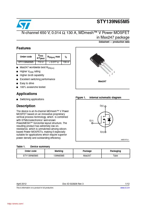
This is information on a product in full production.April 2012Doc ID 022826 Rev 31/12STY139N65M5N-channel 650 V , 0.014 Ω, 130 A, MDmesh™ V Power MOSFETin Max247 packageDatasheet — production dataFeatures■Max247 worldwide best R DS(on)■Higher V DSS rating ■Higher dv/dt capability■Excellent switching performance ■Easy to drive■100% avalanche testedApplications■Switching applicationsDescriptionThe device is an N-channel MDmesh™ V Power MOSFET based on an innovative proprietary vertical process technology, which is combined with STMicroelectronics’ well-knownPowerMESH™ horizontal layout structure. The resulting product has extremely low on-resistance, which is unmatched among silicon-based Power MOSFETs, making it especially suitable for applications which require superior power density and outstanding efficiency.Order code V DSS @T jMAX R DS(on) max I D STY139N65M5710 V< 0.017 Ω130 ATable 1.Device summaryOrder code Marking Package Packaging STY139N65M5139N65M5Max247TubeContents STY139N65M5Contents1Electrical ratings . . . . . . . . . . . . . . . . . . . . . . . . . . . . . . . . . . . . . . . . . . . . 32Electrical characteristics . . . . . . . . . . . . . . . . . . . . . . . . . . . . . . . . . . . . . 42.1Electrical characteristics (curves) . . . . . . . . . . . . . . . . . . . . . . . . . . . . 6 3Test circuits . . . . . . . . . . . . . . . . . . . . . . . . . . . . . . . . . . . . . . . . . . . . . . 8 4Package mechanical data . . . . . . . . . . . . . . . . . . . . . . . . . . . . . . . . . . . . . 9 5Revision history . . . . . . . . . . . . . . . . . . . . . . . . . . . . . . . . . . . . . . . . . . . 122/12Doc ID 022826 Rev 3STY139N65M5Electrical ratingsDoc ID 022826 Rev 33/121 Electrical ratingsTable 2.Absolute maximum ratingsSymbol ParameterValue Unit V GS Gate- source voltage± 25V I D Drain current (continuous) at T C = 25 °C 130A I D Drain current (continuous) at T C = 100 °C 78A I DM (1)1.Pulse width limited by safe operating area.Drain current (pulsed)520A P TOT Total dissipation at T C = 25 °C625W I AR Max current during repetitive or single pulse avalanche(pulse width limited by T JMAX )15A E AS Single pulse avalanche energy(starting T j = 25°C, I D = I AR , V DD = 50V)2000mJ dv/dt (2)2.I SD ≤ 130 A, di/dt = 400 A/µs, V DD = 400 V, peak V DS < V (BR)DSS.Peak diode recovery voltage slope 15V/ns T stg Storage temperature- 55 to 150°C T jMax. operating junction temperature150°CTable 3.Thermal dataSymbolParameterValue Unit R thj-case Thermal resistance junction-case max 0.2°C/W R thj-amb Thermal resistance junction-ambient max 30°C/W T lMaximum lead temperature for soldering purpose300°CElectrical characteristics STY139N65M54/12Doc ID 022826 Rev 32 Electrical characteristics(T C = 25 °C unless otherwise specified)Table 4.On /off statesSymbol Parameter Test conditionsMin.Typ.Max.Unit V (BR)DSS Drain-sourcebreakdown voltageI D = 1 mA, V GS = 0650V I DSS Zero gate voltage drain current (V GS = 0)V DS = 650 VV DS = 650 V , T C =125 °C 10100µA µA I GSS Gate-body leakage current (V DS = 0)V GS = ± 25 V±100nA V GS(th)Gate threshold voltage V DS = V GS , I D = 250 µA 345V R DS(on)Static drain-source onresistanceV GS = 10 V , I D = 65 A0.0140.017ΩTable 5.DynamicSymbol Parameter Test conditionsMin.Typ.Max.Unit C iss C oss C rss Input capacitance Output capacitance Reverse transfer capacitance V DS = 100 V , f = 1 MHz, V GS = 0-156003659-pF pF pFC o(tr)(1)1.C o(tr) is a constant capacitance value that gives the same charging time as C oss while V DS is rising from 0to 80% V DSS .Equivalentcapacitance time relatedV GS = 0, V DS = 0 to 520 V-1559-pFC o(er)(2)2.C o(er) is a constant capacitance value that gives the same stored energy as C oss while V DS is rising from 0to 80% V DSS .Equivalentcapacitance energy related V GS = 0, V DS = 0 to 520 V -360-pFR GIntrinsic gate resistancef = 1 MHz open drain - 1.2-ΩQg Q gs Q gdT otal gate charge Gate-source charge Gate-drain chargeV DD = 520 V , I D = 65 A,V GS = 10 V (see Figure 15)-36388164-nC nC nCSTY139N65M5Electrical characteristicsDoc ID 022826 Rev 35/12Table 6.Switching timesSymbol ParameterTest conditions Min.Typ.Max.Unitt d(v)t r(v)t f(i)t c(off)Voltage delay time Voltage rise time Current fall time Crossing timeV DD = 400 V , I D = 80 A, R G = 4.7 Ω, V GS = 10 V (see Figure 16)(see Figure 19)-295563784-ns ns ns nsTable 7.Source drain diodeSymbol ParameterTest conditionsMin.Typ.Max.Unit I SD I SDM (1)1.Pulse width limited by safe operating area.Source-drain currentSource-drain current (pulsed)-130520A A V SD (2)2.Pulsed: pulse duration = 300 µs, duty cycle 1.5%Forward on voltage I SD = 130 A, V GS = 0- 1.5V t rr Q rr I RRM Reverse recovery time Reverse recovery charge Reverse recovery current I SD = 130 A, di/dt = 100 A/µs V DD = 100 V (see Figure 16)-5701553ns µC A t rr Q rr I RRMReverse recovery time Reverse recovery charge Reverse recovery currentI SD = 130 A, di/dt = 100 A/µs V DD = 100 V , T j = 150 °C (see Figure 16)-7202468ns µC AElectrical characteristics STY139N65M5 2.1 Electrical characteristics (curves)6/12Doc ID 022826 Rev 3STY139N65M5Electrical characteristicsDoc ID 022826 Rev 37/12Figure 10.Normalized gate threshold voltageFigure 11.Normalized on resistance vsFigure 12.Output capacitance stored energyFigure 13.Switching losses vs gate resistance(1)1.Eon including reverse recovery of a SiC diode.Test circuits STY139N65M58/12Doc ID 022826 Rev 33 Test circuitsFigure 14.Switching times test circuit forFigure 15.Gate charge test circuitFigure 16.Test circuit for inductive loadFigure 17.Unclamped inductive load testFigure 18.Unclamped inductive waveformFigure 19.Switching time waveformSTY139N65M5Package mechanical data 4 Package mechanical dataIn order to meet environmental requirements, ST offers these devices in different grades ofECOP ACK® packages, depending on their level of environmental compliance. ECOPACK®specifications, grade definitions and product status are available at: .ECOP ACK® is an ST trademark.Table 8.Max247 mechanical datammDim.Min.Typ.Max.A 4.70 5.30A1 2.20 2.60b 1.00 1.40b1 2.00 2.40b2 3.00 3.40c0.400.80D19.7020.30e 5.35 5.55E15.3015.90L14.2015.20L1 3.70 4.30Doc ID 022826 Rev 39/12Package mechanical data STY139N65M510/12Doc ID 022826 Rev 3分销商库存信息: STMSTY139N65M5。
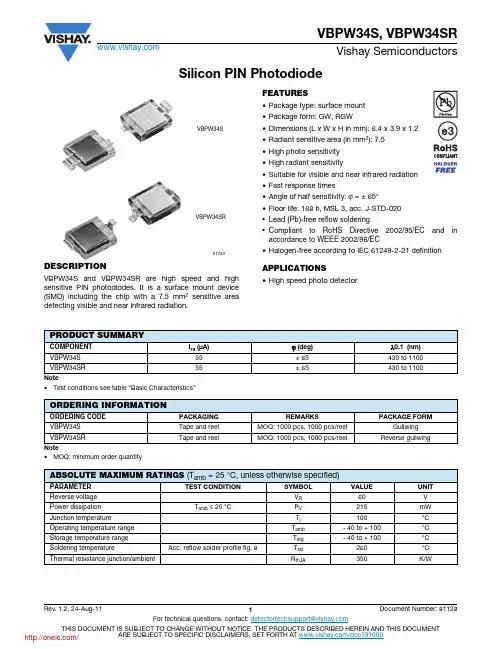
Silicon PIN PhotodiodeDESCRIPTIONVBPW34S and VBPW34SR are high speed and high sensitive PIN photodiodes. It is a surface mount device (SMD) including the chip with a 7.5 mm2 sensitive area detecting visible and near infrared radiation.FEATURES•Package type: surface mount•Package form: GW, RGW•Dimensions (L x W x H in mm): 6.4 x 3.9 x 1.2•Radiant sensitive area (in mm2): 7.5•High photo sensitivity•High radiant sensitivity•Suitable for visible and near infrared radiation•Fast response times•Angle of half sensitivity: ϕ = ± 65°•Floor life: 168 h, MSL 3, acc. J-STD-020•Lead (Pb)-free reflow soldering•Compliant to R oHS Directive 2002/95/EC and in accordance to WEEE 2002/96/EC•Halogen-free according to IEC 61249-2-21 definition APPLICATIONS•High speed photo detectorNote•Test conditions see table “Basic Characteristics”Note•MOQ: minimum order quantity21733 VBP W34SVBP W34SRPRODUCT SUMMARYCOMPONENT I ra (μA)ϕ (deg)λ0.1 (nm)V BPW34S55± 65430 to 1100V BPW34SR55± 65430 to 1100ORDERING INFORMATIONORDERING CODE PACKAGING REMARKS PACKAGE FORM V BPW34S Tape and reel MOQ: 1000 pcs, 1000 pcs/reel GullwingV BPW34SR Tape and reel MOQ: 1000 pcs, 1000 pcs/reel Reverse gullwing ABSOLUTE MAXIMUM RATINGS (T amb = 25 °C, unless otherwise specified)PARAMETER TEST CONDITION SYMBOL VALUE UNIT Reverse voltage V R60V Power dissipation T amb≤ 25 °C P V215mW Junction temperature T j100°C Operating temperature range T amb- 40 to + 100°C Storage temperature range T stg- 40 to + 100°C Soldering temperature Acc. reflow solder profile fig. 8T sd260°C Thermal resistance junction/ambient R thJA350K/WBASIC CHARACTERISTICS (T amb = 25 °C, unless otherwise specified)Fig. 1 - Reverse Dark Current vs. Ambient Temperature Fig. 2 - Relative Reverse Light Current vs. Ambient TemperatureBASIC CHARACTERISTICS (T amb = 25 °C, unless otherwise specified)PARAMETER TEST CONDITIONSYMBOLMIN.TYP.MAX.UNIT Forward voltage I F = 50 mA V F 11.3V Breakdown voltage I R = 100 μA, E = 0V (BR)60VReverse dark current V R = 10 V, E = 0I ro 230nA Diode capacitance V R = 0 V, f = 1 MHz, E = 0C D 70pF V R = 3 V, f = 1 MHz, E = 0C D 2540pF Open circuit voltageE e = 1 mW/cm 2, λ = 950 nm V o 350mV Temperature coefficient of V o E e = 1 mW/cm 2, λ = 950 nm TK Vo - 2.6mV/K Short circuit currentE e = 1 mW/cm 2, λ = 950 nm I k 50μA Temperature coefficient of I k E e = 1 mW/cm 2,λ = 950 nm TK Ik 0.1%/K Reverse light current E e = 1 mW/cm 2, λ = 950 nm,V R = 5 VI ra 4555μA Angle of half sensitivity ϕ± 65deg Wavelength of peak sensitivity λp 940nm Range of spectral bandwidth λ0.1430 to 1100nm Noise equivalent power V R = 10 V, λ = 950 nm NEP 4 x 10-14W/√Hz Rise time V R = 10 V, R L = 1 k Ω,λ = 820 nm t r 100ns Fall timeV R = 10 V, R L = 1 k Ω,λ = 820 nmt f100nsFig. 3 - Reverse Light Current vs. IrradianceFig. 4 - Reverse Light Current vs. Reverse Voltage Fig. 5 - Diode Capacitance vs. Reverse VoltageFig. 6 - Relative Spectral Sensitivity vs. WavelengthFig. 7 - Relative Radiant Sensitivity vs. Angular DisplacementPACKAGE DIMENSIONS FOR VBPW34S in millimetersPACKAGE DIMENSIONS FOR VBPW34SR in millimetersTAPING DIMENSIONS FOR VBPW34S in millimetersTAPING DIMENSIONS FOR VBPW34SRin millimetersREEL DIMENSIONS FOR VBPW34S AND VBPW34SR in millimeters SOLDER PROFILEFig. 8 - Lead (Pb)-free Reflow Solder Profileacc. J-STD-020DRYPACKDevices are packed in moisture barrier bags (MBB) to prevent the products from moisture absorption during transportation and storage. Each bag contains a desiccant. FLOOR LIFETime between soldering and removing from MBB must not exceed the time indicated in J-STD-020:Moisture sensitivity: level 3Floor life: 168 hConditions: T amb < 30 °C, RH < 60 %DRYINGIn case of moisture absorption devices should be baked before soldering. Conditions see J-STD-020 or recommended conditions:192 h at 40 °C (+ 5 °C), RH < 5 %or96 h at 60 °C (+ 5 °C), RH < 5 %.Legal Disclaimer Notice VishayDisclaimerALL PRODU CT, PRODU CT SPECIFICATIONS AND DATA ARE SU BJECT TO CHANGE WITHOU T NOTICE TO IMPROVE RELIABILITY, FUNCTION OR DESIGN OR OTHERWISE.Vishay Intertechnology, Inc., its affiliates, agents, and employees, and all persons acting on its or their behalf (collectively,“Vishay”), disclaim any and all liability for any errors, inaccuracies or incompleteness contained in any datasheet or in any other disclosure relating to any product.Vishay makes no warranty, representation or guarantee regarding the suitability of the products for any particular purpose or the continuing production of any product. To the maximum extent permitted by applicable law, Vishay disclaims (i) any and all liability arising out of the application or use of any product, (ii) any and all liability, including without limitation special, consequential or incidental damages, and (iii) any and all implied warranties, including warranties of fitness for particular purpose, non-infringement and merchantability.Statements regarding the suitability of products for certain types of applications are based on Vishay’s knowledge of typical requirements that are often placed on Vishay products in generic applications. Such statements are not binding statements about the suitability of products for a particular application. It is the customer’s responsibility to validate that a particular product with the properties described in the product specification is suitable for use in a particular application. Parameters provided in datasheets and/or specifications may vary in different applications and performance may vary over time. All operating parameters, including typical parameters, must be validated for each customer application by the customer’s technical experts. Product specifications do not expand or otherwise modify Vishay’s terms and conditions of purchase, including but not limited to the warranty expressed therein.Except as expressly indicated in writing, Vishay products are not designed for use in medical, life-saving, or life-sustaining applications or for any other application in which the failure of the Vishay product could result in personal injury or death. Customers using or selling Vishay products not expressly indicated for use in such applications do so at their own risk and agree to fully indemnify and hold Vishay and its distributors harmless from and against any and all claims, liabilities, expenses and damages arising or resulting in connection with such use or sale, including attorneys fees, even if such claim alleges that Vishay or its distributor was negligent regarding the design or manufacture of the part. Please contact authorized Vishay personnel to obtain written terms and conditions regarding products designed for such applications.No license, express or implied, by estoppel or otherwise, to any intellectual property rights is granted by this document or by any conduct of Vishay. Product names and markings noted herein may be trademarks of their respective owners.Material Category PolicyVishay Intertechnology, Inc. hereb y certifies that all its products that are identified as RoHS-Compliant fulfill the definitions and restrictions defined under Directive 2011/65/EU of The European Parliament and of the Council of June 8, 2011 on the restriction of the use of certain hazardous substances in electrical and electronic equipment (EEE) - recast, unless otherwise specified as non-compliant.Please note that some Vishay documentation may still make reference to RoHS Directive 2002/95/EC. We confirm that all the products identified as being compliant to Directive 2002/95/EC conform to Directive 2011/65/EU.分销商库存信息:VISHAYVBPW34S VBPW34SR。