南京优倍隔离器说明书
- 格式:pdf
- 大小:208.92 KB
- 文档页数:2
关于优倍安全栅国家标准主编单位中石化安全栅框架协议单位工信部两化融合贯标单位工信部智能工厂标准化示范验证单位江苏省电涌保护器工程技术研究中心南京优倍电气有限公司成立于2002年,江苏省高新技术企业。
公司致力于安全栅、隔离器、温度变送器、电涌保护器、安全继电器等工业信号接口仪表的研发制造,并为以上产品国标组组长单位,主持起草《隔离式安全栅》等国家标准。
优倍电气是国内该专业市场的主要供应商之一,品牌及品质享受盛誉。
公司为工信部两化融合体系贯标试点单位、工信部智能工厂标准化示范验证单位、江苏省、南京市首批示范智能工厂。
先后被江苏省省委、省政府授予百家江苏省优秀企业、江苏制造突出贡献奖优秀企业、江苏科技小巨人企业等光荣称号。
公司总部及新建并投产运营的优倍智造园均位于南京江宁经济技术开发区,占地面积30亩,全公司现有员工160余名,建有江苏省研究生工作站、江苏省电涌保护器工程技术研究中心、南京市工程应用研究中心,在工业测控领域有着深厚的科研基础及广泛的应用经验,产品获得多项国内、国际认证。
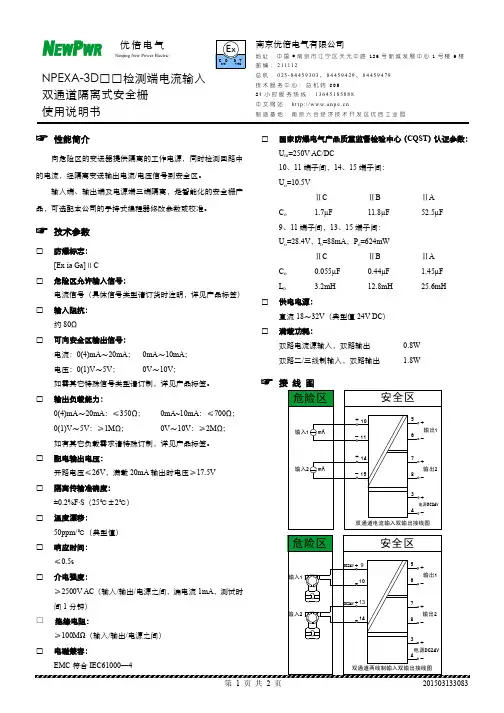
SILIEC 61508目录G系列隔离式安全栅(端子供电)通用型温度变送(常用产品型号)NPEXA-G01 (单通道,1路4 ~ 20mA输出,智能型)NPEXA-G011 (单通道,2路4 ~ 20mA输出,智能型)NPEXA-G0D11 (双通道,2路有源/无源4 ~ 20mA输出,智能型)热电偶输入(常用产品型号)NPEXA-G11 (单通道,1路4 ~ 20mA输出,智能型)NPEXA-G111 (单通道,2路4 ~ 20mA输出,智能型)NPEXA-G1D11 (双通道,2路有源/无源4 ~ 20mA输出,智能型)NPEXA-G11L (单通道,1路4 ~ 20mA输出,回路供电,智能型)热电阻输入(常用产品型号)NPEXA-G21 (单通道,1路4 ~ 20mA输出,智能型)NPEXA-G211 (单通道,2路4 ~ 20mA输出,智能型)NPEXA-G2D11 (双通道,2路有源/无源4 ~ 20mA输出,智能型)NPEXA-G27 (单通道,1路1:1电阻输出,智能型)NPEXA-G277 (单通道,2路1:1电阻输出,智能型)NPEXA-G21L (单通道,1路4 ~ 20mA输出,回路供电,智能型)电流输入(常用产品型号)NPEXA-GM31 (单通道,1路4 ~ 20mA输出,HART通过型)NPEXA-GM311 (单通道,2路4 ~ 20mA输出,HART通过型)NPEXA-GM3D11 (双通道,2路有源/无源4 ~ 20mA输出,HART通过型) NPEXA-G31 (单通道,1路4 ~ 20mA输出,智能型)NPEXA-G311 (单通道,2路4 ~ 20mA输出,智能型)NPEXA-G3D11 (双通道,2路有源/无源4 ~ 20mA输出,智能型)NPEXA-GM31L (单通道,1路4 ~ 20mA输出,回路供电)NPEXA-GM3D11L (双通道,2路4 ~ 20mA输出,回路供电)NPEXA-G31L (单通道,1路4 ~ 20mA输出,回路供电,智能型)模拟量输出(常用产品型号)NPEXB-GM31 (单通道,1路4 ~ 20mA输出,HART通过型)01 01 0203 03 04 0506 06 07 08 08 0910 10 11 12 12 13 14 14 1516INPEXB-GM311 (单通道,2路4 ~ 20mA输出,HART通过型)NPEXB-GM3D11 (双通道,2路4 ~ 20mA输出,HART通过型)NPEXB-GM31L (单通道,1路4 ~ 20mA输出,回路供电)NPEXB-GM3D11L (双通道,2路4 ~ 20mA输出,回路供电)电压信号输入(常用产品型号)NPEXA-G41 (单通道,1路4 ~ 20mA输出,智能型)NPEXA-G411 (单通道,2路4 ~ ~20mA输出,智能型)NPEXA-G4D11 (双通道,2路有源/无源4 ~ 20mA输出,智能型)开关量输入NPEXA-G511 (单通道,1路继电器触点输出)NPEXA-G5111 (单通道,2路继电器触点输出)NPEXA-G5D111 (双通道,2路继电器触点输出)NPEXA-G512 (单通道,1路晶体管输出)NPEXA-G5122 (单通道,2路晶体管输出)NPEXA-G5D122 (双通道,2路晶体管输出)开关量输出NPEXB-G512 (单通道,1路45mA电流输出)NPEXB-G5D12 (双通道,2路45mA电流输出)NPEXB-G512L (单通道,1路45mA电流输出,回路供电)NPEXB-G5D12L (双通道,2路45mA电流输出,回路供电)频率量输入(常用产品型号)NPEXA-G61P2 (单通道,1路4 ~ 20mA输出)NPEXA-G611P2 (单通道,2路4 ~ 20mA输出)NPEXA-G67P2 (单通道,1路1:1频率输出)NPEXA-G677P2 (单通道,2路1:1频率输出)数字通讯输入(常用产品型号)NPEXA-G711Z (单通道,1路RS-485输入,1路RS-485输出,9V/140mA) NPEXA-G711 (单通道,1路RS-485输入,1路RS-485输出,可调配电) NPEXA-G713 (单通道,1路RS-485输入,1路RS-422输出,可调配电) NPEXA-G731 (单通道,1路RS-422输入,1路RS-485输出,可调配电) NPEXA-G733 (单通道,1路RS-422输入,1路RS-422输出,可调配电)16 16 17 1718 18 1920 20 21 22 22 2324 24 25 2526 26 27 2728 29 30 31 32II电位器输入NPEXA-G91 (单通道,1路4 ~ 20mA输出)NPEXA-G911 (单通道,2路4 ~ 20mA输出)G系列模块表(端子供电)温度变送器毫伏中继器电位器变送器模拟量输入隔离器信号智能隔离器开关量输入隔离器频率变送器频率中继器产品附录组态工具33 3334 37 38 40 42 46 47 4849III01*注:电压输出接线参照电流接线 5+、6-, 7+、8-。

高性能手动操作器使用说明---VB0809●1、显示方式:以双排四位LED显示给定值(SV)和反馈值(FB),双光柱模拟显示给定值和反馈值百分比。
2、显示范围:0.0~100.0%,固定一位小数点。
3、控制及变送输出准确度:±0.2%FS±1字;±0.1%FS±1字(需特殊订制)。
4、输入信号:阀位给定输入:0~10mA、4~20mA、0~5V、1~5V。
阀位反馈输入:4~20mA。
5、模拟输入阻抗:电流信号Ri=100Ω;电压信号Ri=500KΩ。
6、输出负载能力:阀位反馈再输出信号:4~20mA输出时Ro≤500Ω;0~10mA输出时Ro≤1KΩ。
Q型电流负载能力:4~20mA输出时Ro≤500Ω;0~10mA输出时Ro≤1KΩ。
D型负载能力:30A/220V,交流过零触发7、报警方式:2路上下限报警控制,对应面板LED指示。
8、远程控制:远程手/自动切换并报警输出,远程故障报警,对应面板LED指示。
9、报警继电器触点容量:AC220V 3A或24V 5A(阻性负载).10、使用环境:环境温度:-10~55℃,环境湿度:10~90%RH。
11、耐压强度: 输入/输出/电源/通讯 ≥1000V.AC 1分钟。
12、绝缘阻抗: 输入/输出/电源/通讯 ≥100MΩ。
13、电 源:交流85~265V,频率: 50Hz±2Hz;直流电源:DC 16V-32V14、功 耗:<4W●显示说明:控制状态显示类型 参数设置状态自动状态手动状态上排数码管(SV) 参数功能代码 外部给定的测量值1.电流(Q)型输出, 显示手动给定值,2.开关(D)型设定值给定输出, 显示手动给定值3.开关(D)型点动给定输出, 显示外部给定的测量值,此值只作显示用,与控制无关下排数码管(FB) 参数设定值阀位反馈信号输入测量值(断线时显示OFF,若OFF不闪烁,则输出类型设置为电流(Q)型输出, 若OFF闪烁,则输出类型设置为开关(D)型输出)光柱显示 左侧光柱(SV)作为上排数码管(SV) 数据的模拟显示, 右侧光柱(FB)作为下排数码管(FB) 数据的模拟显示。
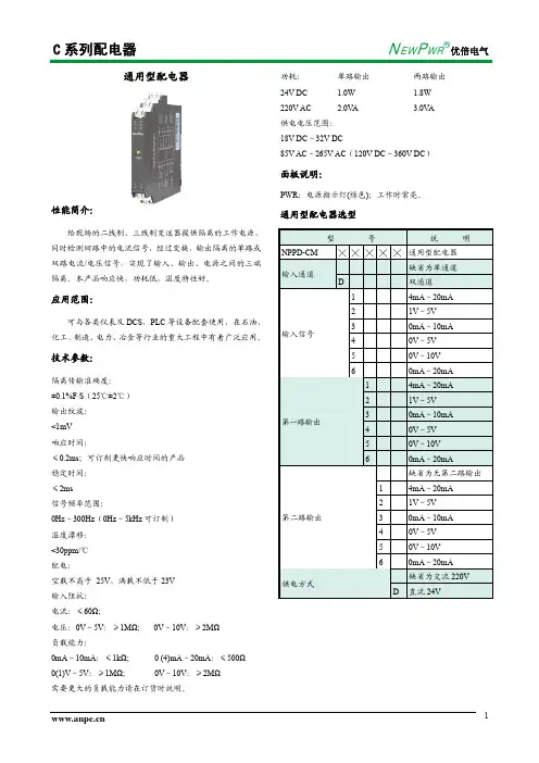
通用型配电器性能简介:给现场的二线制、三线制变送器提供隔离的工作电源,同时检测回路中的电流信号,经过变换,输出隔离的单路或双路电流/电压信号,实现了输入、输出、电源之间的三端隔离。
本产品响应快,功耗低,温度特性好。
应用范围:可与各类仪表及DCS,PLC等设备配套使用,在石油、化工、制造、电力、冶金等行业的重大工程中有着广泛应用。
技术参数:隔离传输准确度:±0.1%F·S(25℃±2℃)输出纹波:<1mV响应时间:≤0.2ms;可订制更快响应时间的产品稳定时间:≤2ms信号频率范围:0Hz~300Hz(0Hz~5kHz可订制)温度漂移:<30ppm/℃配电:空载不高于 25V,满载不低于23V输入阻抗:电流:≤60Ω;电压:0V~5V:≥1MΩ;0V~10V:≥2MΩ负载能力:0mA~10mA:≤1kΩ; 0 (4)mA~20mA:≤500Ω0(1)V~5V:≥1MΩ;0V~10V:≥2MΩ需要更大的负载能力请在订货时说明。
功耗:单路输出两路输出24VDC 1.0W1.8W 220VAC2.0V A3.0V A 供电电压范围:18V DC~32V DC85V AC~265V AC(120V DC~360V DC)面板说明:PWR:电源指示灯(绿色);工作时常亮。
通用型配电器选型型号说明NPPD-CM ╳╳╳╳╳通用型配电器缺省为单通道输入通道D双通道14mA~20mA21V~5V30mA~10mA40V~5V50V~10V输入信号60mA~20mA14mA~20mA21V~5V30mA~10mA40V~5V50V~10V第一路输出60mA~20mA缺省为无第二路输出1 4mA~20mA2 1V~5V3 0mA~10mA4 0V~5V5 0V~10V第二路输出6 0mA~20mA缺省为交流220V供电方式D 直流24V接 线 图:宽×高×深(12.8mm ×100mm ×115mm)宽×高×深(17.8mm ×100mm ×115mm) 说明:220V 供电产品的电源线接入图中电源端子L 、N 之间,L 接相线,N 接零线,PE 可靠接地。

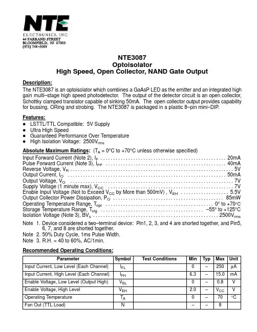
NTE3087OptoisolatorHigh Speed, Open Collector, NAND Gate Output Description:The NTE3087 is an optoisolator which combines a GaAsP LED as the emitter and an integrated high gain multi–stage high speed photodetector. The output of the detector circuit is an open collector, Schottky clamped transistor capable of sinking 50mA. The open collector output provides capability for bussing, ORing and strobing. The NTE3087 is packaged in a plastic 8–pin mini–DIP. Features:D LSTTL/TTL Compatible: 5V SupplyD Ultra High SpeedD Guaranteed Performance Over TemperatureD High Isolation Voltage: 2500V rmsAbsolute Maximum Ratings: (T A = 0°C to +70°C unless otherwise specified). . . . . . . . . . . . . . . . . . . . . . . . . . . . . . . . . . . . . . . . . . . . . . . . . .Input Forward Current (Note 2), I F20mA. . . . . . . . . . . . . . . . . . . . . . . . . . . . . . . . . . . . . . . . . . . . . . . . Pulse Forward Current (Note 3), I FP40mA . . . . . . . . . . . . . . . . . . . . . . . . . . . . . . . . . . . . . . . . . . . . . . . . . . . . . . . . . . . . . . . . . Reverse Voltage, V R5V . . . . . . . . . . . . . . . . . . . . . . . . . . . . . . . . . . . . . . . . . . . . . . . . . . . . . . . . . . . . . . . Output Current, I O50mA . . . . . . . . . . . . . . . . . . . . . . . . . . . . . . . . . . . . . . . . . . . . . . . . . . . . . . . . . . . . . . . . . Output Voltage, V O7V. . . . . . . . . . . . . . . . . . . . . . . . . . . . . . . . . . . . . . . . . . . . . . . . . . Supply Voltage (1 minute max), V CC 7V. . . . . . . . . . . . . . . . . . . Enable Input Voltage (Not to Exceed V CC by More than 500mV) , V EH 5.5V. . . . . . . . . . . . . . . . . . . . . . . . . . . . . . . . . . . . . . . . . . . . Output Collector Power Dissipation, P O85mW. . . . . . . . . . . . . . . . . . . . . . . . . . . . . . . . . . . . . . . . . . .Operating Temperature Range, T opr0° to +70°C. . . . . . . . . . . . . . . . . . . . . . . . . . . . . . . . . . . . . . . . .Storage Temperature Range, T stg –55° to +125°C. . . . . . . . . . . . . . . . . . . . . . . . . . . . . . . . . . . . . . . . . . . . . . . . . . Isolation Voltage (Note 3), BV s2500V rms Note 1.Device considered a two–terminal device: Pin1, 2, 3, and 4 are shorted together, and Pin5, 6, 7, and 8 are shorted together.Note 2.50% Duty Cycle, 1ms Pulse Width.Note 3.R.H. = 40 to 60%, AC/1min.Recommended Operating Conditions:Electrical Characteristics: (T A = 0°C to +70°C, Note 4 unless otherwise specified)Note 4.All typical values at V CC = 5V, T A = +25°C.Switching Characteristics: (T A = +25°C, V CC = 5V unless otherwise specified)Truth Table: (0.1µF bypass capacitor must be connected between Pin8 and Pin5)。
Si86xx 1 Mbps Data Sheet 1 Mbps, 2.5 kV RMS Digital IsolatorsSkyworks' family of ultra-low-power digital isolators are CMOS devices offering substan-tial data rate, propagation delay, power, size, reliability, and external BOM advantages over legacy isolation technologies. The operating parameters of these products remain stable across wide temperature ranges and throughout device service life for ease of design and highly uniform performance. All device versions have Schmitt trigger inputs for high noise immunity and only require VDD bypass capacitors.All products support Data rates up to 1 Mbps and Enable inputs which provide a single point control for enabling and disabling output drive. All products are safety certified by UL, CSA, VDE, and CQC and support withstand ratings up to 2.5 kV RMS.Automotive Grade is available for certain part numbers. These products are built using automotive-specific flows at all steps in the manufacturing process to ensure the robust-ness and low defectivity required for automotive applications.KEY FEATURES•High-speed operation•DC to 1 Mbps•No start-up initialization required•Wide Operating Supply Voltage•2.5 to 5.5 V•Up to 2500 V RMS isolation•60-year life at rated working voltage •High electromagnetic immunity•Ultra low power (typical)•5 V Operation: 1.6 mA per channel at 1Mbps•2.5 V Operation: 1.5 mA per channel at1 Mbps•Tri-state outputs with ENABLE •Schmitt trigger inputs•Transient Immunity 50 kV/µs•AEC-Q100 qualification•Wide temperature range•–40 to 125 °C•RoHS-compliant packages•SOIC-16 wide body•SOIC-16 narrow body•SOIC-8 narrow body•Automotive-grade OPNs available•AIAG compliant PPAP documentationsupport•IMDS and CAMDS listing supportIndustrial Applications•Industrial automation systems •Medical electronics•Isolated switch mode supplies •Isolated ADC, DAC•Motor control•Power inverters •Communication systemsSafety Regulatory Approvals•UL 1577 recognized•Up to 5000 V RMS for 1 minute •CSA component notice 5A approval •IEC 60950-1, 61010-1•VDE certification conformity•IEC 60747-5-2 (VDE0884 Part 2)•CQC certification approval•GB4943.1Automotive Applications•On-board chargers •Battery management systems •Charging stations •Traction inverters•Hybrid Electric Vehicles •Battery Electric Vehicles1. Ordering GuideIndustrial and Automotive Grade OPNsIndustrial-grade devices (part numbers having an “-I” in their suffix) are built using well-controlled, high-quality manufacturing flows to ensure robustness and reliability. Qualifications are compliant with JEDEC, and defect reduction methodologies are used throughout definition, design, evaluation, qualification, and mass production steps.Automotive-grade devices (part numbers having an “-A” in their suffix) are built using automotive-specific flows at all steps in the manufacturing process to ensure robustness and low defectivity. These devices are supported with AIAG-compliant Production Part Approval Process (PPAP) documentation, and feature International Material Data System (IMDS) and China Automotive Material Data System (CAMDS) listing. Qualifications are compliant with AEC-Q100, and a zero-defect methodology is maintained throughout definition, design, evaluation, qualification, and mass production steps.Table 1.1. Ordering Guide for Valid OPNs1, 2, 4Table of Contents1. Ordering Guide (2)2. Functional Description (5)2.1 Theory of Operation (5)3. Device Operation (6)3.1 Device Startup (8)3.2 Undervoltage Lockout (8)3.3 Layout Recommendations (8)3.3.1 Supply Bypass (8)3.3.2 Output Pin Termination (8)4. Electrical Specifications (9)5. Pin Descriptions (30)5.1 Pin Descriptions (Si861x/2x Narrow Body SOIC-8) (30)5.2 Pin Descriptions (Si863x) (31)5.3 Pin Descriptions (Si864x) (32)5.4 Pin Descriptions (Si8650/51/52) (33)5.5 Pin Descriptions (Si866x) (34)6. Package Outlines (35)6.1 Package Outline (16-Pin Wide Body SOIC) (35)6.2 Package Outline (16-Pin Narrow Body SOIC) (37)6.3 Package Outline (8-Pin Narrow Body SOIC) (39)7. Land Patterns (40)7.1 Land Pattern (16-Pin Wide-Body SOIC) (40)7.2 Land Pattern (16-Pin Narrow Body SOIC) (41)7.3 Land Pattern (8-Pin Narrow Body SOIC) (42)8. Top Markings (43)8.1 Top Marking (16-Pin Wide Body SOIC) (43)8.2 Top Marking (16-Pin Narrow Body SOIC) (44)8.3 Top Marking (8-Pin Narrow Body SOIC) (45)9. Revision History (46)Si86xx 1 Mbps Data Sheet • Functional Description2. Functional Description2.1 Theory of OperationThe operation of an Si86xx channel is analogous to that of an opto coupler, except an RF carrier is modulated instead of light. This simple architecture provides a robust isolated data path and requires no special considerations or initialization at start-up. A simplified block diagram for a single Si86xx channel is shown in the figure below.A BFigure 2.1. Simplified Channel DiagramA channel consists of an RF Transmitter and RF Receiver separated by a semiconductor-based isolation barrier. Referring to the Transmitter, input A modulates the carrier provided by an RF oscillator using on/off keying. The Receiver contains a demodulator that decodes the input state according to its RF energy content and applies the result to outputB via the output driver. This RF on/off keying scheme is superior to pulse code schemes as it provides best-in-class noise immunity, low power consumption, and better immunity to magnetic fields. See the figure below for more details.Input SignalModulation SignalOutput SignalFigure 2.2. Modulation Scheme3. Device OperationDevice behavior during start-up, normal operation, and shutdown is shown in Figure 3.1 Device Behavior during Normal Operation on page 8, where UVLO+ and UVLO- are the positive-going and negative-going thresholds respectively. Refer to the table below to determine outputs when power supply (VDD) is not present. Additionally, refer to Table 3.2 Enable Input Truth1on page 7for logic conditions when enable pins are used.Table 3.1. Si86xx Logic OperationTable 3.2. Enable Input Truth13.1 Device StartupOutputs are held low during powerup until VDD is above the UVLO threshold for time period tSTART. Following this, the outputs follow the states of inputs.3.2 Undervoltage LockoutUndervoltage Lockout (UVLO) is provided to prevent erroneous operation during device startup and shutdown or when VDD is below its specified operating circuits range. Both Side A and Side B each have their own undervoltage lockout monitors. Each side can enter or exit UVLO independently. For example, Side A unconditionally enters UVLO when V DD1 falls below V DD1(UVLO–) and exits UVLO when V DD1 rises above V DD1(UVLO+). Side B operates the same as Side A with respect to its V DD2 supply.VVFigure 3.1. Device Behavior during Normal Operation3.3 Layout RecommendationsTo ensure safety in the end user application, high voltage circuits (i.e., circuits with >30 V AC) must be physically separated from the safety extra-low voltage circuits (SELV is a circuit with <30 V AC) by a certain distance (creepage/clearance). If a component, such as a digital isolator, straddles this isolation barrier, it must meet those creepage/clearance requirements and also provide a sufficiently large high-voltage breakdown protection rating (commonly referred to as working voltage protection). Table 4.5 Regulatory Information1 on page 25and Table 4.6 Insulation and Safety-Related Specifications on page 25detail the working voltage and creepage/clearance capabilities of the Si86xx. These tables also detail the component standards (UL1577, IEC60747, CSA 5A), which are readily accepted by certification bodies to provide proof for end-system specifications requirements. Refer to the end-system specification (61010-1, 60950-1, 60601-1, etc.) requirements before starting any design that uses a digital isolator.3.3.1 Supply BypassThe Si86xx family requires a 0.1 µF bypass capacitor between V DD1 and GND1 and V DD2 and GND2. The capacitor should be placed as close as possible to the package. To enhance the robustness of a design, the user may also include resistors (50–300 Ω ) in series with the inputs and outputs if the system is excessively noisy.3.3.2 Output Pin TerminationThe nominal output impedance of an isolator driver channel is approximately 50 Ω, ±40%, which is a combination of the value of the on-chip series termination resistor and channel resistance of the output driver FET. When driving loads where transmission line effects will be a factor, output pins should be appropriately terminated with controlled impedance PCB traces.4. Electrical SpecificationsTable 4.1. Recommended Operating ConditionsTable 4.2. Electrical Characteristics(V DD1 = 5 V±10%, V DD2 = 5 V±10%, T A = –40 to 125 °C)ENABLEOUTPUTSen1t en2Figure 4.1. ENABLE Timing DiagramInputOutputFigure 4.2. Propagation Delay TimingFigure 4.3. Common-Mode Transient Immunity Test CircuitTable 4.3. Electrical Characteristics(V DD1 = 3.3 V±10%, V DD2 = 3.3 V±10%, T A = –40 to 125 °C)Table 4.4. Electrical Characteristics (V DD1 = 2.5 V ±5%, V DD2 = 2.5 V ±5%, T A = –40 to 125 °C)Table 4.5. Regulatory Information1CSAThe Si86xx is certified under CSA Component Acceptance Notice 5A, IEC61010-1 and IEC60950-1. For more details, see File 232873.VDEThe Si86xx is certified according to IEC 60747-5-2. For more details, see File 5006301-4880-0001.ULThe Si86xx is certified under UL1577 component recognition program. For more details, see File E257455.CQCThe Si86xx is certified under GB4943.1-2011. For more details, see certificates CQC130******** and CQC130********.Note:1.Regulatory Certifications apply to2.5 kV RMS rated devices which are production tested to3.0 kV RMS for 1 sec.For more information, see 5.5 Pin Descriptions (Si866x).Table 4.6. Insulation and Safety-Related SpecificationsTable 4.7. IEC 60664-1 (VDE 0844 Part 2) RatingsTable 4.8. IEC 60747-5-2 Insulation Characteristics for Si86xxxx*Table 4.9. IEC Safety Limiting Values1Table 4.10. Thermal Characteristics200150100505004002001000Temperature (ºC)S a f e t y -L i m i t i n g C u r r e n t (m A )300Figure 4.4. (WB SOIC-16) Thermal Derating Curve, Dependence of Safety Limiting Valueswith Case Temperature per DIN EN 60747-5-2200150100505004002001000Temperature (ºC)S a f e t y -L i m i t i n g C u r r e n t (m A )300Figure 4.5. (NB SOIC-16) Thermal Derating Curve, Dependence of Safety Limiting Valueswith Case Temperature per DIN EN 60747-5-2200150********2001000Case Temperature (ºC)S a f e t y -L i m i t i n g V a l u e s (m A )300Figure 4.6. (NB SOIC-8) Thermal Derating Curve, Dependence of Safety Limiting Valueswith Case Temperature per DIN EN 60747-5-2Table 4.11. Absolute Maximum Ratings 15. Pin Descriptions5.1 Pin Descriptions (Si861x/2x Narrow Body SOIC-8)V DD2 V DD1V DD2V DD2Figure 5.1. Si861x/2x Narrow Body SOIC-8 Pin DescriptionsTable 5.1. Si861x/2x Narrow Body SOIC-8 Pin DescriptionsSi86xx 1 Mbps Data Sheet • Pin DescriptionsVDD2VDD2Figure 5.2. Si863x Pin DescriptionsTable 5.2. Si863x Pin DescriptionsVDD2VDD2V DD2Figure 5.3. Si864x Pin DescriptionsTable 5.3. Si864x Pin Descriptions5.4 Pin Descriptions (Si8650/51/52)VDD2VDD2V DD2Figure 5.4. Si865x Pin DescriptionsTable 5.4. Si865x Pin Descriptions5.5 Pin Descriptions (Si866x)VVVVFigure 5.5. Si866x Pin DescriptionsTable 5.5. Si866x Pin Descriptions6. Package Outlines6.1 Package Outline (16-Pin Wide Body SOIC)The figure below illustrates the package details for the Si86xx Digital Isolator. The table below lists the values for the dimensions shown in the illustration.Figure 6.1. 16-Pin Wide Body SOICTable 6.1. Package Diagram Dimensions6.2 Package Outline (16-Pin Narrow Body SOIC)The figure below illustrates the package details for the Si86xx in a 16-pin narrow-body SOIC (SO-16). The table below lists the values for the dimensions shown in the illustration.Figure 6.2. 16-pin Small Outline Integrated Circuit (SOIC) PackageTable 6.2. Package Diagram Dimensions6.3 Package Outline (8-Pin Narrow Body SOIC)The figure below illustrates the package details for the Si86xx. The table below lists the values for the dimensions shown in the illustration.Figure 6.3. 8-pin Small Outline Integrated Circuit (SOIC) PackageTable 6.3. Package Diagram Dimensions7. Land Patterns7.1 Land Pattern (16-Pin Wide-Body SOIC)The figure below illustrates the recommended land pattern details for the Si86xx in a 16-pin wide-body SOIC. The table below lists the values for the dimensions shown in the illustration.Figure 7.1. 16-Pin SOIC Land PatternTable 7.1. 16-Pin Wide Body SOIC Land Pattern DimensionsTable 7.2. 16-Pin Narrow Body SOIC Land Pattern DimensionsTable 7.3. PCM Land Pattern Dimensions (8-Pin Narrow Body SOIC)8. Top Markings8.1 Top Marking (16-Pin Wide Body SOIC)Figure 8.1. 16-Pin Wide Body SOICTable 8.1. Top Marking Explanation (16-Pin Wide Body SOIC)Line 1 Marking:Base Part NumberOrdering Options(See 1. Ordering Guide for more information).Si86 = Isolator product seriesXY = Channel ConfigurationX = # of data channels (5, 4, 3, 2, 1)Y = # of reverse channels (2, 1, 0)S = Speed Grade (max data rate) and operating mode:A = 1 Mbps (default output = low)B = 150 Mbps (default output = low)D = 1 Mbps (default output = high)E = 150 Mbps (default output = high)V = Insulation ratingA = 1 kV;B = 2.5 kV;C = 3.75 kV;D = 5.0 kVLine 2 Marking:YY = YearWW = Workweek Assigned by assembly subcontractor. Corresponds to the year and work week of the mold date.RTTTTT = Mfg Code Manufacturing code from assembly house“R” indicates revisionLine 3 Marking:Circle = 1.7 mm Diameter(Center-Justified)“e4” Pb-free symbolCountry of Origin ISO Code Abbreviation CC = Country of Origin ISO Code Abbreviation•TW = Taiwan•TH = ThailandFigure 8.2. 16-Pin Narrow Body SOICTable 8.2. Top Marking Explanation (16-Pin Narrow Body SOIC)Line 1 Marking:Base Part NumberOrdering Options(See 1. Ordering Guide for more information.)Si86 = Isolator product seriesXY = Channel ConfigurationX = # of data channels (5, 4, 3, 2, 1)Y = # of reverse channels (2, 1, 0)S = Speed Grade (max data rate) and operating mode:A = 1 Mbps (default output = low)B = 150 Mbps (default output = low)D = 1 Mbps (default output = high)E = 150 Mbps (default output = high)V = Insulation ratingA = 1 kV;B = 2.5 kV;C = 3.75 kVLine 2 Marking:Circle = 1.2 mm Diameter“e3” Pb-Free SymbolYY = YearWW = Work Week Assigned by the assembly subcontractor. Corresponds to the year and work week of the mold date.RTTTTT = Mfg Code Manufacturing code from assembly house“R” indicates revisionFigure 8.3. 8-Pin Narrow Body SOICTable 8.3. Top Marking Explanation (8-Pin Narrow Body SOIC)Line 1 Marking:Base Part NumberOrdering Options(See 1. Ordering Guide for more information).Si86 = Isolator Product Series XY = Channel ConfigurationS = Speed Grade (max data rate) V = Insulation ratingLine 2 Marking:YY = YearWW = Workweek Assigned by assembly subcontractor. Corresponds to the year and workweek of the mold date.R = Product RevisionT = First character of the manufacturing codeLine 3 Marking:Circle = 1.1 mm Diameter“e3” Pb-Free Symbol.TTTT = Last four characters of the manufactur-ing codeLast four characters of the manufacturing code.9. Revision HistoryRevision 1.03September 2019•Updated Ordering Guide.Revision 1.02February 2018•Added SI8641AB-AS1 and SI8642AB-AS1 to Ordering Guide for Automotive-Grade OPN options Revision 1.01January 2018•Updated data sheet format.•Added new table to Ordering Guide for Automotive-Grade OPN options•Updated Table 4.5 Regulatory Information1 on page 25.•Added CQC certificate numbers.•Updated 1. Ordering Guide.•Removed references to moisture sensitivity levels.•Removed note 2.Copyright © 2021 Skyworks Solutions, Inc. All Rights Reserved.Information in this document is provided in connection with Skyworks Solutions, Inc. (“Skyworks”) products or services. These materials, including the information contained herein, are provided by Skyworks as a service to its customers and may be used for informational purposes only by the customer. Skyworks assumes no responsibility for errors or omissions in these materials or the information contained herein. Skyworks may change its documentation, products, services, specifications or product descriptions at any time, without notice. Skyworks makes no commitment to update the materials or information and shall have no responsibility whatsoever for conflicts, incompatibilities, or other difficulties arising from any future changes.No license, whether express, implied, by estoppel or otherwise, is granted to any intellectual property rights by this document. Skyworks assumes no liability for any materials, products or information provided hereunder, including the sale, distribution, reproduction or use of Skyworks products, information or materials, except as may be provided in Skyworks’ Terms and Conditions of Sale.THE MATERIALS, PRODUCTS AND INFORMATION ARE PROVIDED “AS IS” WITHOUT WARRANTY OF ANY KIND, WHETHER EXPRESS, IMPLIED, STATUTORY, OR OTHERWISE, INCLUDING FITNESS FOR A PARTICULAR PURPOSE OR USE, MERCHANTABILITY, PERFORMANCE, QUALITY OR NON-INFRINGEMENT OF ANY INTELLECTUAL PROPERTY RIGHT; ALL SUCH WARRANTIES ARE HEREBY EXPRESSLY DISCLAIMED. SKYWORKS DOES NOT WARRANT THE ACCURACY OR COMPLETENESS OF THE INFORMATION, TEXT, GRAPHICS OR OTHER ITEMS CONTAINED WITHIN THESE MATERIALS. SKYWORKS SHALL NOT BE LIABLE FOR ANY DAMAGES, INCLUDING BUT NOT LIMITED TO ANY SPECIAL, INDIRECT, INCIDENTAL, STATUTORY, OR CONSEQUENTIAL DAMAGES, INCLUDING WITHOUT LIMITATION, LOST REVENUES OR LOST PROFITS THAT MAY RESULT FROM THE USE OF THE MATERIALS OR INFORMATION, WHETHER OR NOT THE RECIPIENT OF MATERIALS HAS BEEN ADVISED OF THE POSSIBILITY OF SUCH DAMAGE.Skyworks products are not intended for use in medical, lifesaving or life-sustaining applications, or other equipment in which the failure of the Skyworks products could lead to personal injury, death, physical or environmental damage. Skyworks customers using or selling Skyworks products for use in such applications do so at their own risk and agree to fully indemnify Skyworks for any damages resulting from such improper use or sale.Customers are responsible for their products and applications using Skyworks products, which may deviate from published specifications as a result of design defects, errors, or operation of products outside of published parameters or design specifications. Customers should include design and operating safeguards to minimize these and other risks. Skyworks assumes no liability for applications assistance, customer product design, or damage to any equipment resulting from the use of Skyworks products outside of Skyworks’ published specifications or parameters.Skyworks, the Skyworks symbol, Sky5®, SkyOne ®, SkyBlue™, Skyworks Green™, Clockbuilder ®, DSPLL ®, ISOmodem ®, ProSLIC ®, and SiPHY ® are trademarks or registered trademarks of Skyworks Solutions, Inc. or its subsidiaries in the United States and other countries. Third-party brands and names are for identification purposes only and are the property of their respective owners. Additional information, including relevant terms and conditions, posted at , are incorporated by reference.PortfolioQuality/qualitySupport & Resources/support。
通用型隔离器性能简介:输入电流/电压信号,变送输出隔离的电流/电压信号,实现了输入、输出与电源之间的三端隔离;本产品响应快,功耗低,温度特性好。
应用范围:可与各类仪表及DCS,PLC等设备配套使用,在石油、化工、制造、电力、冶金等行业的重大工程中有着广泛应用。
技术参数:隔离传输准确度:±0.1%F·S(25℃±2℃)输出纹波:<1mV响应时间:≤0.2ms;可订制更快响应时间的产品稳定时间:≤2ms信号频率范围:0Hz~300Hz(0Hz~5kHz可订制)温度漂移:<30ppm/℃输入阻抗:电流:≤60Ω;电压:0V~5V:≥1MΩ;0V~10V:≥2MΩ负载能力:0mA~10mA:≤600Ω;; 0(4)mA~20mA:≤300Ω-10mA~+10mA:≤1kΩ; -20mA~+20mA:≤500Ω0(1)V~5V:≥1MΩ;0V~10V:≥2MΩ-5V~+5V:≥1MΩ; -10V~+10V:≥2MΩ需要更大的负载能力请在订货时说明。
功耗:单路输出两路输出24VDC 0.4W0.6W220VAC1.0V A 1.2V A供电电压范围:18V DC~32V DC85V AC~265V AC(120V DC~360V DC)面板说明:PWR:电源指示灯(绿色);工作时常亮。
通用型隔离器选型型号说明NPGL-CM ╳╳╳╳╳通用型隔离器缺省为单通道输入通道D双通道1 4mA~20mA2 1V~5V3 0mA~10mA3E -10mA~10mA4 0V~5V4E -5V~5V5 0V~10V5E -10V~10V6 0mA~20mA输入信号6E -20mA~20mA14mA~20mA21V~5V30mA~10mA3E-10mA~10mA40V~5V4E-5V~5V50V~10V5E-10V~10V60mA~20mA第一路输出6E-20mA~20mA缺省为无第二路输出1 4mA~20mA21V~5V3 0mA~10mA3E -10mA~10mA40V~5V4E -5V~5V50V~10V5E -10V~10V6 0mA~20mA第二路输出6E -20mA~20mA缺省为交流220V供电方式D 直流24V选型说明:正负信号输出的产品仅支持一入一出。
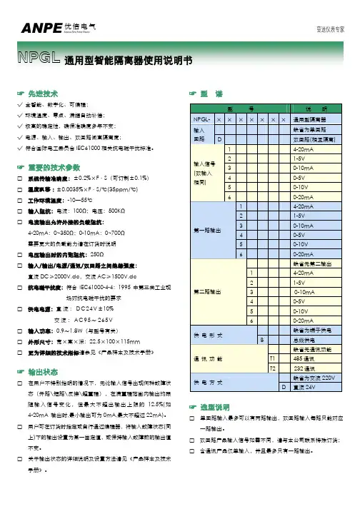
智能型隔离器时间:2010-4-20 14:25:01 作者:本站编辑:admins 访问次数:9781【关闭】智能隔离器:输入单通道或双通道电流或电压信号,变送输出隔离的单路或双路电流或电压信号,并提高输入、输出、电源之间的电气隔离性能。
隔离器技术特点:本产品采用了先进的数字技术,具备了传统模拟隔离器所不具备的多项先进性能,在对高、低频干扰信号的抑制方面均有着优异表现,即使在大功率控制系统中依然能够可靠应用,内部采用数字化调校、无零点及满度电位器、自动动态校准零点、温度漂移自动补偿等诸多先进技术,并符合IEC61000-4-4:1995中所规定的第四类(恶劣工业现场)环境对产品的抗电磁干扰要求,这一系列技术的应用使产品的稳定性及可靠性得到科学的保证。
隔离器适用性:可与单元组合仪表及DCS,PLC等系统配套使用,在油田、石化、制造、电力、冶金等行业的重大工程中有着广泛应用。
隔离器技术参数:隔离器系统传输准确度:±0.1%×F•S隔离器温度飘移:±0.0035%×F•S/℃(35ppm/℃)输入阻抗:电流:≤60Ω;电压:≥500KΩ电流输出允许外接的负载阻抗:4-20mA输出时0~300Ω;0-10mA输出时0~600Ω,0(1)-5V:≥500KΩ; 0-10V:≥1MΩ需要更大的负载能力请在订货时说明。
隔离器供电电源:AC 95~265VDC 20~32V输入功率:0.9~1.8W(与型号有关,详见产品手册附录中关于输入功率的计算方法)隔离器输入信号断线时的输出状态:隔离器输出状态有跟随方式、报警方式两种状态可设置隔离器选型:通用型智能隔离器选型说明:1.单通道产品最多可以有两路输出;双通道产品每路只能对应一路输出。
2.双通道产品输入信号如需不同,请与本公司联系订货.3.含通讯产品仅单输入通道产品,并且最多只有一路模拟信号输出。
隔离器面板指示:PWR:电源指示灯(绿色);ALM:输入信号报警指示灯(红色);隔离器正常工作状态时该指示灯不亮;隔离器输入信号故障时闪烁;输入信号超量程时长亮。
通用型隔离器
性能简介:
输入电流/电压信号,变送输出隔离的电流/电压信号,实现了输入、输出与电源之间的三端隔离;本产品响应快,功耗低,温度特性好。
应用范围:
可与各类仪表及DCS,PLC等设备配套使用,在石油、化工、制造、电力、冶金等行业的重大工程中有着广泛应用。
技术参数:
隔离传输准确度:
±0.1%F·S(25℃±2℃)
输出纹波:
<1mV
响应时间:
≤0.2ms;可订制更快响应时间的产品
稳定时间:
≤2ms
信号频率范围:
0Hz~300Hz(0Hz~5kHz可订制)
温度漂移:
<30ppm/℃
输入阻抗:
电流:≤60Ω;
电压:0V~5V:≥1MΩ;0V~10V:≥2MΩ
负载能力:
0mA~10mA:≤600Ω;; 0(4)mA~20mA:≤300Ω
-10mA~+10mA:≤1kΩ; -20mA~+20mA:≤500Ω
0(1)V~5V:≥1MΩ;0V~10V:≥2MΩ
-5V~+5V:≥1MΩ; -10V~+10V:≥2MΩ
需要更大的负载能力请在订货时说明。
功耗:单路输出两路输出
24V
DC 0.4W
0.6W
220V
AC
1.0V A 1.2V A
供电电压范围:
18V DC~32V DC
85V AC~265V AC(120V DC~360V DC)面板说明:
PWR:电源指示灯(绿色);工作时常亮。
通用型隔离器选型
型
号说明NPGL-CM ╳╳╳╳╳通用型隔离器
缺省为单通道
输入通道
D双通道
1 4mA~20mA
2 1V~5V
3 0mA~10mA
3E -10mA~10mA
4 0V~5V
4E -5V~5V
5 0V~10V
5E -10V~10V
6 0mA~20mA
输入信号
6E -20mA~20mA
14mA~20mA
21V~5V
30mA~10mA
3E-10mA~10mA
40V~5V
4E-5V~5V
50V~10V
5E-10V~10V
60mA~20mA
第一路输出
6E-20mA~20mA
缺省为无第二路输出
1 4mA~20mA
21V~5V
3 0mA~10mA
3E -10mA~10mA
40V~5V
4E -5V~5V
50V~10V
5E -10V~10V
6 0mA~20mA
第二路输出
6E -20mA~20mA
缺省为交流220V
供电方式
D 直流24V
选型说明:正负信号输出的产品仅支持一入一出。
接 线 图:
宽×高×深(12.8mm ×100mm ×115mm)
宽×高×深(17.8mm ×100mm ×115mm)
说 明:
1、 220V 供电产品的电源线接入图中电源端子L 、N 之间,
L 接相线,N 接零线,PE 可靠接地。
2、 正负信号输入输出产品的接线图直接参考产品说明书。
输入
24V 供电,双路输入,两路电流/电压输出
输入输入输出 1输出 2220V 供电,双路输入,两路电流/电压输出。