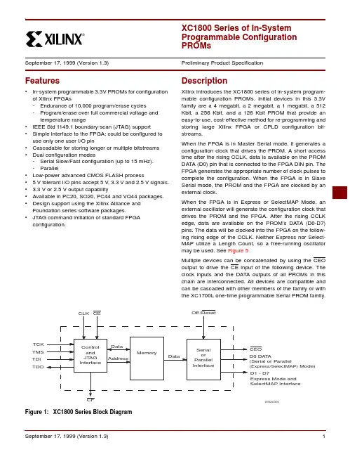
Features•In-system programmable 3.3V PROMs for configuration of Xilinx FPGAs-Endurance of 10,000 program/erase cycles-Program/erase over full commercial voltage and temperature range•IEEE Std 1149.1 boundary-scan (JTAG) support •Simple interface to the FPGA; could be configured to use only one user I/O pin•Cascadable for storing longer or multiple bitstreams •Dual configuration modes-Serial Slow/Fast configuration (up to 15 mHz).-Parallel•Low-power advanced CMOS FLASH process• 5 V tolerant I/O pins accept 5 V, 3.3 V and 2.5 V signals.• 3.3 V or 2.5 V output capability•Available in PC20, SO20, PC44 and VQ44 packages.•Design support using the Xilinx Alliance and Foundation series software packages.•JTAG command initiation of standard FPGA configuration.DescriptionXilinx introduces the XC1800 series of in-system program-mable configuration PROMs. Initial devices in this 3.3V family are a 4 megabit, a 2 megabit, a 1 megabit, a 512 Kbit, a 256 Kbit, and a 128 Kbit PROM that provide an easy-to-use, cost-effective method for re-programming and storing large Xilinx FPGA or CPLD configuration bit-streams.When the FPGA is in Master Serial mode, it generates a configuration clock that drives the PROM. A short access time after the rising CCLK, data is available on the PROM DATA (D0) pin that is connected to the FPGA DIN pin. The FPGA generates the appropriate number of clock pulses to complete the configuration. When the FPGA is in Slave Serial mode, the PROM and the FPGA are clocked by an external clock.When the FPGA is in Express or SelectMAP Mode, an external oscillator will generate the configuration clock that drives the PROM and the FPGA. After the rising CCLK edge, data are available on the PROM’s DATA (D0-D7) pins. The data will be clocked into the FPGA on the follow-ing rising edge of the CCLK. Neither Express nor Select-MAP utilize a Length Count, so a free-running oscillator may be used. See Figure5Multiple devices can be concatenated by using the CEO output to drive the CE input of the following device. The clock inputs and the DATA outputs of all PROMs in this chain are interconnected. All devices are compatible and can be cascaded with other members of the family or with the XC1700L one-time programmable Serial PROM family.September 17, 1999 (Version 1.3)Preliminary Product Specification Figure 1: XC1800 Series Block DiagramPinout and Pin Description Table 1: Pin Names and DescriptionsPin Name BoundaryScanOrderFunction Pin Description44-pinVQFP44-pinPLCC20-pinSOIC & PLCCD04DATA OUT D0 is the DATA output pin to provide datafor configuring an FPGA in serial mode.40213OUTPUTENABLED16DATA OUT D0- D7 are the output pins to provide par-allel data for configuring a Xilinx FPGA inexpress mode.2935165OUTPUTENABLED22DATA OUT4242 1OUTPUTENABLED38DATA OUT273315 7OUTPUTENABLED424DATA OUT9157* 23OUTPUTENABLED510DATA OUT253114 9OUTPUTENABLED617DATA OUT14209 16OUTPUTENABLED714DATA OUT192512 13OUTPUTENABLECLK0DATA IN Each rising edge on the CLK input incre-ments the internal address counter if bothCE is low and OE/RESET is high.4353OE/ RESET 20DATA IN When Low, this input holds the addresscounter reset and the DATA output athigh impedance. 13198 19DATA OUT18OUTPUTENABLECE15DATA IN When CE is High, this pin puts the deviceinto standby mode. The DATA output pinis at High impedance, and the device is inlow power standby mode.152110CF22DATA OUT Allows JTAG CONFIG instruction to ini-tiate FPGA configuration without power-ing down FPGA.10167*21DATA IN*Programmable for Serial Mode only on 18512 and 1801.CEO13DATA OUT Chip Enable (CEO) output is connectedto the CE input of the next PROM in thechain. This output is Low when the CEand OE/RESET inputs are active AND the internal address counter has been in-cremented beyond its Terminal Count (TC) value. When the PROM has been read, CEO will follow CE as long as OE/RESET is High. When OE/RESET goes Low, CEO stays High until the PROM is brought out of reset by bringing OE/RE-SET High. CEO can be programmed to be either active High or active Low.21271314OUTPUTENABLEGND GND is the ground connection.6, 18, 28 & 413, 12, 24 &3411TMSMODE SELECTThe state of TMS on the rising edge of TCK determines the state transitions at the Test Access Port (TAP) controller. TMS has an internal 50K ohm resistive pull-up on it to provide a logic 1 to the de-vice if the pin is not driven.5115TCK CLOCK This pin is the JTAG test clock. It se-quences the TAP controller and all the JTAG test and programming electronics.7136TDI DATA IN This pin is the serial input to all JTAG in-struction and data registers. TDI has an internal 50K ohm resistive pull-up on it to provide a logic 1 to the system if the pin is not driven.394TDODATA OUT This pin is the serial output for all JTAGinstruction and data registers. TDO has an internal 50k ohm resistive pull-up on it to provide a logic 1 to the system if the pin is not driven.313717V CC Positive voltage supply of 3.3V for inter-nal logic and input buffers.17, 35 & 3823, 41 & 4418 & 20V CCOPositive voltage supply connected to the output voltage drivers.8, 16, 26 & 3614, 22, 32 & 4219Pin Name Boundary Scan OrderFunctionPin Description44-pin VQFP 44-pin PLCC 20-pin SOIC & PLCCXilinx FPGAs and CompatiblePROMsCapacityDevice Configuration Bits PROM XC4003E53,984XC18128 XC4005E95,008XC18128 XC4006E119,840XC18128 XC4008E147,552XC18256 XC4010E178,144XC18256 XC4013E247,968XC18256 XC4020E329,312XC18512 XC4025E422,176XC18512 XC4002XL61,100XC18128 XC4005XL151,960XC18256 XC4010XL283,424XC18512 XC4013XL/XLA393,632XC18512 XC4020XL/XLA521,880XC18512 XC4028XL/XLA668,184XC1801 XC4036XL/XLA832,528XC1801 XC4044XL/XLA1,014,928XC1801 XC4052XL/XLA1,215,368XC1802 XC4062XL/XLA1,433,864XC1802 XC4085XL/XLA1,924,992XC1802 XC40110XV2,686,136XC1804 XC40150XV3,373,448XC1804 XC40200XV4,551,056XC1804 +XC18512 XC40250XV5,433,888XC1804 +XC1802 XCV50559,232XC1801 XCV100781,248XC1801 XCV1501,041,128XC1801 XCV2001,335,872XC1802 XCV3001,751,840XC1802 XCV4002,546,080XC1804 XCV6003,608,000XC1804 XCV8004,715,648XC1804 +XC18512 XCV10006,127,776XC1804 +XC1802Devices Configuration Bits 18044,194,304 18022,097,152 18011,048,576 18512524,288 18256262,144 18128131,072In-System ProgrammingOne or more in-system programmable PROMs can be daisy chained together and programmed in-system via the standard 4-pin JTAG protocol as shown in Figure2. In-sys-tem programming offers quick and efficient design itera-tions and eliminates unnecessary package handling or socketing of devices. The Xilinx development system pro-vides the programming data sequence using Xilinx JTAG Programmer software and a download cable, a third-party JTAG development system, a JTAG-compatible board tester, or a simple microprocessor interface that emulates the JTAG instruction sequence.All outputs are 3-stated or held at clamp levels during in-system programming.External ProgrammingXilinx reprogrammable PROMs can also be programmed by the Xilinx HW-130 device programmer. This provides the added flexibility of using pre-programmed devices in design, boundary-scan manufacturing tools, with an in-sys-tem programmable option for future enhancements and design changes.Reliability and EnduranceXilinx in-system programmable products provide a mini-mum endurance level of 10,000 in-system program/erase cycles and a minimum data retention of 10 years. Each device meets all functional, performance, and data reten-tion specifications within this endurance limit.Design SecurityThe Xilinx in-system programmable PROM devices incor-porate advanced data security features to fully protect the programming data against unauthorized reading. Table2 shows the security setting available.The read security bit can be set by the user to prevent the internal programming pattern from being read or copied via JTAG. When set it allows device erase. Erasing the entire device is the only way to reset the read security bit.Table 2: Data Security OptionsDefault SetRead AllowedProgram/Erase AllowedRead Inhibited via JTAGErase AllowedX5902(a)(b)Figure 2: In-System Programming Operation (a) solder device to PCB and (b) Program using Download CableIEEE 1149.1 Boundary-Scan (JTAG) The XC1800 family is fully compliant with the IEEE Std. 1149.1 Boundary-Scan, also known as JTAG. A Test Access Port (TAP) and registers are provided to support all required boundary scan instructions, as well as many of the optional instructions specified by IEEE Std. 1149.1. In addi-tion, the JTAG interface is used to implement in-system programming (ISP) to facilitate configuration, erasure, and verification operations on the XC1800 device.Table3 lists the required and optional boundary-scan instructions supported in the XC1800. Refer to the IEEE Std. 1149.1 specification for a complete description of boundary-scan architecture and the required and optional instructions.Table 3: Boundary Scan InstructionsInstruction RegisterThe Instruction Register (IR) for the XC1800 is 8-bits wide and is connected between TDI and TDO during an instruc-tion scan sequence. In preparation for an instruction scan sequence, the instruction register is parallel loaded with a fixed instruction capture pattern. This pattern is shifted out onto TDO (LSB first), while an instruction is shifted into the instruction register from TDI. The detailed composition of the instruction capture pattern is illustrated in Figure 3. The ISP Status field, IR(4), contains logic 1 if the device is currently in ISP mode; otherwise, it will contain 0. The Security field, IR(3), will contain logic 1 if the device has been programmed with the security option turned on; other-wise, it will contain 0.Figure 3: Instruction Register values loaded into IR as part of an instruction scan sequenceBoundary Scan RegisterThe boundary-scan register is used to control and observe the state of the device pins during the EXTEST, SAMPLE/ PRELOAD, and CLAMP instructions. Each output pin on the XC1800 has two register stages that contribute to the boundary-scan register, while each input pin only has one register stage.For each output pin, the register stage nearest to TDI con-trols and observes the output state, and the second stage closest to TDO controls and observes the 3-state enable state of the pin.For each input pin, the register stage controls and observes the input state of the pin.Identification RegistersThe IDCODE is a fixed, vendor-assigned value that is used to electrically identify the manufacturer and type of the device being addressed. The IDCODE register is 32-bits wide. The IDCODE register can be shifted out for examina-tion by using the IDCODE instruction.The IDCODE register has the following binary format: vvvv:ffff:ffff:aaaa:aaaa:cccc:cccc:ccc1 wherev= the die version numberf=the family code (50h for XC1800 family)a=the ISP PROM product ID (06h for the XC1804)c=the company code (49h for Xilinx)Note: The LSB of the IDCODE register is always read as logic 1 as defined by IEEE Std. 1149.1Table 4: IDCODES Assigned to XC1800 devicesTable4 lists the IDCODE register values for the XC1800 devices.Boundary-Scan Command Binary Code(7:0)DescriptionRequired InstructionsBYPASS11111111Enables BYPASSSAMPLE/ PRELOAD 00000001Enables boundary-scanSAMPLE/PRELOADoperationEXTEST00000000Enables boundary-scanEXTEXT operation Optional InstructionsCLAMP11111010Enables boundary-scanCLAMP operation HIGHZ111111003-states all outputssimultaneously IDCODE11111110Enables shifting out 32-bit IDCODE USERCODE11111101Enables shifting out 32-bit USERCODEXC1800 Specific InstructionsCONFIG11101110Initiates FPGAconfiguration by pulsingCF pin lowIR(7:5)IR(4)IR(3)IR(2)IR(1:0)TDI->0 0 0ISPStatus Security00 1->TDO Note: IR(1:0) = 01 is specified by IEEE Std. 1149.1ISP-PROM IDCODEXC180105004093hXC180405006093hThe USERCODE instruction gives access to a 32-bit user programmable scratch pad typically used to supply infor-4-wire Test Access Port (TAP). This simplifies system designs and allows standard Automatic Test Equipment to Symbol ParameterMin MaxTCKMIN TCK Minimum Clock Period 100TMSS TMS Setup Time 10TMSH TMS Hold Time 10TDIS TDI Setup Time 15TDIH TDI Hold Time25TDOZX TDO Float to Valid Delay 35TDOXZ TDI Valid to Float Delay 35TDOVTDO Valid Delay35Controlling Configuration PROMs Connecting the FPGA device with the configuration PROM. •The DATA output(s) of the of the PROM(s) drives the DIN input of the lead FPGA device.•The Master FPGA CCLK output drives the CLK input(s) of the PROM(s).•The CEO output of a PROM drives the CE input of the next PROM in a daisy chain (if any).•The OE/RESET input of all PROMs is best driven by the INIT output of the lead FPGA device. Thisconnection assures that the PROM address counter is reset before the start of any (re)configuration, evenwhen a reconfiguration is initiated by a V CC glitch.•The PROM CE input can be driven from either the LDC or DONE pins. Using LDC avoids potential contention on the DIN pin. If the CE input of the first (or only)PROM can be driven by the DONE output of the first FPGA device, provided that DONE is not permanently grounded. Otherwise, LDC can be used to drive CE, but must then be unconditionally High during useroperation. CE can also be permanently tied Low, but this keeps the DATA output active and causes anunnecessary supply current of 10 mA maximum.•Express mode is similar to slave serial mode. The DATA is clocked out of the SPROM one byte per CCLK instead of one bit per CCLK cycle. To synchronize with the FPGA the first byte of data is valid 20ns before the second rising edge of CCLK and then on everyconsecutive CCLK thereafter. Note: Whenprogramming in Express mode, to accommodate the 4us set-up time on the INIT pin of the Spartan FPGA, the first line of the configuration stream must not beplaced higher than the 3C byte address of the PROM. Initiating FPGA ConfigurationThe XC1800 devices incorporate a pin named CF that is controllable through the JTAG CONFIG instruction. Execut-ing the CONFIG instruction through JTAG will pulse the CF low for 300-500ns, which will reset the FPGA and initiate configuration.The CF pin must be connected to the PROGRAM pin on the FPGA to use this feature.Selecting Configuration ModesThe XC1800 accommodates serial and parallel methods of configuration. The configuration modes are selectable through a user control register in the XC1800 device. This control register is accessible through JTAG, using the Xilinx JTAG Programmer software.FPGA Master Serial Mode Summary The I/O and logic functions of the Configurable Logic Block (CLB) and their associated interconnections are estab-lished by a configuration program. The program is loaded either automatically upon power up, or on command, depending on the state of the three FPGA mode pins. In Master Serial mode, the FPGA automatically loads the con-figuration program from an external memory. Xilinx PROMs are designed for compatibility with the Master Serial mode. Upon power-up or reconfiguration, an FPGA enters the Master Serial mode whenever all three of the FPGA mode-select pins are Low (M0=0, M1=0, M2=0). Data is read from the PROM sequentially on a single data line. Synchroniza-tion is provided by the rising edge of the temporary signal CCLK, which is generated during configuration.Master Serial Mode provides a simple configuration inter-face. Only a serial data line and two control lines are required to configure an FPGA. Data from the PROM is read sequentially, accessed via the internal address and bit counters which are incremented on every valid rising edge of CCLK. If the user-programmable, dual-function DIN pin on the FPGA is used only for configuration, it must still be held at a defined level during normal operation. The Xilinx FPGA families take care of this automatically with an on-chip default pull-up resistor.Programming the FPGA With Counters Unchanged Upon CompletionWhen multiple FPGA-configurations for a single FPGA are stored in a PROM, the OE/RESETpin should be tied Low. Upon power-up, the internal address counters are reset and configuration begins with the first program stored in memory. Since the OE/RESETpin is held Low, the address counters are left unchanged after configuration is com-plete. Therefore, to reprogram the FPGA with another pro-gram, the DONE line is pulled Low and configuration begins at the last value of the address counters.This method fails if a user applies OE/RESET during the FPGA configuration process. The FPGA aborts the config-uration and then restarts a new configuration, as intended, but the PROM does not reset its address counter, since it never saw a High level on its OE input. The new configura-tion, therefore, reads the remaining data in the PROM and interprets it as preamble, length count etc. Since the FPGA is the master, it issues the necessary number of CCLK pulses, up to 16 million (224) and DONE goes High. How-ever, the FPGA configuration will be completely wrong, with potential contentions inside the FPGA and on its output pins. This method must, therefore, never be used when there is any chance of external reset during configuration. Cascading Configuration PROMsFor multiple FPGAs configured as a daisy-chain, or for FPGAs requiring larger configuration memories, cascaded PROMs provide additional memory. Multiple XC1800 devices can be concatenated by using the CEO output to drive the CE input of the following device. The clock inputs and the data outputs of all XC1800 devices in the chain areinterconnected. After the last bit from the first PROM is read, the next clock signal to the PROM asserts its CEO output Low and disables its DATA line. The second PROM recognizes the Low level on its CE input and enables its DATA output. See Figure5.After configuration is complete, the address counters of all cascaded PROMs are reset if the PROM OE/RESET pin goes Low.To reprogram the FPGA with another program, the DONE line goes Low and configuration begins where the address counters had stopped. In this case, avoid contention between DATA and the configured I/O use of DIN.Figure 5: (a) Master Serial Mode (b) Virtex Select MAP Mode (c) Spartan XL Express Mode5V Tolerant I/OsThe I/Os on each re-programmable PROM are fully 5V tol-erant even through the core power supply is 3.3 volts. This allows 5V CMOS signals to connect directly to the PROM inputs without damage. In addition, the 3.3V V CC power supply can be applied before or after 5V signals are applied to the I/Os. In mixed 5V/3.3V/2.5V systems, the user pins,the core power supply (V CC ), and the output power supply (V CCO ) may have power applied in any order. This makes the PROM devices immune to power supply sequencing issues.Reset ActivationOn power up, OE/RESET is held low until the XC1800 is active (1ms) and able to supply data after receiving a CCLK pulse from the FPGA. OE/RESET is connected to an exter-nal resistor to pull OE/RESET HIGH releasing the FPGA INIT and allowing configuration to begin. OE/RESET is held low until the XC1800 voltage reaches the operating voltage range. If the power drops below 2.0 Volts, the PROM will reset.Standby ModeThe PROM enters a low-power standby mode whenever CE is asserted High. The output remains in a high imped-ance state regardless of the state of the OE input. JTAG pins TMS, TDI and TDO can be 3-state or high.Note:TC = Terminal Count = highest address value. TC+1 = address 0.Table 6: Truth Table for PROM Control InputsControl Inputs Internal AddressOutputsOE/RESET CE DATA CEO I cc Low Low if address < TC: increment if address > TC: don’t change active 3-state High Low active reduced High Low Held reset 3-state High active Low High Held reset 3-state High standby HighHighHeld reset3-stateHighstandbyAbsolute Maximum RatingsSymbol Description Value Units V CC Supply voltage relative to GND-0.5 to +4.0VV IN Input voltage with respect to GND-0.5 to +5.5VV TS Voltage applied to 3-state output-0.5 to +5.5VT STG Storage temperature (ambient)-65 to +150°CT SOL Maximum soldering temperature (10 s @ 1/16 in.)+260°CT J Junction Temperature+150°C Notes1: Maximum DC undershoot below GND must be limited to either 0.5V or 10mA, whichever is easier to achieve. During transitions, the device pins may undershoot to -2.0V or overshoot to +7.0V, provided this over- or undershoot lasts less then10 ns and with the forcing current being limited to 200mA.2:Stresses beyond those listed under Absolute Maximum Ratings may cause permanent damage to the device. These are stress ratings only, and functional operation of the device at these or any other conditions beyond those listed under OperatingConditions is not implied. Exposure to Absolute Maximum Ratings conditions for extended periods of time may affect devicereliability.Recommended Operating ConditionsSymbol Parameter Min Max Units V CCINT Commercial Internal Voltage supply (T A = 0°C to +70°C) 3.0 3.6V Industrial Internal Voltage supply (T A = -40°C to +85°C) 3.0 3.6V V CCO Supply voltage for output drivers for 3.3V operation 3.0 3.6V Supply voltage for output drivers for 2.5V operation 2.3 2.7V V IL Low-level input voltage00.8V V IH High-level input voltage 2.0 5.5V V O Output voltage0V CCO V Quality and Reliability CharacteristicsSymbol Description Min Max Units t DR Data Retention10-Years N PE Program/Erase Cycles (Endurance)10,000-Cycles V ESD Electrostatic Discharge (ESD)2,000-Volts* 1801/18512/18256/18128 only, cascadable**1801/18512/18256/18128 only, non-cascadableSymbol ParameterTest Conditions Min MaxUnits V OHHigh-level output voltage for 3.3 V outputs I OH = -4 mA 2.4V High-level output voltage for 2.5 V outputsI OH = -500 µA 90% V CCOV V OLLow-level output voltage for 3.3V outputs I OL = 8 mA 0.4V Low-level output voltage for 2.5V outputsI OL = 500 µA 0.4V I CCA Supply current, active mode at maximum frequency30.0mA I CCS1Supply current, standby mode 1 2.0mA I CCS2*Supply current, standby mode 2300µA I CCS3**Supply current, standby mode 3100µA I ILJ JTAG pins TMS, TDI, and TDO V CC = MAX V IN = GND -100µA I IL Input leakage currentV CC = MaxV IN = GND or V CC -10.010.0µA I IHInput & Output high-Z leakage current V CC = MaxV IN = GND or V CC -10.010.0µA C IN & C OUTInput and Output CapacitanceV IN = GND f = 1.0 MHz10.0pFSymbol Description Min Max Units 1T OE OE to Data Delay30ns 2T CE CE to Data Delay45ns 3T CAC CLK to Data Delay45ns 4T OH Data Hold From CE, OE, or CLK0ns 5T DF CE or OE to Data Float Delay250ns 6T CYC Clock Periods67ns 7T LC CLK Low Time325ns 8T HC CLK High Time325ns 9T SCE CE Setup Time to CLK (to guarantee proper counting)25ns 10T HCE CE Hold Time to CLK (to guarantee proper counting)0ns 11T HOE OE Hold Time (guarantees counters are reset)25nsNotes:1.AC test load = 50 pF2.Float delays are measured with 5 pF AC loads. Transition is measured at +/- 200mV from steady state active levels.3.Guaranteed by design, not tested.4.All AC parameters are measured with V IL = 0.0 V and V IH = 3.0 V.AC Characteristics Over Operating Condition When CascadingNotes:1.AC test load = 50 pF2.Float delays are measured with 5 pF AC loads. Transition is measured at +/- 200mV from steady state active levels.3.Characterized but not 100% tested.4.All AC parameters are measured with V IL = 0.0 V and V IH = 3.0 V.Symbol DescriptionMin Max Units 12T CDF CLK to Data Float Delay 2, 350ns 13T OCK CLK to CEO Delay 330ns 14T OCE CE to CEO Delay 335ns 15T OOERESET/OE to CEO Delay 330nsCLKDATACECEORESET/OEOrdering InformationValid Ordering CombinationsMarking InformationRevision ControlXC1804VQ44C XC1802VQ44C XC1801SO20C XC18512SO20C XC18256SO20C XC18128SO20C XC1804PC44C XC1802PC44C XC1801PC20C XC18512PC20C XC18256PC20C XC18128PC20C XC1804VQ44I XC1802VQ44I XC1801SO20I XC18512SO20I XC18256SO20I XC18128SO20I XC1804PC44IXC1802PC44IXC1801PC20IXC18512PC20IXC18256PC20IXC18128PC20IDate Version Revision2/9/99 1.0First publication of this early access specification 8/23/99 1.1Edited text, changed marking, added CF and parallel load 9/1/99 1.2Corrected JTAG order, Security and Endurance data.9/16/991.3Corrected SelectMAP diagram, control inputs, reset polarity. Added JTAG and CF description, 256 Kbit and 128 Kbit devices.XC1804 VQ44 COperating Range/Processing C =Commercial(T A= 0° to +70°C)I=Industrial (T A = –40° to +85°C)Package TypeVQ44=44-Pin Plastic Quad Flat Package PC44=44-Pin Plastic Chip Carrier SO20=20-Pin Small-Outline PackagePC20=20-Pin Plastic Leaded Chip CarrierDevice NumberXC1804XC1802XC1801XC18512XC18256XC18128XC1804 VQ44 COperating Range/ProcessingC =Commercial (T A = 0° to +70°C)I =Industrial (T A = –40° to +85°C)Package TypeVQ44=44-Pin Plastic Quad Flat Package PC44=44-Pin Plastic, Leaded Chip CarrierDevice NumberXC1804XC18021801 S COperating Range/ProcessingC =Commercial (T A = 0° to +70°C)I =Industrial (T A = –40° to +85°C)Package TypeS=20-Pin Small-Outline Package J=20-Pin Plastic Leaded Chip CarrierDevice NumberXC1801XC18512XC18256XC1812820-Pin Package44-Pin Package。