AO3413
- 格式:pdf
- 大小:222.37 KB
- 文档页数:6
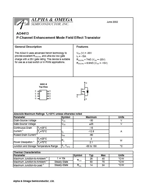
SymbolVDSVGSIDMTJ, TSTGSymbolTypMax7090100125RθJL6380WMaximum Junction-to-Lead CSteady-State°C/WThermal CharacteristicsParameterUnitsMaximum Junction-to-Ambient At ≤ 10sRθJA°C/WMaximum Junction-to-Ambient ASteady-State°C/W±8Gate-Source VoltageDrain-Source Voltage-20Continuous Drain Current AMaximumUnitsParameterTA=25°CTA=70°CAbsolute Maximum Ratings TA=25°C unless otherwise notedVV-2.4-15Pulsed Drain Current BPower Dissipation ATA=25°CJunction and Storage Temperature RangeAPD°C1.40.9-55 to 150TA=70°CID-3
AO3413P-Channel Enhancement Mode Field Effect Transistor
June 2003
FeaturesVDS (V) = -20VID = -3 ARDS(ON) < 97mΩ (VGS = -4.5V)RDS(ON) < 130mΩ (VGS = -2.5V)RDS(ON) < 190mΩ (VGS = -1.8V)General DescriptionThe AO3413 uses advanced trench technology to provide excellent RDS(ON), low gate charge and
operation with gate voltages as low as 1.8V. This device is suitable for use as a load switch or in PWM applications.
SGD
TO-236(SOT-23)Top View
G
D
S
Alpha & Omega Semiconductor, Ltd.AO3413SymbolMinTypMaxUnitsBVDSS-20V-1TJ=55°C-5IGSS±100nAVGS(th)-0.3-0.55-1VID(ON)-15A8197TJ=125°C111135108130mΩ146190mΩgFS47SVSD-0.78-1VIS-2ACiss540pFCoss72pFCrss49pFRg12ΩQg6.1nCQgs0.6nCQgd1.6nCtD(on)10nstr12nstD(off)44nstf22nstrr21nsQrr7.5nCGate resistanceVGS=0V, VDS=0V, f=1MHzTurn-Off Fall TimeMaximum Body-Diode Continuous CurrentInput CapacitanceOutput CapacitanceTurn-On DelayTimeDYNAMIC PARAMETERSIF=-3A, dI/dt=100A/µsVGS=0V, VDS=-10V, f=1MHzSWITCHING PARAMETERSTotal Gate ChargeVGS=-4.5V, VDS=-10V, ID=-3AGate Source ChargeGate Drain ChargeTurn-On Rise TimeTurn-Off DelayTimeVGS=-4.5V, VDS=-10V, RL=3.3Ω, RGEN=3ΩmΩVGS=-2.5V, ID=-2.6A IS=-1A,VGS=0VVDS=-5V, ID=-3ARDS(ON)Static Drain-Source On-ResistanceForward TransconductanceDiode Forward VoltageIDSSµAGate Threshold VoltageVDS=VGS ID=-250µAVDS=-16V, VGS=0V VDS=0V, VGS=±8VZero Gate Voltage Drain CurrentGate-Body leakage currentElectrical Characteristics (TJ=25°C unless otherwise noted)STATIC PARAMETERSParameterConditions
Body Diode Reverse Recovery TimeBody Diode Reverse Recovery ChargeIF=-3A, dI/dt=100A/µs
Drain-Source Breakdown VoltageOn state drain currentID=-250µA, VGS=0V VGS=-1.8V, ID=-1A VGS=-4.5V, VDS=-5VVGS=-4.5V, ID=-3A
Reverse Transfer Capacitance
A: The value of R θJA is measured with the device mounted on 1in 2 FR-4 board with 2oz. Copper, in a still air environment with T A =25°C. The value in any a given application depends on the user's specific board design. The current rating is based on the t ≤ 10s thermal resistance rating.B: Repetitive rating, pulse width limited by junction temperature.C. The R θJA is the sum of the thermal impedence from junction to lead R θJL and lead to ambient.D. The static characteristics in Figures 1 to 6,12,14 are obtained using 80 µs pulses, duty cycle 0.5% max.E. These tests are performed with the device mounted on 1 in 2 FR-4 board with 2oz. Copper, in a still air environment with T A=25°C. The SOA curve provides a single pulse rating.
Alpha & Omega Semiconductor, Ltd.AO3413TYPICAL ELECTRICAL AND THERMAL CHARACTERISTICS
051015
012345-VDS (Volts)Fig 1: On-Region Characteristics-ID (A)VGS=-1.5V-2.0V-2.5V-4.5V-8V-3.0V024600.511.52-VGS(Volts)
Figure 2: Transfer Characteristics
-ID(A)25°C125°C
VDS=-5V
501001502000246-ID (A)Figure 3: On-Resistance vs. Drain Current and Gate Voltage
RDS(ON) (mΩ)VGS=-1.8VVGS=-2.5VVGS=-4.5V
1E-061E-051E-041E-031E-021E-011E+001E+01
0.00.20.40.60.81.01.2-VSD (Volts)
Figure 6: Body-Diode Characteristics
-IS (A)25°C125°C0.811.21.41.61.80255075100125150175Temperature (°C)Figure 4: On-Resistance vs. Junction Temperature
Normalized On-ResistanceVGS=-2.5VVGS=-1.8VVGS=-4.5V
5010015020002468-VGS (Volts)Figure 5: On-Resistance vs. Gate-Source Voltage
RDS(ON) (mΩ)ID=-4A25°C125°C
Alpha & Omega Semiconductor, Ltd.