
SMX320C6201BW16中文资料
- 格式:pdf
- 大小:964.27 KB
- 文档页数:64

MBRS320
MBRS320, Rev. B2001 Fairchild Semiconductor Corporation
Features
•Compact surface mount with J-bend leads (SMC)
•3.0 Watt Power Dissipation package
•
3.0 Ampere, forward voltage less than 500 mVMBRS320
Schottky Rectifier
Absolute Maximum Ratings*
T
A = 25°C unless otherwise noted
Electrical Characteristics
T
A = 25°C unless otherwise noted
Symbol
Parameter
Value
Units
V
RRM Maximum Repetitive Reverse Voltage 20 V
I
F(AV) Average Rectified Forward Current
@ T
L = 100°C
T
L = 90°C 3.0
4.0 A
A
I
FSM Non-repetitive Peak Forward Surge Current
(Half wave, single phase, 60 Hz) 80 A
T
stg Storage Temperature Range -65 to +150 °C
T
j Operating Junction Temperature -65 to +125 °C
*These ratings are limiting values above which the serviceability of any semiconductor device may be impaired.
Symbol
Parameter
Value
Units
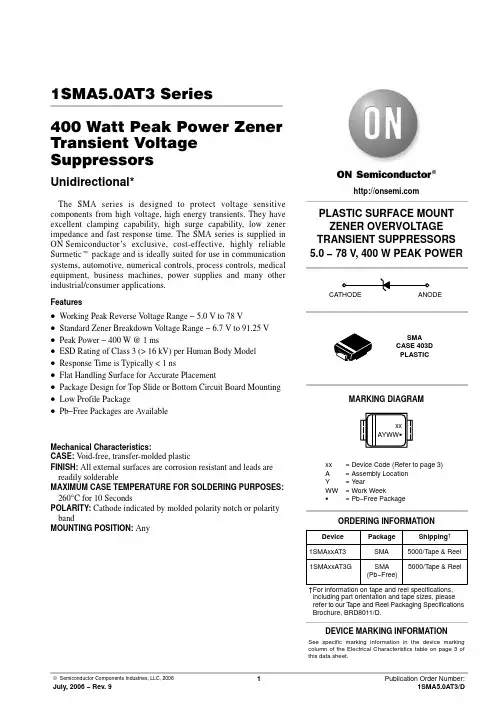
© Semiconductor Components Industries, LLC, 2006July, 2006 − Rev. 91Publication Order Number:1SMA5.0AT3/D1SMA5.0AT3 Series400 Watt Peak Power ZenerTransient VoltageSuppressorsUnidirectional*The SMA series is designed to protect voltage sensitivecomponents from high voltage, high energy transients. They haveexcellent clamping capability, high surge capability, low zenerimpedance and fast response time. The SMA series is supplied inON Semiconductor’s exclusive, cost-effective, highly reliableSurmetict package and is ideally suited for use in communicationsystems, automotive, numerical controls, process controls, medicalequipment, business machines, power supplies and many otherindustrial/consumer applications.Features•Working Peak Reverse Voltage Range − 5.0 V to 78 V•Standard Zener Breakdown Voltage Range − 6.7 V to 91.25 V•Peak Power − 400 W @ 1 ms•ESD Rating of Class 3 (> 16 kV) per Human Body Model•Response Time is Typically < 1 ns•Flat Handling Surface for Accurate Placement•Package Design for Top Slide or Bottom Circuit Board Mounting•Low Profile Package•Pb−Free Packages are AvailableMechanical Characteristics:CASE: Void-free, transfer-molded plasticFINISH: All external surfaces are corrosion resistant and leads arereadily solderableMAXIMUM CASE TEMPERATURE FOR SOLDERING PURPOSES:260°C for 10 SecondsPOLARITY: Cathode indicated by molded polarity notch or polaritybandMOUNTING POSITION: AnyPLASTIC SURFACE MOUNTZENER OVERVOLTAGETRANSIENT SUPPRESSORS5.0 − 78 V, 400 W PEAK POWER

系列 ■ 产品简介 系列是以CMOS工艺制造的高精度,低噪音,快速响应低压差线性稳压器。该系列的稳压器内置固定的参考电压,误差修正电路,限流电路,相位补偿电路以及低内阻的MOSFET,达到高纹波抑制,低输出噪音,快速响应低压差的性能。 系列兼容体积比钽电容更小的陶瓷电容,而且不需使用0.1μF的By-pass电容,更能节省空间,降低了成本。因具有高精度的输出稳定性,以及快速瞬态响应性能,从而能应付负载电流的波动,所以特别适合应用在手持设备及射频产品上。 通过控制芯片上的CE脚,可将输出关断,关断输出后的静态电流只有0.1uA(Typ值),从而大大降低了功耗。 ■ 产品特点 ■ 产品用途 ■ 封装形式和管脚定义功能
● 高精度输出电压:±2.0%; ● 可选择输出电压:1.8V~
5.0V
; ● 极低的静态电流(Typ.=15μA); ● 极低的关断电流(Typ.=0.1μA); ● 输入稳定性好:Typ.=0.2%/V; ● 智能手机/移动电话 ● 数码相机/摄像机 ● 电池供电设备 ● 带载能力强:当Vin=4.3V且Vout=3.3V时, Iout=300mA; ● 内置过流保护和负载短路保护; ● 兼容陶瓷电容; ● 封装形式:SOT89-5、SOT23-5 ● 蓝牙及其他射频产品 ● 便携式消费类设备 管脚序号 管脚 定义 功能说明 封装 SOT23-5 SOT89-5 1 4 VIN 输入端 2 2 VSS 接地端 3 3 CE 使能端 4 1 NC 空 5 5 VOUT 输出端 XC6219XC6219UMW RUMW XC6219
友台半导体有限公司XC6219
■ 功能框图
■ 极限参数
注:极限参数是指无论在任何条件下都不能超过的极限值。万一超过此极限值,将有可能造成产品劣化等物理性损伤;同时在接近极限参数下,不能全部保证芯片可以正常工作。 ■ 典型应用 项目 符号 说明 极限值 单位 电压 Vin 输入电压 9 V Vout 输出电压 Vss-0.3~Vin+0.3 V 电流 Iout 输出电流 500 mA 功耗 PD SOT23-5 最大允许功耗 200 mW SOT89-5 300 温度 TOPR 工作温度 -20~+60 ℃ Tstg 存储温度 -40~+125 ℃ Tsolder 焊接温度 260℃,10s

Rider 320⢪欽䩛ⱁ目錄
開始使用 ...............................
4
Rider 320
按鍵介紹 .......................... 4
配件................................................... 5
狀態圖示 ........................................... 5
步驟1:
充電您的 Rider 320 .............. 6
步驟2:
開啟您的Rider 320 .............. 6
步驟3:
初次設定 ............................... 6
步驟4:
接收衛星訊號 ........................ 7
步驟5:
使用Rider 320 ..................... 7
重新啟動Rider 320 .......................... 7
分享您的紀錄 .................................... 8
自動上傳紀錄至
Bryton Active App.............................. 9
下載Bryton Update Tool ................. 10
檢視歷史紀錄 ..................... 11
檢視運動/訓練紀錄 ..................... 11
刪除歷史紀錄 ............................... 11
歷史紀錄...................................... 12
設定 .................................. 13
碼錶資訊 ......................................... 13