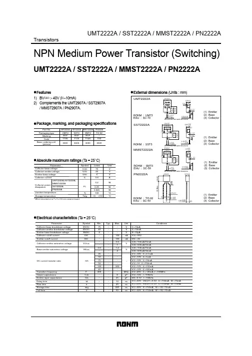
SM8122AWhite LED Driver ICOVERVIEWThe SM8122A is a high efficiency step-up DC/DC converter. Due to high voltage CMOS process realizing 25V output supply as maximum value, 2 to 6 lights of white LED connected in series can be lighted. By con-necting in series, current variation among LED is eliminated. Current value sent to white LED can be set by external resistors. In addition, brightness can also be adjusted by control to FB pin or CE pin. Since the SM8122A has an over voltage protection circuit built-in, it dispenses with the existing external ZD (zener diode). Besides, the switching frequency of the SM8122A is higher (2.0MHz) than the existing product (SM8121A), so that it can respond to lower inductance value.FEATURESI Boost-up control using PWMI 2 to 6 lights of white L ED (connected in series) lightedI Output current value can be set by external resis-tors (51Ω: 9.8mA, 33Ω: 15.2mA, 24Ω: 20.8mA) I Brightness adjustable by control to FB pin or CE pinI Current variation among LED decreased by high precisionI High efficient drive by step-up modelI Over voltage protection circuit built-inI Supply voltage range: 2.3 to 5.5VI Maximum output voltage: 25VI Quiescent current: 820µA (typ)I Standby current: 1.0µA (max)I R ON (Switching MOS-Tr): 2Ω (typ)I Switching frequency: 2.0MHz (typ)I Output current detection accuracy: ± 2%I Package: SOT23-6W (SM8122AH)MSON-6 (SM8122AD) APPLICATIONSI Cellular phoneI PagerI Digital still cameraI Handy terminalI PDAsI Portable gamesI White LED driveI LCD bias supplyI Flash memory supplyORDERING INFORMATION PINOUT (Top view)I SOT23-6W I MSON-6Device Package SM8122AH SOT23-6W SM8122AD MSON-6SWVOUTFB123VDDCE64VSS56431CESWVDD2VOUT5VSSFB元器件交易网SM8122APACKAGE DIMENSIONS(Unit: mm)ISOT23-6WIMSON-6+ 0.1元器件交易网SM8122ABLOCK DIAGRAMPIN DESCRIPTIONNumberName I/O DescriptionSOT23-6WMSON-6 12SW O Coil switching 26VOUT I Output voltage detection34FB I Feed back (Output current detection)43CE Ip 11.Input with built-in pull-down resistorChip enable (High active)55VSS –GND 61VDD–Power supplyCEVDDFB元器件交易网SM8122ASPECIFICATIONSAbsolute Maximum RatingsElectrical CharacteristicsV DD = 3.6V , V SS = 0V , Ta = 25 ° C unless otherwise notedParameterSymbol Rating Unit Supply voltage range V DD − 0.3 to 6.5V Input voltage range V IN V SS – 0.3 to V DD + 0.3V SW output voltage range V SW –0.3 to 30V SW input current I SW 500mA Power dissipationP D 250 (Ta = 25 ° C)mW Operating temperature range T opr –40 to 85 ° C Storage temperature rangeT stg− 55 to 125° CParameterPin Symbol ConditionRatingUnit min typ max Supply voltage VDD V DD 2.3 3.6 5.5V Maximum output voltage SW V OUT ––25V Standby current VDD I STB V CE = 0V –– 1.0 µ A Quiescent current VDD I DD V FB = 1.0V –200400 µ A V FB = 0V–8201600 µ A SW-Tr ON resister SW R ON I SW = 100mA, V DD = 3.6V – 2.0 3.0 Ω SW-Tr leak current SW I LEAK V SW = V DD –– 1.0 µ A Switching frequency SW f OSC V FB = 0V 1.8 2.0 2.2MHz Maximum duty SW Duty V FB = 0V758590%Input voltageCE V IH 2.0––V V IL ––0.6V Input currentCEI CE V CE = 3.6V – 5.010 µ A FB I FB V FB = 0.5V –1.0– 1.0 µ A VOUTI VOUT V OUT = 25V 6082120 µ A Soft-start time SW T SS1 Switching stop time 102070 µ s T SS2 Maximum duty restriction time –500– µ s FB voltage FB V FB 0.490.500.51V Coil inductance SW L SW – 4.710 µ H Over voltage detection VOUTV OV 2530.536V Over voltage detection releaseV OVR2328.5–V元器件交易网SM8122AOPERATION OVERVIEWThe SM8122A basic structure is a step-up DC/DC converter. The booster control employs Pulse Width Modu-lation (PWM) which controls the pulse duty cycle (85% max.) at constant frequency (2.0MHz typ.). The LED current is set by a current-setting resistor R1 connected between pins FB (with stable voltage of 0.5V typ.) and VSS.When the switching transistor SW-Tr is ON, energy is stored in the inductor L. When SW-Tr is rapidly switched OFF, the energy stored in the inductor generates a voltage across the terminals of the inductor. The induced voltage, after being added to the input voltage, turns ON the Schottky barrier diode SBD and the stored energy is transferred to the output capacitor. This sequence of events continues repeatedly, boosting the output voltage.The SM8122A features a built-in soft-start function. The soft-start time is approximately 500 µs from after the chip enable input CE rising edge. During this interval, the maximum duty is restricted.L C V INOUT µF元器件交易网SM8122AOVP (Over Voltage Protection)SM8122A is always monitoring the VOUT terminal voltage in order to protect itself from the stress of V OUT over voltage. If SM8122A detects the V OUT over voltage, it immediately stop the switching of the inductor drive transistor. After the VOUT terminal voltage decreases below the release voltage, SM8122A restarts switching the inductor drive transistor. The over voltage is set as approximately 30.5V , the release voltage is approximately 28.5V .Selecting the Current-setting Resistor (R1)The SM8122A control stabilizes the voltage on pin FB (0.5V typ.). Hence, the current-setting resistor R1 con-nected between FB and VSS sets the LED current I LED , where the resistance R1 is given by the following equation.R1 = 0.5 / ILED30.5V28.5VV O U TLED =0.5/R1元器件交易网SM8122ASelecting the Inductor (L)The inductor DC resistance affects the power efficiency, therefore a low DC resistance inductor is recom-mended. Note also that the peak inductor current I peak should not exceed the inductor maximum current rating. In pulsed current mode control, the peak inductor current I peak is given by the following equation.I peak = (V IN× T ON) / LFor example, if the input voltage V IN is 3.6V, the inductance L is 4.7µH, and the SW-Tr ON time T ON is 2MHz × 85% = 0.425µs, then the peak inductor current I peak is (3.6 × 0.425 × 10-6) / (4.7 × 10⁻⁶) = 0.326A = 326mA. Selecting the Capacitors (C IN, C OUT)The recommended capacitances for use with the SM8122A are 4.7µF ceramic input capacitor C IN and 1.0µF ceramic output capacitor C OUT. The capacitor ESR ratings affect the ripple voltage, therefore capacitors with low ESR rating are recommended. The input capacitor should be mounted close to the SM8122A IC. Note that the capacitor voltage ratings should be selected to provide sufficient margin for the applied input and output voltages.For example, if a lithium-ion battery (2.5 to 4.5V) is connected to the input and 3 white LEDs connected in series at the output draw 20mA, then the maximum input voltage is 4.5V and the maximum output voltage is (4.0V × 3 LEDs) + 0.5V = 12.5V. Therefore, the input capacitor should have a voltage rating of 6V, and the output capacitor should have a voltage rating of 16V.Selecting the Rectifier Schottky Barrier Diode (SBD)The rectifier schottky barrier diode forward-direction voltage drop affects the power efficiency, therefore a Schottky barrier diode with low forward-direction voltage drop is recommended. Note that the diode should be selected to provide sufficient margin for the rated current and reverse-direction withstand voltage.Board Layout NotesThe following precautions should be followed for stable device operation.I The inductor L and Schottky barrier diode SBD should be connected close to the pin SW using thick, short circuit wiring.I The input capacitor C IN should be mounted close to the IC.I The IC supply voltage V DD wiring and inductor supply wiring should be isolated, reducing any common impedances.I The ground wiring should be connected at a single point, reducing any common impedances.V IN LED元器件交易网BRIGHTNESS ADJUSTMENT Brightness Adjustment using FB PinThe LED brightness can be adjusted using an input DC control voltage connected through resistor R3 to the FB pin. Alternatively, the brightness can be controlled by a PWM signal by adding a low-pass filter comprising resistor R4 and capacitor C1. The PWM signal frequency range is determined by the low-pass filter coeffi-cients. For example, the recommended values for resistor R4 (50k Ω) and capacitor C1 (0.1µF) provide a PWM signal frequency range of 1kHz to 1MHz.Brightness adjustment using FB pin (DC voltage input)When the brightness is controlled by DC voltage (V DC ) connected to resistor R3, the LED current (I LED ) is given by equation 1.If the values R1 = 30Ω, R2 = 20k Ω, R3 = 100k Ω, V FB = 0.5V , and V DC = 0V are inserted in equation 1, the LED current I LED = 20mA, as shown in equation 2.If the values R1 = 30Ω, R2 = 20k Ω, R3 = 100k Ω, V FB = 0.5V , and V DC = 3V are inserted in equation 1, the LED current I LED = 0mA, as shown in equation 3.Taking the above diagram as an example, inserting the values R1 = 30Ω, R2 = 20k Ω, R3 = 100k Ω, V FB = 0.5V ,and V DC = 0 to 3V into equation 1 gives the maximum LED current I LED of 20mA when V DC = 0V (equation 2) and the minimum LED current I LED of 0mA when V DC = 3V (equation 3).Brightness adjustment circuit using FB pin(DC voltage input)ΩV DC voltage vs. LED current051015200.00.51.01.52.02.53.0DC voltage [V]L E D c u r r e n t [m A ]R1R2 × (V DC − V FB )R3I LED =V FB − (1)20,000 × (0 − 0.5)100,0003030I LED===0.5 −0.620mA (2)20,000 × (3 − 0.5)100,0003030I LED===0.5 −0mA (3)Brightness adjustment using FB pin (PWM signal input)When the brightness is controlled by PWM signal (V PWM × Duty), the LED current (I LED ) is given by equa-tion 4.If the values R1 = 30Ω, R2 = 20k Ω, R3 = 50k Ω, R4 = 50k Ω, V FB = 0.5V , V PWM = 3V , and Duty = 0% are inserted in equation 4, the LED current I LED = 20mA, as shown in equation 5.If the values R1 = 30Ω, R2 = 20k Ω, R3 = 50k Ω, R4 = 50k Ω, V FB = 0.5V , V PWM = 3V , and Duty = 100% are inserted in equation 4, the LED current I LED = 0mA, as shown in equation 6.Taking the above diagram as an example, inserting the values R1 = 30Ω, R2 = 20k Ω, R3 = 50k Ω, R4 = 50k Ω,V FB = 0.5V , V PWM = 3V , and Duty = 0 to 100% into equation 4 gives the maximum LED current I LED of 20mA when Duty = 0% (equation 5) and the minimum LED current I LED of 0mA when Duty = 100% (equa-tion 6).Brightness adjustment circuit using FB pin(PWM signal input)ΩV PWM signal vs. LED current051015200.00.51.01.52.02.53.0V PWM × Duty [V]L E D c u r r e n t [m A ]R2 × (V PWM × Duty − V FB )R3 +R4R1I LED =V FB − (4)3030I LED ===20,000 × (3 × 0 − 0.5)50,000 + 50,0000.5 −0.620mA (5)3030I LED ===20,000 × (3 × 1 − 0.5)50,000 + 50,0000.5 −0mA (6)Brightness Adjustment using CE PinThe LED average current can be adjusted by controlling the duty of a PWM signal input on the CE pin. When CE goes from LOW to HIGH, the soft start function operates (with 500µs constant soft start time) and, there-fore, the LED average current ratio for a given PWM signal duty falls with increasing PWM signal frequency.Taking this into consideration, the recommended PWM control signal has a frequency range of 100 to 400Hz with duty cycle range of 10 to 90%.When adjusting the brightness using the CE pin, a ripple voltage synchronized to the PWM signal is generated across the output capacitor C OUT . The amplitude of the ripple voltage is determined by the number of LEDs and their forward-bias voltage drop characteristics. If a ceramic capacitor is used for the output capacitor C OUT , an audible noise may be generated due to the ceramic capacitor ’s piezoelectric effect. The audible noise level depends on the ceramic capacitor (capacitance, bias dependency, withstand voltage etc.), LEDs (number,forward-bias voltage drop etc.), and mounting board (thickness, mounting conditions etc.), and thus should be veri fied under actual conditions.Brightness adjustment circuit using CE pinΩVPWM signal duty vs. LED average current10200.05.010.015.020.0030405060708090100PWM signal duty [%]A v e r a g e L E D c u r r e n t [mA ]Alternatively, a tantalum capacitor or film capacitor with low piezoelectric effect can be used as the output capacitor C OUT to minimize the noise level, or the brightness can be adjusted using the FB pin as described earlier. The audible noise generated when using the CE pin is not an inherent phenomena of the SM8122A device, but of the brightness adjustment method employed.Output voltage with LEDs ONOutput voltage with LEDsOFFCE input signal and output ripple voltageCurrent Switching using External TransistorsIf only a few brightness steps are required, the LED current can be adjusted by switching the LED current set-ting resistance using external transistors (Tr).ΩV Select signal 2Select signal 1I LEDLow Low 2mALow High 2 + 5 = 7mA HighLow 2 + 12.5 = 14.5mA HighHigh2 + 5 + 12.5 = 19.5mARECOMMEND PATTERN SOT23-6WMSON-6Footprint pattern1.Footprint patternçMetalmask patternNC0323AE2005.05。