ADV7393应用电路
- 格式:pdf
- 大小:331.57 KB
- 文档页数:3
Rev.0“Circuits from the Lab” from Analog Devices have been designed and built by Analog Devices engineers. Standard engineering practices have been employed in the design and construction of each circuit, and their function and performance have been tested and verified in a labenvironment at room temperature. However, you are solely responsible for testing the circuit and determining its suitability and applicability for your use and application. Accordingly, in no event shall Analog Devices be liable for direct, indirect, special, incidental, consequential or One Technology Way, P.O. Box 9106, Norwood, MA 02062-9106, U.S.A. Tel: 电路笔记CN-0101连接/参考器件利用ADI公司产品进行电路设计低成本、高速、轨到轨输出视频滤波器ADA4430-1放心运用这些配套产品迅速完成设计。
欲获得更多信息和/或技术支持,请拨打4006-100-006或访问10位、2倍过采样标清电视视频编码器/zh/circuits。
ADV7393在视频编码器ADV7393之后采用放大器ADA4430-1的重构视频滤波器ADA4430-1是一款单通道、六阶、低通视频滤波器,−3 dB截止频率为9 MHz,27 MHz时的带外抑制为50 dB。
该器件为低功耗、低成本、轨到轨输出放大器,采用+2.5 V至+6 V电源供电,非常适合SD视频应用。
配合单芯片视频编码器ADV7393使用时,ADA4430-1能针对汽车应用提供功效比最高的视频输出解决方案。
电路功能与优势本电路由一个数模视频转换器与一个低成本、低功耗、全集成式重构视频滤波器配合组成。
虽然ADV7393等许多视频编码器(视频DAC)可以直接驱动视频负载,但在视频编码器的输出端使用视频驱动器往往非常有利,可以节省功耗,实现线路驱动,并提供更好的电路保护。
该视频驱动器通常配置为有源滤波器,也称为重构滤波器或抗镜像滤波器。
重构滤波器的作用有两方面:阻隔数字化处理过程中引入视频信号的较高频率部分(高于奈奎斯特频率),此外还提供增益,以驱动与视频显示器相连的75 Ω外部电缆。
对于交流耦合输出应用,ADA4430-1集成了信号振幅增益(SAG)校正网络。
后部端接电缆的150 Ω负载电阻与输出耦合电容构成一个高通滤波器,利用SAG校正可为该高通滤波器提供低频补偿。
SAG校正可以降低传统的大交流耦合电容(330 μF)要求,而用较小的47 μF和22 μF电容取而代之。
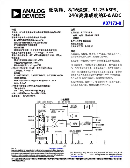
图1中,ADA4430-1配置为重构视频滤波器,提供交流耦合输出和SAG校正。
补偿网络包括C1、C2以及ADA4430-1中集成的内部电阻网络。
传统交流耦合采用昂贵的大耦合电容,不仅成本高,而且浪费宝贵的PCB空间。
SAG校正可以用两个较小的低成本电容取代一个较大的交流耦合电容,同时保持同样的场倾斜。
场倾斜是对交流耦合电容施加恒定的亮度信号时,所产生电压降(倾斜)的量度。
该电压降由75 Ω负载电阻产生的小放电电流引起。
选择适当的SAG校正电容值,便可实现与220 μF交流耦合电容相当的场倾斜。
使用SAG校正电路时,从ADA4430-1的输入端到最近输出端的增益在极低频率时为2.5 (≈8 dB)。
这种情况下,由22 μF电容构成的外反馈环路会有效打开(参见ADA4430-1和ADV7393均推荐用于汽车领域,非常适合信息娱乐系统及基于视觉的安全系统。
图2),并在约5 Hz时表现出大约11 dB的二阶峰值。
此增益在30 Hz时大约为7.5dB。
在考虑低频输入和输出信号摆幅时,必须注意该额外增益,使这些摆幅保持在额定限值内。
从ADA4430-1输入端到47 μF电容负载端的增益没有表现出这种行为;相反,它更像是单极高通响应。
电路描述ADV7393是一款低功耗、全集成式数字视频编码器,可将CMOS后视摄像头之类的16位数字分量视频数据转换为与全球标准兼容的标准模拟基带视频信号。
三个2.6 V/3.46 V 10位视频DAC支持标清(SD)或高清(HD)视频格式的复合(CVBS)、S视频(YC)或分量(YPrPb/RGB)模拟输出。
图1所示电路配置为低输出驱动工作模式,可将所有三个DAC的输出电流降低85%(R SET = 4.12 kΩ,R L = 300 Ω)。
为进一步节省功耗,可以禁用内部PLL,并让编码器以2×过采样模式工作。
16位视频输入端口经过配置可支持标清视频。
CN-0101 电路笔记图1.使用ADA4430-1的低成本、全集成式重构滤波器(原理示意图)电路笔记CN-0101(Continued from first page) "Circuits from the Lab" are intended only for use with Analog Devices products and are the intellectual property of Analog Devices or its licensors. While you may use the "Circuits from the Lab" in the design of your product, no other license is granted by implication or otherwise under any patents or other intellectual property by application or use of the "Circuits from the Lab". Information furnished by Analog Devices is believed to be accurate and reliable. However, "Circuits from the Lab" are supplied "as is" and without warranties of any kind, express, implied, or statutory including, but not limited to, any implied warranty of merchantability, noninfringement or fitness for a particular purpose and no responsibility is assumed by Analog Devices for their use, nor for any infringements of patents or other rights of third parties that may result from their use. Analog Devices reserves the right to change any "Circuits from the Lab" at any time without notice, but is under no obligation to do so. Trademarks and registered trademarks are the property of their respective owners.©2009 Analo 进一步阅读图2显示紧邻ADA4430-1输出端以及47μF 电容负载端的SAG 频率响应。
Kester, Walt. 2005. The Data Conversion Handbook . Analog Devices. Chapters 8 and 9.MT-031 Tutorial, Grounding Data Converters and Solving the Mystery of AGND and DGND . Analog Devices.MT-101 Tutorial, Decoupling Techniques . Analog Devices.数据手册和评估板ADA4430-1 Data Sheet.ADV7393 Data Sheet.修订历史7/09—Revision 0: Initial Version图2. ADA4430-1输出端以及47 μF 电容负载端的SAG 校正频率响应缓冲功能非常重要,却经常被忽视。
例如,许多汽车应用客户会采用低成本放大器来保护昂贵而复杂的器件,如视频解码器和编码器等。
带有交流耦合输出端的放大器,如图1所示,有助于保护这些器件免受过压和ESD 损坏。
常见变化图1交流耦合输出配置有多种选择。
所示的SAG 校正采用22 μF 和47 μF 电容。
传统的交流耦合输出使用一个220 μF 电容;在这种配置中,SAG 引脚直接与输出电容之前的输出引脚相连。
对于直流耦合配置,SAG 引脚也直接与输出引脚相连。
在直流耦合配置和传统的交流耦合配置中,将SAG 引脚直接与输出引脚相连可在所有视频频率产生+2的增益缓冲。
g Devices, Inc. All rights reserved. Trademarks and registered trademarks are the property of their respective owners.CN08373-0-7/09(0)w w w .a n a l o g .c o m。