
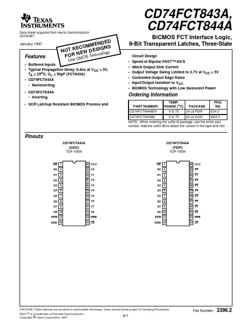
CD74FCT843A(844A)
- 格式:pdf
- 大小:33.21 KB
- 文档页数:6

SN74CBT3306CDUAL FET BUS SWITCH5ĆV BUS SWITCH WITH ć2ĆV UNDERSHOOT PROTECTIONSCDS127A − SEPTEMBER 2003 − REVISED OCTOBER 2003D Undershoot Protection for Off-Isolation on A and B Ports Up To −2 VD Bidirectional Data Flow, With Near-Zero Propagation DelayD Low ON-State Resistance (r on )Characteristics (r on = 3 Ω Typical)D Low Input/Output Capacitance Minimizes Loading and Signal Distortion (C io(OFF) = 5 pF Typical)D Data and Control Inputs Provide Undershoot Clamp Diodes D Low Power Consumption (I CC = 3 µA Max)D V CC Operating Range From 4 V to 5.5 V DData I/Os Support 0 to 5-V Signaling Levels (0.8-V, 1.2-V, 1.5-V, 1.8-V, 2.5-V, 3.3-V, 5-V)D Control Inputs Can Be Driven by TTL or 5-V/3.3-V CMOS OutputsD I off Supports Partial-Power-Down Mode OperationD Latch-Up Performance Exceeds 100 mA Per JESD 78, Class IIDESD Performance Tested Per JESD 22− 2000-V Human-Body Model (A114-B, Class II)− 1000-V Charged-Device Model (C101)DSupports Both Digital and AnalogApplications: USB Interface, Bus Isolation,Low-Distortion Signal GatingD OR PW PACKAGE(TOP VIEW)123487651OE 1A 1B GNDV CC 2OE 2B 2Adescription/ordering informationThe SN74CBT3306C is a high-speed TTL-compatible FET bus switch with low ON-state resistance (r on ),allowing for minimal propagation delay. Active Undershoot-Protection Circuitry on the A and B ports of the SN74CBT3306C provides protection for undershoot up to −2 V by sensing an undershoot event and ensuring that the switch remains in the proper OFF state.The SN74CBT3306C is organized as two 1-bit bus switches with separate output-enable (1OE, 2OE) inputs.It can be used as two 1-bit bus switches or as one 2-bit bus switch. When OE is low, the associated 1-bit bus switch is ON, and the A port is connected to the B port, allowing bidirectional data flow between ports. When OE is high, the associated 1-bit bus switch is OFF, and the high-impedance state exists between the A and B ports.ORDERING INFORMATIONT APACKAGE †ORDERABLE PART NUMBER TOP-SIDE MARKING Tube SN74CBT3306CD SOIC − DTape and reel SN74CBT3306CDR CU306C −40°C to 85°CTube SN74CBT3306CPW TSSOP − PWTape and reelSN74CBT3306CPWRCU306C†Package drawings, standard packing quantities, thermal data, symbolization, and PCB design guidelines are available at /sc/package.Copyright 2003, Texas Instruments IncorporatedPlease be aware that an important notice concerning availability, standard warranty, and use in critical applications of Texas Instruments semiconductor products and disclaimers thereto appears at the end of this data sheet.PRODUCTION DATA information is current as of publication date.SN74CBT3306CDUAL FET BUS SWITCH5ĆV BUS SWITCH WITH ć2ĆV UNDERSHOOT PROTECTIONSCDS127A − SEPTEMBER 2003 − REVISED OCTOBER 2003description/ordering information (continued)This device is fully specified for partial-power-down applications using I off . The I off feature ensures that damaging current will not backflow through the device when it is powered down. The device has isolation during power off.To ensure the high-impedance state during power up or power down, OE should be tied to V CC through a pullup resistor; the minimum value of the resistor is determined by the current-sinking capability of the driver.FUNCTION TABLE (each bus switch)INPUT INPUT/OUTPUTOE AFUNCTION L B A port = B port HZDisconnectlogic diagram (positive logic)1A 1OESW1B2A 2OESW2B215736simplified schematic, each FET switch (SW)AEN †B†EN is the internal enable signal applied to the switch.Undershoot Protection CircuitSN74CBT3306CDUAL FET BUS SWITCH5ĆV BUS SWITCH WITH ć2ĆV UNDERSHOOT PROTECTIONSCDS127A − SEPTEMBER 2003 − REVISED OCTOBER 2003 absolute maximum ratings over operating free-air temperature range (unless otherwise noted)†. . . . . . . . . . . . . . . . . . . . . . . . . . . . . . . . . . . . . . . . . . . . . . . . . . . . . . . . . .Supply voltage range, V CC−0.5 V to 7 V Control input voltage range, V IN (see Notes 1 and 2) −0.5 V to 7 V. . . . . . . . . . . . . . . . . . . . . . . . . . . . . . . . . . .. . . . . . . . . . . . . . . . . . . . . . . . . . . . . . . . . .Switch I/O voltage range, V I/O (see Notes 1, 2, and 3) −0.5 V to 7 V. . . . . . . . . . . . . . . . . . . . . . . . . . . . . . . . . . . . . . . . . . . . . . . . . . .Control input clamp current, I IK(V IN< 0) −50 mA. . . . . . . . . . . . . . . . . . . . . . . . . . . . . . . . . . . . . . . . . . . . . . . . . . . . .I/O port clamp current, I I/OK(V I/O< 0) −50 mA ON-state switch current, I I/O (see Note 4) ±128 mA. . . . . . . . . . . . . . . . . . . . . . . . . . . . . . . . . . . . . . . . . . . . . . . . .. . . . . . . . . . . . . . . . . . . . . . . . . . . . . . . . . . . . . . . . .Continuous current through V CC or GND terminals ±100 mA. . . . . . . . . . . . . . . . . . . . . . . . . . . . . . . . . . .Package thermal impedance, θJA (see Note 5):D package 97°C/W. . . . . . . . . . . . . . . . . . . . . . . . . . . . . . . .PW package 149°C/W Storage temperature range, T stg −65°C to 150°C. . . . . . . . . . . . . . . . . . . . . . . . . . . . . . . . . . . . . . . . . . . . . . . . . . .†Stresses beyond those listed under “absolute maximum ratings” may cause permanent damage to the device. These are stress ratings only, and functional operation of the device at these or any other conditions beyond those indicated under “recommended operating conditions” is not implied. Exposure to absolute-maximum-rated conditions for extended periods may affect device reliability.NOTES: 1.All voltages are with respect to ground unless otherwise specified.2.The input and output voltage ratings may be exceeded if the input and output clamp-current ratings are observed.3.V I and V O are used to denote specific conditions for V I/O.4.I I and I O are used to denote specific conditions for I I/O.5.The package thermal impedance is calculated in accordance with JESD 51-7.recommended operating conditions (see Note 6)MIN MAX UNITV CC Supply voltage4 5.5VV IH High-level control input voltage2 5.5VV IL Low-level control input voltage00.8VV I/O Data input/output voltage0 5.5VT A Operating free-air temperature−4085°C NOTE 6:All unused control inputs of the device must be held at V CC or GND to ensure proper device operation. Refer to the TI application report, Implications of Slow or Floating CMOS Inputs, literature number SCBA004.SN74CBT3306CDUAL FET BUS SWITCH5ĆV BUS SWITCH WITH ć2ĆV UNDERSHOOT PROTECTIONSCDS127A − SEPTEMBER 2003 − REVISED OCTOBER 2003electrical characteristics over recommended operating free-air temperature range (unless otherwise noted)PARAMETER TEST CONDITIONS MINTYP †MAX UNIT V IK Control inputs V CC = 4.5 V,I IN = −18 mA−1.8V V IKU Data inputs V CC = 5 V,0 mA > I I ≥ −50 mA,V IN = V CC or GND,Switch OFF−2V I IN Control inputsV CC = 5.5 V,V IN = V CC or GND ±1µA I OZ ‡V CC = 5.5 V,V O = 0 to 5.5 V,V I = 0,Switch OFF,V IN = V CC or GND ±10µA I off V CC = 0,V O = 0 to 5.5 V,V I = 010µA I CC V CC = 5.5 V,I I/O = 0,V IN = V CC or GND,Switch ON or OFF3µA ∆I CC §Control inputs V CC = 5.5 V,One input at 3.4 V,Other inputs at V CC or GND2.5mA C in Control inputs V IN = 3 V or 0 3.5pF C io(OFF)V I/O = 3 V or 0,Switch OFF,V IN = V CC or GND 5pF C io(ON)V I/O = 3 V or 0,Switch ON,V IN = V CC or GND 12.5pFV CC = 4 V,TYP at V CC = 4 VV I = 2.4 V,I O = −15 mA 812on ¶V I O = 64 mA 36r V I = 0I O = 30 mA36ΩCC = 4.5 VV I = 2.4 V,I O = −15 mA 510V IN and I IN refer to control inputs. V I , V O , I I , and I O refer to data pins.†All typical values are at V CC = 5 V (unless otherwise noted), T A = 25°C.‡For I/O ports, the parameter I OZ includes the input leakage current.§This is the increase in supply current for each input that is at the specified voltage level, rather than V CC or GND.¶Measured by the voltage drop between the A and B terminals at the indicated current through the switch. ON-state resistance is determined by the lower of the voltages of the two (A or B) terminals.switching characteristics over recommended operating free-air temperature range (unless otherwise noted) (see Figure 3)FROM TO V CC = 4 V V CC = 5 V ± 0.5 V PARAMETER(INPUT)(OUTPUT)MINMAX MINMAX UNITt pd # A or B B or A 0.240.15ns t en OE A or B 4.6 1.5 4.2ns t disOEA or B4.31.5 4.3ns #The propagation delay is the calculated RC time constant of the typical ON-state resistance of the switch and the specified load capacitance,when driven by an ideal voltage source (zero output impedance).SN74CBT3306CDUAL FET BUS SWITCH5ĆV BUS SWITCH WITH ć2ĆV UNDERSHOOT PROTECTIONSCDS127A − SEPTEMBER 2003 − REVISED OCTOBER 2003undershoot characteristics (see Figures 1 and 2)PARAMETERTEST CONDITIONSMIN TYP †MAXUNIT V OUTU V CC = 5.5 V,Switch OFF,V IN = V CC or GND2V OH −0.3V†All typical values are at V CC = 5 V (unless otherwise noted), T A = 25°C.Figure 1. Device Test Setup50 ΩV SV CC11 V 100 k Ω100 k Ω10 pFDUTInputGeneratorAxBxFigure 2. Transient Input Voltage (V I ) and OutputVoltage (V OUTU ) Waveforms(Switch OFF)−2 V5.5 V10 %20 ns10 %90 %90 %2 ns2 nsV OH − 0.3V OHOutput (V OUTU )Input (Open Socket)SN74CBT3306CDUAL FET BUS SWITCH5ĆV BUS SWITCH WITH ć2ĆV UNDERSHOOT PROTECTIONSCDS127A − SEPTEMBER 2003 − REVISED OCTOBER 2003PARAMETER MEASUREMENT INFORMATIONV OH V OLC L(see Note A)TEST CIRCUITS17 VOpen GNDR LR Lt PLH t PHLOutput Waveform 1S1 at 7 V (see Note B)Output Waveform 2S1 at Open (see Note B)t PZLt PZHt PLZt PHZ 3 V0 V V OH V OL0 VV OL + V ∆V OH − V ∆0 VOutput Control (V IN )3 V3.5 VVOLTAGE WAVEFORMSPROPAGATION DELAY TIMES (t pd(s))VOLTAGE WAVEFORMS ENABLE AND DISABLE TIMESOutputNOTES: A.C L includes probe and jig capacitance.B.Waveform 1 is for an output with internal conditions such that the output is low except when disabled by the output control.Waveform 2 is for an output with internal conditions such that the output is high except when disabled by the output control.C.All input pulses are supplied by generators having the following characteristics: PRR ≤10 MHz, Z O = 50 Ω, t r ≤2.5 ns, t f ≤2.5 ns.D.The outputs are measured one at a time with one transition per measurement.E.t PLZ and t PHZ are the same as t dis .F.t PZL and t PZH are the same as t en .G.t PLH and t PHL are the same as t pd(s). The tpd propagation delay is the calculated RC time constant of the typical ON-stateresistance of the switch and the specified load capacitance, when driven by an ideal voltage source (zero output impedance).H.All parameters and waveforms are not applicable to all devices.1.5 V1.5 V1.5 V1.5 V1.5 V 1.5 V1.5 V1.5 V50 ΩV G1V CCDUT50 ΩV IN50 ΩV G250 ΩV ITEST R L S1V ∆C L 5 V ±0.5 V4 V V CC V I t PHZ /t PZHt PLZ /t PZL t pd(s) 5 V ±0.5 V4 V5 V ±0.5 V4 VOpen Open 7 V 7 V Open Open500 Ω500 Ω500 Ω500 Ω500 Ω500 ΩV CC or GND V CC or GNDGND GND V CC V CC 50 pF 50 pF 50 pF 50 pF 50 pF 50 pF0.3 V 0.3 V 0.3 V 0.3 VOutput Control (V IN )Input GeneratorInput GeneratorV OFigure 3. Test Circuit and Voltage WaveformsPACKAGING INFORMATION(1) The marketing status values are defined as follows:ACTIVE: Product device recommended for new designs.LIFEBUY: TI has announced that the device will be discontinued, and a lifetime-buy period is in effect.NRND: Not recommended for new designs. Device is in production to support existing customers, but TI does not recommend using this part in a new design.PREVIEW: Device has been announced but is not in production. Samples may or may not be available.OBSOLETE: TI has discontinued the production of the device.(2) RoHS: TI defines "RoHS" to mean semiconductor products that are compliant with the current EU RoHS requirements for all 10 RoHS substances, including the requirement that RoHS substance do not exceed 0.1% by weight in homogeneous materials. Where designed to be soldered at high temperatures, "RoHS" products are suitable for use in specified lead-free processes. TI may reference these types of products as "Pb-Free".RoHS Exempt: TI defines "RoHS Exempt" to mean products that contain lead but are compliant with EU RoHS pursuant to a specific EU RoHS exemption.Green: TI defines "Green" to mean the content of Chlorine (Cl) and Bromine (Br) based flame retardants meet JS709B low halogen requirements of <=1000ppm threshold. Antimony trioxide based flame retardants must also meet the <=1000ppm threshold requirement.(3) MSL, Peak Temp. - The Moisture Sensitivity Level rating according to the JEDEC industry standard classifications, and peak solder temperature.(4) There may be additional marking, which relates to the logo, the lot trace code information, or the environmental category on the device.(5) Multiple Device Markings will be inside parentheses. Only one Device Marking contained in parentheses and separated by a "~" will appear on a device. If a line is indented then it is a continuation of the previous line and the two combined represent the entire Device Marking for that device.(6) Lead finish/Ball material - Orderable Devices may have multiple material finish options. Finish options are separated by a vertical ruled line. Lead finish/Ball material values may wrap to two lines if the finish value exceeds the maximum column width.Important Information and Disclaimer:The information provided on this page represents TI's knowledge and belief as of the date that it is provided. TI bases its knowledge and belief on information provided by third parties, and makes no representation or warranty as to the accuracy of such information. Efforts are underway to better integrate information from third parties. TI has taken andAddendum-Page 1continues to take reasonable steps to provide representative and accurate information but may not have conducted destructive testing or chemical analysis on incoming materials and chemicals. TI and TI suppliers consider certain information to be proprietary, and thus CAS numbers and other limited information may not be available for release.In no event shall TI's liability arising out of such information exceed the total purchase price of the TI part(s) at issue in this document sold by TI to Customer on an annual basis.Addendum-Page 2TAPE AND REEL INFORMATION*All dimensions are nominalDevicePackage Type Package Drawing Pins SPQReel Diameter (mm)Reel Width W1(mm)A0(mm)B0(mm)K0(mm)P1(mm)W (mm)Pin1Quadrant SN74CBT3306CDR SOIC D 82500330.012.4 6.4 5.2 2.18.012.0Q1SN74CBT3306CPWR TSSOP PW 82000330.012.47.0 3.6 1.68.012.0Q1SN74CBT3306CPWRTSSOPPW82000330.012.47.03.61.68.012.0Q1*All dimensions are nominalDevice Package Type Package Drawing Pins SPQ Length(mm)Width(mm)Height(mm) SN74CBT3306CDR SOIC D8*******.5336.125.0 SN74CBT3306CPWR TSSOP PW82000367.0367.035.0SN74CBT3306CPWR TSSOP PW82000364.0364.027.0TUBE*All dimensions are nominalDevice Package NamePackage TypePins SPQ L (mm)W (mm)T (µm)B (mm)SN74CBT3306CD D SOIC 87550783940 4.32SN74CBT3306CPWPWTSSOP815053010.236003.5PACKAGE MATERIALS INFORMATION5-Jan-2022PACKAGE OUTLINESOIC - 1.75 mm max heightD0008ASMALL OUTLINE INTEGRATED CIRCUITNOTES:1. Linear dimensions are in inches [millimeters]. Dimensions in parenthesis are for reference only. Controlling dimensions are in inches. Dimensioning and tolerancing per ASME Y14.5M.2. This drawing is subject to change without notice.3. This dimension does not include mold flash, protrusions, or gate burrs. Mold flash, protrusions, or gate burrs shall not exceed .006 [0.15] per side.4. This dimension does not include interlead flash.5. Reference JEDEC registration MS-012, variation AA.EXAMPLE BOARD LAYOUTSOIC - 1.75 mm max heightD0008ASMALL OUTLINE INTEGRATED CIRCUITNOTES: (continued)6. Publication IPC-7351 may have alternate designs.7. Solder mask tolerances between and around signal pads can vary based on board fabrication site.EXAMPLE STENCIL DESIGNSOIC - 1.75 mm max heightD0008ASMALL OUTLINE INTEGRATED CIRCUITNOTES: (continued)8. Laser cutting apertures with trapezoidal walls and rounded corners may offer better paste release. IPC-7525 may have alternate design recommendations.9. Board assembly site may have different recommendations for stencil design.PACKAGE OUTLINETSSOP - 1.2 mm max heightPW0008ASMALL OUTLINE PACKAGENOTES:1. All linear dimensions are in millimeters. Any dimensions in parenthesis are for reference only. Dimensioning and tolerancing per ASME Y14.5M.2. This drawing is subject to change without notice.3. This dimension does not include mold flash, protrusions, or gate burrs. Mold flash, protrusions, or gate burrs shall not exceed 0.15 mm per side.4. This dimension does not include interlead flash. Interlead flash shall not exceed 0.25 mm per side.5. Reference JEDEC registration MO-153, variation AA.EXAMPLE BOARD LAYOUT PW0008ATSSOP - 1.2 mm max heightSMALL OUTLINE PACKAGE ArrayNOTES: (continued)6. Publication IPC-7351 may have alternate designs.7. Solder mask tolerances between and around signal pads can vary based on board fabrication site.EXAMPLE STENCIL DESIGN PW0008ATSSOP - 1.2 mm max heightSMALL OUTLINE PACKAGE ArrayNOTES: (continued)8. Laser cutting apertures with trapezoidal walls and rounded corners may offer better paste release. IPC-7525 may have alternatedesign recommendations.9. Board assembly site may have different recommendations for stencil design.IMPORTANT NOTICE AND DISCLAIMERTI PROVIDES TECHNICAL AND RELIABILITY DATA (INCLUDING DATA SHEETS), DESIGN RESOURCES (INCLUDING REFERENCE DESIGNS), APPLICATION OR OTHER DESIGN ADVICE, WEB TOOLS, SAFETY INFORMATION, AND OTHER RESOURCES “AS IS” AND WITH ALL FAULTS, AND DISCLAIMS ALL WARRANTIES, EXPRESS AND IMPLIED, INCLUDING WITHOUT LIMITATION ANY IMPLIED WARRANTIES OF MERCHANTABILITY, FITNESS FOR A PARTICULAR PURPOSE OR NON-INFRINGEMENT OF THIRD PARTY INTELLECTUAL PROPERTY RIGHTS.These resources are intended for skilled developers designing with TI products. You are solely responsible for (1) selecting the appropriate TI products for your application, (2) designing, validating and testing your application, and (3) ensuring your application meets applicable standards, and any other safety, security, regulatory or other requirements.These resources are subject to change without notice. TI grants you permission to use these resources only for development of an application that uses the TI products described in the resource. Other reproduction and display of these resources is prohibited. No license is granted to any other TI intellectual property right or to any third party intellectual property right. TI disclaims responsibility for, and you will fully indemnify TI and its representatives against, any claims, damages, costs, losses, and liabilities arising out of your use of these resources.TI’s products are provided subject to TI’s Terms of Sale or other applicable terms available either on or provided in conjunction with such TI products. TI’s provision of these resources does not expand or otherwise alter TI’s applicable warranties or warranty disclaimers for TI products.TI objects to and rejects any additional or different terms you may have proposed.Mailing Address: Texas Instruments, Post Office Box 655303, Dallas, Texas 75265Copyright © 2022, Texas Instruments Incorporated。

To all our customersRegarding the change of names mentioned in the document, such as Hitachi Electric and Hitachi XX, to Renesas Technology Corp.The semiconductor operations of Mitsubishi Electric and Hitachi were transferred to Renesas Technology Corporation on April 1st 2003. These operations include microcomputer, logic, analog and discrete devices, and memory chips other than DRAMs (flash memory, SRAMs etc.) Accordingly, although Hitachi, Hitachi, Ltd., Hitachi Semiconductors, and other Hitachi brand names are mentioned in the document, these names have in fact all been changed to Renesas Technology Corp. Thank you for your understanding. Except for our corporate trademark, logo and corporate statement, no changes whatsoever have been made to the contents of the document, and these changes do not constitute any alteration to the contents of the document itself.Renesas Technology Home Page: Renesas Technology Corp.Customer Support Dept.April 1, 2003CautionsKeep safety first in your circuit designs!1. Renesas Technology Corporation puts the maximum effort into making semiconductor products betterand more reliable, but there is always the possibility that trouble may occur with them. Trouble with semiconductors may lead to personal injury, fire or property damage.Remember to give due consideration to safety when making your circuit designs, with appropriate measures such as (i) placement of substitutive, auxiliary circuits, (ii) use of nonflammable material or (iii) prevention against any malfunction or mishap.Notes regarding these materials1. These materials are intended as a reference to assist our customers in the selection of the RenesasTechnology Corporation product best suited to the customer's application; they do not convey any license under any intellectual property rights, or any other rights, belonging to Renesas Technology Corporation or a third party.2. Renesas Technology Corporation assumes no responsibility for any damage, or infringement of anythird-party's rights, originating in the use of any product data, diagrams, charts, programs, algorithms, or circuit application examples contained in these materials.3. All information contained in these materials, including product data, diagrams, charts, programs andalgorithms represents information on products at the time of publication of these materials, and are subject to change by Renesas Technology Corporation without notice due to product improvements or other reasons. It is therefore recommended that customers contact Renesas Technology Corporation or an authorized Renesas Technology Corporation product distributor for the latest product information before purchasing a product listed herein.The information described here may contain technical inaccuracies or typographical errors.Renesas Technology Corporation assumes no responsibility for any damage, liability, or other loss rising from these inaccuracies or errors.Please also pay attention to information published by Renesas Technology Corporation by various means, including the Renesas Technology Corporation Semiconductor home page().4. When using any or all of the information contained in these materials, including product data, diagrams,charts, programs, and algorithms, please be sure to evaluate all information as a total system before making a final decision on the applicability of the information and products. Renesas Technology Corporation assumes no responsibility for any damage, liability or other loss resulting from theinformation contained herein.5. Renesas Technology Corporation semiconductors are not designed or manufactured for use in a deviceor system that is used under circumstances in which human life is potentially at stake. Please contact Renesas Technology Corporation or an authorized Renesas Technology Corporation product distributor when considering the use of a product contained herein for any specific purposes, such as apparatus or systems for transportation, vehicular, medical, aerospace, nuclear, or undersea repeater use.6. The prior written approval of Renesas Technology Corporation is necessary to reprint or reproduce inwhole or in part these materials.7. If these products or technologies are subject to the Japanese export control restrictions, they must beexported under a license from the Japanese government and cannot be imported into a country other than the approved destination.Any diversion or reexport contrary to the export control laws and regulations of Japan and/or thecountry of destination is prohibited.8. Please contact Renesas Technology Corporation for further details on these materials or the productscontained therein.HA17431 SeriesShunt RegulatorADE-204-049A (Z)Rev.1Sep. 2002 DescriptionThe HA17431 series is temperature-compensated variable shunt regulators. The main application of these products is in voltage regulators that provide a variable output voltage. The on-chip high-precisionmax of 16 volts. reference voltage source can provide ±1% accuracy in the V versions, which have a VKAThe HA17431VLP, which is provided in the MPAK-5 package, is designed for use in switching mode power supplies. It provides a built-in photocoupler bypass resistor for the PS pin, and an error amplifier can be easily constructed on the supply side.Features•The V versions provide 2.500 V ±1% at Ta = 25°C•The HA17431VLP includes a photocoupler bypass resistor (2 kΩ)•The reference voltage has a low temperature coefficient•The MPAK-5(5-pin), MPAK(3-pin) and UPAK miniature packages are optimal for use on high mounting density circuit boards•Car use is providedBlock DiagramHA17431 SeriesRev.1, Sep. 2002, page 2 of 24Application Circuit ExampleOrdering InformationVersionItemV VersionA Version Normal VersionPackage Operating Temperature Range Accuracy ±1% ±2.2% ±4% Max 2.525 V 2.550 V 2.595 V Typ 2.500 V 2.495 V 2.495 V Reference voltage (at 25°C)Min2.475 V 2.440 V 2.395 V Cathode voltage 16 V max 40 V max 40 V max Cathode current 50 mA max150 mA max150 mA maxHA17431VPJHA17431PNAJTO-92HA17431PAJ HA17431PJ TO-92MOD HA17431FPAJ Car useHA17431FPJFP-8D –40 to +85°CHA17431 SeriesRev.1, Sep. 2002, page 3 of 24Ordering Information (cont.)VersionItemV VersionA VersionNormal VersionPackage Operating Temperature Range HA17431VLTP HA17432VLTP MPAKHA17431VLP MPAK-5 HA17431VP HA17431PNA TO-92 HA17431VUP HA17431UPA HA17432VUPHA17432UPAUPAK HA17431PA HA17431P TO-92MOD HA17431FPA Industrial useHA17431FPFP-8D HA17431UA Commercial use HA17432UAUPAK –20 to +85°CPin ArrangementHA17431 SeriesRev.1, Sep. 2002, page 4 of 24Absolute Maximum Ratings(Ta = 25°C)Item Symbol HA17431VLP HA17431VP HA17431VPJ Unit Notes Cathode voltage V KA 16 16 16 V 1 PS term. voltage V PS V KA to 16 — — V 1,2,3Continuous cathode current I K –50 to +50 –50 to +50 –50 to +50 mA Reference input currentIref–0.05 to +10–0.05 to +10–0.05 to +10mAPower dissipation P T 150 *4 500 *5 500 *5 mW 4, 5 Operating temperature range Topr–20 to +85–20 to +85–40 to +85°CStorage temperatureTstg –55 to +150 –55 to +150 –55 to +150 °CItem Symbol HA17431VUP/HA17432VUP HA17431VLTP/HA17432VLTP Unit Notes Cathode voltage V KA 16 16V 1PS term. voltage V PS — — V 1,2,3 Continuouscathode current I K –50 to +50 –50 to +50 mA Reference input currentIref–0.05 to +10–0.05 to +10mAPower dissipation P T 800 *8 150 *4 mW 4, 8 Operating temperature range Topr–20 to +85–20 to +85°CStorage temperatureTstg –55 to +150 –55 to +150 °CItemSymbol HA17431PNA HA17431P/PAHA17431FP/FPA HA17431UA/UPA/ HA17432UA/UPAUnitNotes Cathode voltage V KA 4040 40 40 V 1Continuous cathode current I K –100 to +150 –100 to +150 –100 to +150 –100 to +150 mA Reference input currentIref–0.05 to +10–0.05 to +10–0.05 to +10–0.05 to +10mAPower dissipation P T 500 *5 800 *6 500 *7 800 *8 mW 5,6,7,8 Operating temperature range Topr–20 to +85–20 to +85–20 to +85–20 to +85°CStorage temperatureTstg –55 to +150 –55 to +150 –55 to +125 –55 to +150 °CHA17431 SeriesRev.1, Sep. 2002, page 5 of 24Absolute Maximum Ratings (cont.)(Ta = 25°C)Item Symbol HA17431PNAJ HA17431PJ/PAJ HA17431FPJ/FPAJ Unit Notes Cathode voltage V KA 40 40 40 V 1 Continuous cathode current I K –100 to +150 –100 to +150 –100 to +150 mA Reference input currentIref–0.05 to +10–0.05 to +10–0.05 to +10mAPower dissipation P T 500 *5 800 *6 500 *7 mW 5,6,7 Operating temperature range Topr–40 to +85–40 to +85–40 to +85°CStorage temperatureTstg –55 to +150 –55 to +150 –55 to +125 °CNotes: 1. Voltages are referenced to anode.2. The PS pin is only provided by the HA17431VLP.3. The PS pin voltage must not fall below the cathode voltage. If the PS pin is not used, the PS pinis recommended to be connected with the cathode.4. Ta ≤ 25°C. If Ta > 25°C, derate by 1.2 mW/°C.5. Ta ≤ 25°C. If Ta > 25°C, derate by 4.0 mW/°C.6. Ta ≤ 25°C. If Ta > 25°C, derate by 6.4 mW/°C.7. 50 mm × 50 mm × 1.5mmt glass epoxy board(5% wiring density), Ta ≤ 25°C. If Ta > 25°C,derate by 5 mW/°C.8. 15 mm × 25 mm × 0.7mmt alumina ceramic board,Ta ≤ 25°C. If Ta > 25°C, derate by 6.4mW/°C.HA17431 SeriesRev.1, Sep. 2002, page 6 of 24Electrical CharacteristicsHA17431VLP/VP/VPJ/VUP/VLTP, HA17432VUP/VLTP (Ta = 25°C, I K = 10 mA)Item Symbol Min Typ Max Unit Test Conditions Notes Reference voltage Vref 2.475 2.500 2.525 VV KA = VrefReference voltage temperature deviationVref(dev)— 10 — mV V KA = Vref,Ta = –20°C to +85°C 1Reference voltage temperature coefficient ∆Vref/∆Ta— ±30 — ppm/°C V KA = Vref,0°C to 50°C gradientReference voltage regulation ∆Vref/∆V KA — 2.0 3.7 mV/V V KA = Vref to 16 V Reference input currentIref — 2 6 µA R 1 = 10 k Ω, R 2 = ∞ Reference current temperature deviation Iref(dev)— 0.5 —µA R 1 = 10 k Ω, R 2 = ∞,Ta = –20°C to +85°CMinimum cathode currentImin — 0.4 1.0 mA V KA = Vref2 Off state cathode current Ioff — 0.001 1.0 µA V KA = 16 V, Vref = 0 V Dynamic impedance Z KA — 0.2 0.5 Ω V KA = Vref,I K = 1 mA to 50 mA Bypass resistance R PS 1.6 2.0 2.4 k ΩI PS = 1 mA3 Bypass resistance temperature coefficient ∆R PS /∆Ta— +2000 — ppm/°C I PS = 1 mA,0°C to 50°C gradient3HA17431 SeriesRev.1, Sep. 2002, page 7 of 24Electrical Characteristics (cont.)HA17431PJ/PAJ/FPJ/FPAJ/P/PA/UA/UPA/FP/FPA/PNA/PNAJ, HA17432UA/UPA (Ta = 25°C, I K = 10 mA)Item Symbol Min Typ Max Unit Test Conditions Notes 2.440 2.495 2.550 A Reference voltage Vref 2.395 2.495 2.595 V V KA = Vref Normal —11(30)Ta =–20°C to +85°C 1, 4Reference voltage temperature deviationVref(dev)— 5 (17)mV V KA = VrefTa = 0°C to +70°C1, 4 — 1.4 3.7 V KA = Vref to 10 V Reference voltage regulation ∆Vref/∆V KA — 1 2.2mV/V V KA = 10 V to 40 VReference input currentIref — 3.8 6 µA R 1 = 10 k Ω, R 2 = ∞ Reference current temperature deviation Iref(dev)— 0.5 (2.5) µA R 1 = 10 k Ω, R 2 = ∞,Ta = 0°C to +70°C 4Minimum cathode currentImin — 0.4 1.0 mA V KA = Vref2 Off state cathode current Ioff — 0.001 1.0 µA V KA = 40 V, Vref = 0 V Dynamic impedanceZ KA— 0.2 0.5 ΩV KA = Vref,I K = 1 mA to 100 mANotes: 1. Vref(dev) = Vref(max) – Vref(min)2. Imin is given by the cathode current at Vref = Vref (IK=10mA) – 15 mV.3. R PS is only provided in HA17431VLP.4. The maximum value is a design value (not measured).HA17431 SeriesRev.1, Sep. 2002, page 8 of 24MPAK-5(5-pin), MPAK(3-pin) and UPAK Marking PatternsThe marking patterns shown below are used on MPAK-5, MPAK and UPAK products. Note that the product code and mark pattern are different. The pattern is laser-printed.Notes: 1. Boxes (1) to (5) in the figures show the position of the letters or numerals, and are not actuallymarked on the package.2. The letters (1) and (2) show the product specific mark pattern.Product (1)(2) HA17431VLP 4 P HA17431VUP 4 R HA17432VUP 4 S HA17431VLTP 3 A HA17432VLTP 3 B HA17431UA 4 A HA17431UPA 4 B HA17432UA 4 C HA17432UPA 4F3. The letter (3) shows the production year code (the last digit of the year) for UPAK products.4. The bars (a), (b) and (c) show a production year code for MPAK-5 and MPAK products as shownbelow. After 2010 the code is repeated every 8 years.Year 2002 2003 2004 2005 2006 2007 2008 2009 (a) None None None Bar Bar Bar Bar None (b) None Bar Bar None None Bar Bar None (c) Bar None Bar None Bar None Bar None5. The letter (4) shows the production month code (see table below).Production month Jan. Feb. Mar. Apr. May. Jun. Jul. Aug. Sep. Oct. Nov. Dec. Marked code A B C D E F G H J K L M6. The letter (5) shows manufacturing code. For UPAK products.Characteristics CurvesHA17431VLP/VP/VPJ/VUP/VLTP, HA17432VUP/VLTPHA17431PJ/PAJ/FPJ/FPAJ/P/PA/UA/UPA/FP/FPA/PNA/PNAJ, HA17432UA/UPAApplication ExamplesAs shown in the figure on the right, this IC operates as an inverting amplifier, with the REF pin as input pin. The open-loop voltage gain is given by the reciprocal of “reference voltage deviation by cathodevoltage change ” in the electrical specifications, and is approximately 50 to 60 dB. The REF pin has a high input impedance, with an input current Iref of 3.8 µA Typ (V version: Iref = 2 µA Typ). The outputimpedance of the output pin K (cathode) is defined as dynamic impedance Z KA , and Z KA is low (0.2 Ω) over a wide cathode current range. A (anode) is used at the minimum potential, such as ground.Figure 1 Operation DiagramApplication HintsNo. Application Example Description1Reference voltage generation circuitVoutGND VinGNDThis is the simplest reference voltage circuit. The valueof the resistance R is set so that cathode current I K ≥ 1 mA.Output is fixed at Vout ≅ 2.5 V.The external capacitor C L (C L ≥ 3.3 µF) is used to prevent oscillation in normal applications.2 Variable output shunt regulator circuitThis is circuit 1 above with variable output provided.Vout ≅ 2.5 V ×Here,(R 1 + R 2)R 2Since the reference input current Iref = 3.8 µA Typ (V version: Iref = 2 µA Typ) flows through R 1, resistance values are chosen to allow the resultant voltage drop to be ignored.3Single power supply invertingcomparator circuitThis is an inverting type comparator with an input threshold voltage of approximately 2.5 V. Rin is the REF pin protection resistance, with a value of several k Ω to several tens of k Ω.R L is the load resistance, selected so that the cathode current I K • 1 mA when Vout is low.Condition C1C2Vin Less then 2.5 V 2.5 V or moreVout V CC (V OH )Approx. 2 V (V OL )ICOFF ON4 AC amplifier circuitGain G =(DC gain)R 1R 2 // R 3Cutoff frequency fc =12π Cf (R 1 // R 2 // R 3)This is an AC amplifier with voltage gain G = –R 1 / (R 2//R 3). The input is cut by capacitance Cin, so that the REF pin is driven by the AC input signal, centered on 2.5 V DC .R 2 also functions as a resistance that determines the DC cathode potential when there is no input, but if the input level is low and there is no risk of Vout clipping to V CC , this can be omitted.To change the frequency characteristic, Cf should be connected as indicated by the dotted line.5Switching power supply erroramplification circuit12Note:LED R3R4: Light emitting diode in photocoupler : Bypass resistor to feed IK(>Imin) when LED current vanishes : LED protection resistanceThis circuit performs control on the secondary side of a transformer, and is often used with a switching power supply that employs a photocoupler for offlining.The output voltage (between V+ and V –) is given by the following formula:Vout ≅ 2.5 V ×(R 1 + R 2)R 2In this circuit, the gain with respect to the Vout error is as follows:G =×R 2(R 1 + R 2)HA17431 open loop gain ×photocoupler total gainAs stated earlier, the HA17431 open-loop gain is 50 to60 dB.6Constant voltage regulator circuitV CCVoutGNDGNDThis is a 3-pin regulator with a discrete configuration, inwhich the output voltageVout = 2.5 V ×(R 2 + R 3)R 3R 1 is a bias resistance for supplying the HA17431 cathode current and the output transistor Q base current.7Discharge type constant current circuitV SI LThis circuit supplies a constant current ofI L ≅[A] into the load. Caution is required2.5 V R Ssince the HA17431 cathode current is also superimposed on IL .The requirement in this circuit is that the cathode current must be greater than Imin = 1 mA. The I Lsetting therefore must be on the order of several mA or more.8Induction type constant current circuitV I L SIn this circuit, the load is connected on the collector side of transistor Q in circuit 7 above. In this case, the load floats from GND, but the HA17431 cathode current is not superimposed on I L , so that I L can be kept small (1 mA or less is possible). The constant current value is the same as for circuit 7 above:I L ≅[A]2.5 V R SDesign Guide for AC-DC SMPS (Switching Mode Power Supply)Use of Shunt Regulator in Transformer Secondary Side ControlThis example is applicable to both forward transformers and flyback transformers. A shunt regulator is used on the secondary side as an error amplifier, and feedback to the primary side is provided via a photocoupler.Figure 2 Typical Shunt Regulator/Error AmplifierDetermination of External Constants for the Shunt RegulatorDC characteristic determination: In figure 2, R1 and R2are protection resistor for the light emitting diodein the photocoupler, and R2 is a bypass resistor to feed IKminimum, and these are determined as shownbelow. The photocoupler specification should be obtained separately from the manufacturer. Using the parameters in figure 2, the following formulas are obtained:R1 =V0– V F– V KI F + I B, R2 =V FI BVKis the HA17431 operating voltage, and is set at around 3 V, taking into account a margin for fluctuation.R2 is the current shunt resistance for the light emitting diode, in which a bias current IBof around 1/5 IFflows.Next, the output voltage can be determined by R3 and R4, and the following formula is obtained:V0 =R3 + R4R4× Vref, Vref = 2.5 V TypThe absolute values of R3 and R4are determined by the HA17431 reference input current Iref and the ACcharacteristics described in the next section. The Iref value is around 3.8 µA Typ. (V version: 2 µA Typ)AC characteristic determination: This refers to the determination of the gain frequency characteristic of the shunt regulator as an error amplifier. Taking the configuration in figure 2, the error amplifier characteristic is as shown in figure 3.Figure 3 HA17431 Error Amplification CharacteristicIn Figure 3, the following formulas are obtained: GainG 1 = G 0 ≈ 50 dB to 60 dB (determined by shunt regulator)G 2 =R 5R 3Corner frequenciesf 1 = 1/(2π C 1 G 0 R 3) f 2 = 1/(2π C 1 R 5)G 0 is the shunt regulator open-loop gain; this is given by the reciprocal of the reference voltage fluctuation ∆Vref/∆V KA , and is approximately 50 dB.Practical ExampleConsider the example of a photocoupler, with an internal light emitting diode V F = 1.05 V and I F = 2.5 mA, power supply output voltage V 2 = 5 V, and bias resistance R 2 current of approximately 1/5 I F at 0.5 mA. If the shunt regulator V K = 3 V, the following values are found.R 1 =5V – 1.05V – 3V2.5mA + 0.5mA= 316(Ω) (330Ω from E24 series)R 2 =1.05V0.5mA= 2.1(k Ω) (2.2k Ω from E24 series)Next, assume that R 3 = R 4 = 10 k Ω. This gives a 5 V output. If R 5 = 3.3 k Ω and C 1 = 0.022 µF, the following values are found.G 2 = 3.3 k Ω / 10 k Ω = 0.33 times (–10 dB) f 1 = 1 / (2 × π × 0.022 µF × 316 × 10 k Ω) = 2.3 (Hz) f 2 = 1 / (2 × π × 0.022 µF × 3.3 k Ω) = 2.2 (kHz)Package DimensionsDisclaimer1. Hitachi neither warrants nor grants licenses of any rights of Hitachi’s or any third party’s patent,copyright, trademark, or other intellectual property rights for information contained in this document. Hitachi bears no responsibility for problems that may arise with third party’s rights, including intellectual property rights, in connection with use of the information contained in this document. 2.Products and product specifications may be subject to change without notice. Confirm that you have received the latest product standards or specifications before final design, purchase or use.3. Hitachi makes every attempt to ensure that its products are of high quality and reliability. However, contact Hitachi’s sales office before using the product in an application that demands especially high quality and reliability or where its failure or malfunction may directly threaten human life or cause risk of bodily injury, such as aerospace, aeronautics, nuclear power, combustion control, transportation, traffic, safety equipment or medical equipment for life support.4. Design your application so that the product is used within the ranges guaranteed by Hitachi particularly for maximum rating, operating supply voltage range, heat radiation characteristics, installationconditions and other characteristics. Hitachi bears no responsibility for failure or damage when used beyond the guaranteed ranges. Even within the guaranteed ranges, consider normally foreseeable failure rates or failure modes in semiconductor devices and employ systemic measures such as fail-safes, so that the equipment incorporating Hitachi product does not cause bodily injury, fire or other consequential damage due to operation of the Hitachi product. 5. This product is not designed to be radiation resistant.6. No one is permitted to reproduce or duplicate, in any form, the whole or part of this document without written approval from Hitachi.7. Contact Hitachi’s sales office for any questions regarding this document or Hitachi semiconductor products.Sales OfficesHitachi, Ltd.Semiconductor & Integrated CircuitsNippon Bldg., 2-6-2, Ohte-machi, Chiyoda-ku, Tokyo 100-0004, Japan Tel: (03) 3270-2111 Fax: (03) 3270-5109Copyright © Hitachi, Ltd., 2002. All rights reserved. Printed in Japan.Hitachi Asia Ltd. Hitachi Tower16 Collyer Quay #20-00 Singapore 049318Tel : <65>-6538-6533/6538-8577 Fax : <65>-6538-6933/6538-3877URL : .sg URL /Hitachi Asia Ltd.(Taipei Branch Office)4/F, No. 167, Tun Hwa North Road Hung-Kuo Building Taipei (105), Taiwan Tel : <886>-(2)-2718-3666 Fax : <886>-(2)-2718-8180 Telex : 23222 HAS-TPURL : Hitachi Asia (Hong Kong) Ltd.Group III (Electronic Components) 7/F., North TowerWorld Finance Centre,Harbour City, Canton RoadTsim Sha Tsui, Kowloon Hong Kong Tel : <852>-2735-9218 Fax : <852>-2730-0281URL : Hitachi Europe GmbHElectronic Components Group Dornacher Straße 3D-85622 FeldkirchenPostfach 201, D-85619 Feldkirchen GermanyTel: <49> (89) 9 9180-0Fax: <49> (89) 9 29 30 00Hitachi Europe Ltd.Electronic Components Group Whitebrook ParkLower Cookham Road MaidenheadBerkshire SL6 8YA, United Kingdom Tel: <44> (1628) 585000Fax: <44> (1628) 585200Hitachi Semiconductor (America) Inc.179 East Tasman Drive San Jose,CA 95134 Tel: <1> (408) 433-1990Fax: <1>(408) 433-0223For further information write to:Colophon 6.0。

Product Datasheet Compliance Status12A02CH ENN7482/D (98.0kB)Pb-free ActiveNEW 15GN01CA15GN01CA/D (48.0kB)Pb-free ActiveNEW 2N2905A2N2905A/D (88.0kB)MIL-PRF-19500ActiveNEW 2N30192N3019/D (85.0kB)MIL-PRF-19500ActiveNEW 2N3019S2N3019S/D (86.0kB)MIL-PRF-19500ActiveNEW 2N37002N3700/D (86.0kB)MIL-PRF-19500ActiveNEW2SA14162SA1416/D (102.0kB)Pb-free ActiveNEW2SA14192SA1419/D (305.0kB)Pb-free ActiveNEW 2SA15932SA1593/D (45.0kB)Pb-free ActiveNEW 2SA17052SA1705/D (40.0kB)Pb-free ActiveNEW 2SA17062SA1706/D (42.0kB)Pb-free ActiveNEW 2SA17072SA1707/D (61.0kB)Pb-free ActiveNEW 2SA17092SA1709/D (49.0kB)Pb-free ActiveNEW 2SA18272SA1827/D (52.0kB)Pb-free ActiveNEW 2SA20122SA2012/D (98.0kB)Pb-free ActiveNEW 2SA20162SA2016/D (57.0kB)Pb-free ActiveNEW 2SA20992SA2099/D (76.0kB)Pb-free ActiveNEW 2SA21122SA2112/D (28.0kB)Pb-free ActiveNEW 2SA21242SA2124/D (91.0kB)Pb-free ActiveNEW2SA21252SA2125/D (59.0kB)Pb-freeHalide free ActiveNEW2SA21262SA2126/D (54.0kB)Pb-free ActiveNEW 2SA21532SA2153/D (35.0kB)Pb-free ActiveNEW 2SA21692SA2169/D (61.0kB)Pb-free ActiveNEW 2SA22022SA2202/D (58.0kB)Pb-free ActiveNEW 2SA22222SA2222/D (69.0kB)Pb-free ActiveNEW 2SB11222SB1122/D (89.0kB)Pb-free ActiveNEW2SB11432SB1143/D (60.0kB)Pb-free ActiveNEW 2SB12012SB1201/D (45.0kB)Pb-free ActiveNEW 2SB12152SB1215/D (60.0kB)Pb-free ActiveNEW 2SB13022SB1302/D (80.0kB)Pb-free ActiveNEW2SC36462SA1416/D (102.0kB)Pb-free ActiveNEW2SC36492SA1419/D (305.0kB)Pb-free ActiveNEW2SC4487ENN3093/D (61.0kB)Pb-free ActiveNEW2SC44882SA1708/D (68.0kB)Pb-free ActiveNEW2SC46142SA1770/D (60.0kB)Pb-free ActiveNEW 2SC47312SC4731/D (52.0kB)Pb-free ActiveNEW 2SC48372SA1855/D (61.0kB)Pb-free ActiveNEW 2SC5226A2SC5226A/D (75.0kB)Pb-free ActiveNEW2SC5227A2SC5227A/D (75.0kB)Pb-free ActiveNEW2SC5231A2SC5231A/D (65.0kB)Pb-free ActiveNEW 2SC5245A2SC5245A/D (58.0kB)Pb-free ActiveNEW 2SC5347A2SC5347A/D (67.0kB)Pb-free ActiveNEW 2SC5415A2SC5415A/D (92.0kB)Pb-free ActiveNEW2SC5488A2SC5488A/D (57.0kB)Pb-freeHalide free ActiveNEW2SC5501A2SC5501A/D (50.0kB)Pb-free ActiveNEW 2SC5551A2SC5551A/D (76.0kB)Pb-free ActiveNEW2SC57062SA2039/D (61.0kB)Pb-freeHalide free ActiveNEW2SC59942SC5994/D (36.0kB)Pb-free ActiveNEW 2SC60172SA2169/D (61.0kB)Pb-free ActiveNEW 2SC60432SC6043/D (30.0kB)Pb-free ActiveNEW 2SC60962SC6096/D (47.0kB)Pb-free ActiveNEW 2SC60972SC6097/D (51.0kB)Pb-free ActiveNEW 2SC61442SC6144/D (68.0kB)Pb-free ActiveNEW2SD12072SB892/D (62.0kB)Pb-free ActiveNEW 2SD16202SD1620/D (85.0kB)Pb-free ActiveNEW2SD16232SB1123/D (99.0kB)Pb-free ActiveNEW 2SD18012SD1801/D (45.0kB)Pb-free ActiveNEW 2SD18052SD1805/D (96.0kB)Pb-free ActiveNEW 2SD18152SB1215/D (60.0kB)Pb-free ActiveNEW 2SD18162SB1216/D (60.0kB)Pb-free ActiveNEW2SD18352SB1229/D (61.0kB)Pb-free ActiveNEW 30A02CH30A02CH/D (28.0kB)Pb-free ActiveNEW 30A02MH30A02MH/D (28.0kB)Pb-free ActiveNEW 30C02CH30C02CH/D (28.0kB)Pb-free ActiveNEW 50A02MH50A02MH/D (29.0kB)Pb-free ActiveNEW 55GN01CA55GN01CA/D (50.0kB)Pb-free ActiveNEWBC807-25W BC807-25W/D (105.0kB)AEC QualifiedPPAP CapablePb-freeHalide free ActiveNEWBC807-40W BC807-25W/D (105.0kB)AEC QualifiedPPAP CapablePb-freeHalide free ActiveNEWBCW66BCW66GLT1/D (110.0kB)Pb-freeHalide freeAEC QualifiedPPAP Capable ActiveNEWCPH3105CPH3105/D (39.0kB)Pb-free ActiveNEW CPH3106CPH3106/D (33.0kB)Pb-free ActiveNEW CPH3109CPH3109/D (55.0kB)Pb-free ActiveNEW CPH3115CPH3115/D (54.0kB)Pb-free ActiveNEW CPH3116CPH3116/D (46.0kB)Pb-free ActiveNEWCPH3121CPH3121/D (65.0kB)Pb-free ActiveNEW CPH3122CPH3122/D (58.0kB)Pb-free ActiveNEW CPH3123CPH3123/D (43.0kB)Pb-free ActiveNEW CPH3140CPH3140/D (37.0kB)Pb-free ActiveNEW CPH3145CPH3145/D (44.0kB)Pb-free ActiveNEW CPH3205CPH3205/D (39.0kB)Pb-free ActiveNEW CPH3209CPH3209/D (55.0kB)Pb-free ActiveNEW CPH3215CPH3215/D (54.0kB)Pb-free ActiveNEW CPH3216CPH3216/D (46.0kB)Pb-free ActiveNEW CPH3223CPH3223/D (43.0kB)Pb-free ActiveNEW CPH3240CPH3240/D (37.0kB)Pb-free ActiveNEW CPH3245CPH3245/D (44.0kB)Pb-free ActiveNEW CPH5504CPH5504/D (49.0kB)Pb-free ActiveNEW CPH5506CPH5506/D (74.0kB)Pb-free ActiveNEW CPH5517CPH5517/D (45.0kB)Pb-free ActiveNEW CPH5524CPH5524/D (72.0kB)Pb-free ActiveNEW CPH6001A CPH6001A/D (63.0kB)Pb-free ActiveNEW CPH6003A CPH6003A/D (58.0kB)Pb-free ActiveNEW CPH6020CPH6020/D (258.0kB)Pb-free ActiveNEWCPH6021ENA1910/D (372.0kB)Pb-freeHalide free ActiveNEWCPH6121CPH6121/D (47.0kB)Pb-free ActiveNEW CPH6122CPH6122/D (48.0kB)Pb-free ActiveNEW CPH6123CPH6123/D (55.0kB)Pb-free ActiveNEW CPH6153CPH6153/D (255.0kB)Pb-free ActiveNEW CPH6223CPH6123/D (55.0kB)Pb-free ActiveNEW CPH6501CPH6501/D (65.0kB)Pb-free ActiveNEWEC3H02BA EC3H02BA/D (283.0kB)Pb-freeHalide free ActiveNEWEC4H09C EC4H09C/D (52.0kB)Pb-freeHalide free ActiveNEWECH8501ECH8501/D (421.0kB)Pb-freeHalide free ActiveNEWMCH3007MCH3007/D (326.0kB)Pb-freeHalide free ActiveNEWMCH4014MCH4014/D (355.0kB)Pb-freeHalide free ActiveNEWMCH4015MCH4015/D (354.0kB)Pb-freeHalide free ActiveNEWMCH4016MCH4016/D (355.0kB)Pb-freeHalide free ActiveNEWMCH4017MCH4017/D (355.0kB)Pb-freeHalide free ActiveNEWMCH4020MCH4020/D (283.0kB)Pb-free ActiveNEW MCH4021MCH4021/D (283.0kB)Pb-free ActiveNEW MCH5541MCH5541/D (48.0kB)Pb-free ActiveNEW MCH6102MCH6102/D (39.0kB)Pb-free ActiveNEW MCH6202MCH6202/D (39.0kB)Pb-free ActiveNEW MCH6541MCH6541/D (65.0kB)Pb-free ActiveNEW MCH6542MCH6542/D (60.0kB)Pb-free ActiveNEW MCH6544MCH6544/D (57.0kB)Pb-free ActiveNEWMCH6545MCH6545/D (52.0kB)Pb-free ActiveNEWMSD1819A-R MSD1819A-RT1/D (209.0kB Pb-free Halide free AEC QualifiedPPAP CapableActiveNEW NSM6056MT1G NSM6056M/D (102.0kB)Pb-freeHalide freeActiveNEW NSM80100M NSM80100M/D (109.0kB)Pb-freeHalide freeActiveNEW NSM80101M NSM80101M/D (108.0kB)Pb-freeHalide freeActiveNEW PCP1103PCP1103/D (266.0kB)Pb-freeHalide freeActiveNEW PCP1203PCP1203/D (267.0kB)Pb-freeHalide free ActiveNEW15C02CH 15C02CH/D (44.0kB)Pb-free Active 2N2907A 2N2907A/D (89.0kB)MIL-PRF-19500Active 2N30552N3055/D (70.0kB)Pb-free Active 2N3055A 2N3055A/D (89.0kB)Pb-free Active 2N34422N3442/D (65.0kB)Pb-free Active 2N37712N3771/D (85.0kB)Pb-free Active 2N37722N3771/D (85.0kB)Pb-free Active 2N37732N3773/D (93.0kB)Pb-free Active 2N39042N3903/D (177.0kB)Pb-free Active 2N39062N3906/D (173.0kB)Pb-free Active 2N41242N4123/D (115.0kB)Pb-free Active 2N44012N4401/D (195.0kB)Pb-free Active 2N44032N4403/D (118.0kB)Pb-freeActive 2N49182N4918/D (117.0kB)Pb-freeHalide freeActive 2N49192N4918/D (117.0kB)Pb-freeHalide freeActive 2N49202N4918/D (117.0kB)Pb-freeHalide freeActive 2N49212N4921/D (90.0kB)Pb-freeHalide freeActive 2N49222N4921/D (90.0kB)Pb-freeHalide freeActive 2N49232N4921/D (90.0kB)Pb-freeHalide free Active 2N50382N5038/D (79.0kB)Pb-free Active 2N50872N5087/D (155.0kB)Pb-free Active 2N50882N5088/D (83.0kB)Pb-free Active 2N50892N5088/D (83.0kB)Pb-freeActive 2N51902N5191/D (84.0kB)Pb-freeHalide freeActive 2N51912N5191/D (84.0kB)Pb-freeHalide freeActive 2N51922N5191/D (84.0kB)Pb-freeHalide freeActive2N51942N5194/D (86.0kB)Pb-freeHalide free Active2N51952N5194/D (86.0kB)Pb-freeHalide free Active2N53022N5302/D (92.0kB)Pb-free Active 2N54012N5401/D (145.0kB)Pb-free Active 2N55502N5550/D (88.0kB)Pb-free Active 2N55512N5550/D (88.0kB)Pb-free Active2N56552N5655/D (80.0kB)Pb-freeHalide free Active2N56572N5655/D (80.0kB)Pb-freeHalide free Active2N56842N5684/D (114.0kB)Pb-free Active 2N56862N5684/D (114.0kB)Pb-free Active 2N58832N5883/D (94.0kB)Pb-free Active 2N58842N5883/D (94.0kB)Pb-free Active 2N58852N5883/D (94.0kB)Pb-free Active 2N58862N5883/D (94.0kB)Pb-free Active 2N61072N6107/D (90.0kB)Pb-free Active 2N61092N6107/D (90.0kB)Pb-free Active 2N61112N6107/D (90.0kB)Pb-free Active 2N62882N6107/D (90.0kB)Pb-free Active 2N62922N6107/D (90.0kB)Pb-free Active 2N63382N6338/D (135.0kB)Pb-free Active 2N63412N6338/D (135.0kB)Pb-free Active 2N64872N6487/D (92.0kB)Pb-free Active 2N64882N6487/D (92.0kB)Pb-free Active 2N64902N6487/D (92.0kB)Pb-free Active 2N64912N6487/D (92.0kB)Pb-free Active 2N65202N6515/D (116.0kB)Pb-free Active 2SA10202SA1020/D (93.0kB)Pb-free Active 2SA14172SA1417/D (57.0kB)Pb-free Active 2SA17082SA1708/D (68.0kB)Pb-free Active 2SA17702SA1770/D (60.0kB)Pb-free Active2SA17742SA1774/D (53.0kB)Pb-freeHalide free Active2SA20132SA2013/D (57.0kB)Pb-free Active2SA2029M32SA2029M3/D (45.0kB)Pb-freeHalide free Active2SA20392SA2039/D (61.0kB)Pb-free Active 2SB11232SB1123/D (99.0kB)Pb-free Active 2SB11242SB1124/D (44.0kB)Pb-free Active2SB12022SB1202/D (58.0kB)Pb-free Active 2SB12042SB1204/D (103.0kB)Pb-free Active2SB12052SB1205/D (50.0kB)Pb-free Active2SC33322SA1319/D (59.0kB)Pb-free Active2SC36472SA1417/D (57.0kB)Pb-free Active 2SC36482SA1418/D (96.0kB)Pb-free Active2SC46172SC4617/D (45.0kB)Pb-freeHalide free Active2SC55662SA2013/D (57.0kB)Pb-free Active 2SC55692SA2016/D (57.0kB)Pb-free Active2SC5658M3T5G2SC5658M3/D (125.0kB)Pb-freeHalide free Active2SC5658RM3T5G2SC5658M3/D (125.0kB)Pb-freeHalide free Active2SC57072SA2040/D (58.0kB)Pb-free Active 2SC58882SA2099/D (76.0kB)Pb-free Active 2SC59642SA2125/D (59.0kB)Pb-free Active 2SC60822SC6082/D (52.0kB)Pb-free Active 2SC60942SC6094/D (49.0kB)Pb-free Active 2SC60952SC6095/D (49.0kB)Pb-free Active 2SD16242SD1624/D (44.0kB)Pb-free Active 2SD16852SD1685/D (113.0kB)Pb-free Active 2SD18022SB1202/D (58.0kB)Pb-free Active BC237B BC237/D (59.0kB)Pb-free Active BC307B BC307/D (87.0kB)Pb-free Active BC327BC327/D (102.0kB)Pb-free Active BC327-025BC327/D (102.0kB)Pb-free Active BC327-25BC327/D (102.0kB)Pb-free Active BC337BC337/D (141.0kB)Pb-free Active BC337-025BC337/D (141.0kB)Pb-free Active BC337-040BC337/D (141.0kB)Pb-free Active BC337-25BC337/D (141.0kB)Pb-free Active BC337-40BC337/D (141.0kB)Pb-free Active BC369BC368/D (60.0kB)Pb-free Active BC490BC490/D (78.0kB)Pb-free Active BC546B BC546/D (72.0kB)Pb-free Active BC547B BC546/D (72.0kB)Pb-free Active BC547C BC546/D (72.0kB)Pb-free Active BC548B BC546/D (72.0kB)Pb-free Active BC548C BC546/D (72.0kB)Pb-free Active BC549C BC549B/D (53.0kB)Pb-free Active BC550C BC550C/D (59.0kB)Pb-free Active BC556B BC556B/D (81.0kB)Pb-free Active BC557B BC556B/D (81.0kB)Pb-free Active BC557C BC556B/D (81.0kB)Pb-free Active BC558B BC556B/D (81.0kB)Pb-free Active BC560C BC560C/D (131.0kB)Pb-free Active BC637BC635/D (92.0kB)Pb-free Active BC639BC635/D (92.0kB)Pb-free Active BC640BC640/D (88.0kB)Pb-free ActiveBC807-16L BC807-16LT1/D (118.0kB)Pb-freeHalide freeActive BC807-25L BC807-16LT1/D (118.0kB)Pb-freeHalide freeActive BC807-40L BC807-16LT1/D (118.0kB)Pb-freeHalide freeActive BC808BC808-25LT1/D (128.0kB)Pb-freeHalide freeActive BC817-16L BC817-16LT1/D (119.0kB)Pb-freeHalide freeActive BC817-25L BC817-16LT1/D (119.0kB)Pb-freeHalide freeActive BC817-40L BC817-16LT1/D (119.0kB)Pb-freeHalide freeActive BC818BC818-40LT/D (128.0kB)Pb-freeHalide freeActive BC846AL BC846ALT1/D (131.0kB)Pb-freeHalide freeActive BC846B BC846BDW1T1/D (127.0kB Pb-freeHalide freeActive BC846BL BC846ALT1/D (131.0kB)Pb-freeHalide freeActive BC846BM3T5G BC846BM3/D (87.0kB)Pb-freeHalide freeActive BC846BPDW1BC846BPDW1T1/D (166.0k Pb-freeHalide freeActive BC846BW BC846AWT1/D (128.0kB)Pb-freeHalide freeActive BC846C BC846BDW1T1/D (127.0kB Pb-freeHalide freeActive BC847AL BC846ALT1/D (131.0kB)Pb-freeHalide freeActive BC847AW BC846AWT1/D (128.0kB)Pb-freeHalide freeActive BC847BDW1BC846BDW1T1/D (127.0kB Pb-freeHalide freeActive BC847BL BC846ALT1/D (131.0kB)Pb-freeHalide freeActive BC847BP BC846BPDW1T1/D (166.0k Pb-freeHalide freeActive BC847BPDXV6BC847BPDXV6T1/D (76.0kB Pb-freeHalide freeActive BC847BT BC847ATT1/D (71.0kB)Pb-freeHalide freeActive BC847BW BC846AWT1/D (128.0kB)Pb-freeHalide freeActive BC847CDXV6BC847CDXV6T1/D (96.0kB)Pb-freeHalide freeActiveBC847CL BC846ALT1/D (131.0kB)AEC Qualified PPAP Capable Pb-freeHalide freeActive BC847CT BC847ATT1/D (71.0kB)Pb-freeHalide freeActive BC847CW BC846AWT1/D (128.0kB)Pb-freeHalide freeActive BC848AL BC846ALT1/D (131.0kB)Pb-freeHalide freeActive BC848BL BC846ALT1/D (131.0kB)Pb-freeHalide freeActive BC848BW BC846AWT1/D (128.0kB)Pb-freeHalide freeActive BC848CDW1BC846BDW1T1/D (127.0kB Pb-freeHalide freeActive BC848CL BC846ALT1/D (131.0kB)Pb-freeHalide freeActive BC848CPD BC846BPDW1T1/D (166.0k Pb-freeHalide freeActive BC848CW BC846AWT1/D (128.0kB)Pb-freeHalide freeActive BC849BL BC846ALT1/D (131.0kB)Pb-freeHalide freeActive BC849CL BC846ALT1/D (131.0kB)Pb-freeHalide freeActive BC850BL BC846ALT1/D (131.0kB)Pb-freeHalide freeActive BC850CL BC846ALT1/D (131.0kB)Pb-freeHalide freeActive BC856 SERIES BC856BM3/D (55.0kB)Pb-freeHalide freeActive BC856AL BC856ALT1/D (167.0kB)Pb-freeHalide freeActive BC856B BC856BDW1T1/D (172.0kB Pb-freeHalide freeActive BC856BL BC856ALT1/D (167.0kB)Pb-freeHalide freeActive BC856BW BC856BWT1/D (143.0kB)Pb-freeHalide freeActive BC857AL BC856ALT1/D (167.0kB)Pb-freeHalide freeActive BC857BDW1BC856BDW1T1/D (172.0kB Pb-freeHalide freeActive BC857BL BC856ALT1/D (167.0kB)Pb-freeHalide freeActive BC857BT BC857BTT1/D (74.0kB)Pb-freeHalide freeActive BC857BWBC856BWT1/D (143.0kB)Pb-freeHalide freeActiveBC857CDW1BC856BDW1T1/D (172.0kB Pb-freeHalide freeActive BC857CL BC856ALT1/D (167.0kB)Pb-freeHalide freeActive BC857CW BC856BWT1/D (143.0kB)Pb-freeHalide freeActive BC858AL BC856ALT1/D (167.0kB)Pb-freeHalide freeActive BC858AW BC856BWT1/D (143.0kB)Pb-freeHalide freeActive BC858BL BC856ALT1/D (167.0kB)Pb-freeHalide freeActive BC858BW BC856BWT1/D (143.0kB)Pb-freeHalide freeActive BC858CDXV6BC858CDXV6T1/D (56.0kB)Pb-freeHalide freeActive BC858CLBC856ALT1/D (167.0kB)Pb-freeHalide freeActiveBCP53BCP53T1/D (101.0kB)Pb-free Halide freeActiveBCP56BCP56T1/D (104.0kB)Pb-freeHalide freeActive BCP68BCP68T1/D (128.0kB)Pb-freeHalide freeActive BCP69BCP69T1/D (96.0kB)Pb-freeHalide freeActive BCW30L BCW30LT1/D (240.0kB)Pb-freeHalide freeActive BCW32L BCW32LT1/D (192.0kB)Pb-freeHalide freeActive BCW33L BCW33LT1/D (257.0kB)Pb-freeHalide freeActive BCW65AL BCW65ALT1/D (110.0kB)Pb-freeHalide freeActive BCW68GL BCW68GLT1/D (108.0kB)Pb-freeHalide freeActive BCW70L BCW70LT1/D (265.0kB)Pb-freeHalide freeActive BCW72L BCW72LT1/D (277.0kB)Pb-freeHalide freeActive BCX17L BCX17LT1/D (92.0kB)Pb-freeHalide freeActive BCX19L BCX17LT1/D (92.0kB)Pb-freeHalide freeActive BD135BD135/D (37.0kB)Pb-freeHalide freeActive BD136BD136/D (37.0kB)Pb-freeHalide freeActiveBD137BD135/D (37.0kB)Pb-freeHalide free ActiveBD138BD136/D (37.0kB)Pb-freeHalide free ActiveBD139BD135/D (37.0kB)Pb-freeHalide free ActiveBD140BD136/D (37.0kB)Pb-freeHalide free ActiveBD159BD159/D (56.0kB)Pb-freeHalide free ActiveBD179BD179/D (80.0kB)Pb-freeHalide free ActiveBD180BD180/D (62.0kB)Pb-freeHalide free ActiveBD234BD237/D (63.0kB)Pb-freeHalide free ActiveBD237BD237/D (63.0kB)Pb-freeHalide free ActiveBD241C BD241C/D (93.0kB)Pb-free Active BD242B BD241C/D (93.0kB)Pb-free Active BD242C BD241C/D (93.0kB)Pb-free Active BD243C BD243B/D (91.0kB)Pb-free Active BD244B BD243B/D (91.0kB)Pb-free Active BD244C BD243B/D (91.0kB)Pb-free ActiveBD435BD437/D (59.0kB)Pb-freeHalide free ActiveBD436BD438/D (58.0kB)Pb-freeHalide free ActiveBD437BD437/D (59.0kB)Pb-freeHalide free ActiveBD438BD438/D (58.0kB)Pb-freeHalide free ActiveBD439BD437/D (59.0kB)Pb-freeHalide free ActiveBD440BD438/D (58.0kB)Pb-freeHalide free ActiveBD441BD437/D (59.0kB)Pb-freeHalide free ActiveBD442BD438/D (58.0kB)Pb-freeHalide free ActiveBD787BD787/D (78.0kB)Pb-freeHalide free ActiveBD788BD787/D (78.0kB)Pb-freeHalide free ActiveBD809BD809/D (80.0kB)Pb-free Active BD810BD809/D (80.0kB)Pb-free Active BF422BF422/D (98.0kB)Pb-free Active BF423BF421/D (105.0kB)Pb-free Active BF493S BF493S/D (58.0kB)Pb-free ActiveBF720BF720T1/D (128.0kB)Pb-freeHalide free ActiveBF721BF721T1/D (127.0kB)Pb-freeHalide freeActive BSP16BSP16T1/D (112.0kB)Pb-freeHalide freeActive BSP19A BSP19AT1/D (181.0kB)Pb-freeHalide freeActive BSS63L BSS63LT1/D (111.0kB)Pb-freeHalide freeActive BSS64L BSS64LT1/D (108.0kB)Pb-freeHalide freeActive BSV52L BSV52LT1/D (108.0kB)Pb-freeHalide free ActiveBU406BU406/D (121.0kB)Pb-freeActive BUD42D BUD42D/D (178.0kB)Pb-freeHalide free Active BUH100BUH100/D (246.0kB)Pb-free Active BUH150BUH150/D (238.0kB)Pb-free Active BUH50BUH50/D (247.0kB)Pb-free Active BUL45BUL45/D (205.0kB)Pb-free Active BUL45D2BUL45D2/D (231.0kB)Pb-free Active BUV21BUV21/D (70.0kB)Pb-free Active BUV22BUV22/D (70.0kB)Pb-free Active BUV26BUV26/D (85.0kB)Pb-free Active BUV27BUV27/D (52.0kB)Pb-free Active BUX85BUX85/D (128.0kB)Pb-free Active CPH6531CPH6531/D (59.0kB)Pb-free Active CPH6532CPH6532/D (48.0kB)Pb-free Active D44H11D44H/D (81.0kB)Pb-free Active D44H8D44H/D (81.0kB)Pb-free Active D44VH D44VH/D (84.0kB)Pb-free Active D45C D45C12/D (73.0kB)Pb-free Active D45H11D44H/D (81.0kB)Pb-free Active D45H8D44H/D (81.0kB)Pb-free Active D45VH D44VH/D (84.0kB)Pb-freeActive EMT SERIES EMT1DXV6T1/D (51.0kB)Pb-freeHalide freeActive EMX1EMX1DXV6T1/D (51.0kB)Pb-freeHalide freeActive EMX2DXV6EMX2DXV6T5/D (121.0kB)Pb-freeHalide freeActive EMZ1EMZ1DXV6/D (59.0kB)Pb-freeHalide free Active FH102A FH102A/D (64.0kB)Pb-freeActive HN1B01FDW1HN1B01FDW1T1/D (52.0kB Pb-freeHalide freeActive MBT2222ADW1T1MBT2222ADW1T1/D (164.0Pb-freeHalide freeActive MBT3904DW1MBT3904DW1T1/D (131.0kB Pb-freeHalide freeActive MBT3906DW1MBT3906DW1T1/D (178.0kB Pb-freeHalide freeActiveMBT3946DW1T1MBT3946DW1T1/D (241.0kB Pb-freeHalide freeActive MBT6429DW1MBT6429DW1T1/D (219.0kB Pb-freeHalide freeActive MCH4009MCH4009/D (66.0kB)Pb-freeHalide free ActiveMCH6001MCH6001/D (251.0kB)Pb-free Active MJ14002MJ14001/D (90.0kB)Pb-free Active MJ29552N3055/D (70.0kB)Pb-free Active MJ4502MJ4502/D (128.0kB)Pb-free Active MJ802MJ802/D (70.0kB)Pb-freeActive MJB41C MJB41C/D (84.0kB)Pb-freeHalide freeActive MJB42C MJB41C/D (84.0kB)Pb-freeHalide freeActive MJB44H11MJB44H11/D (64.0kB)Pb-freeHalide freeActive MJB45H11MJB44H11/D (64.0kB)Pb-freeHalide freeActive MJD148MJD148/D (109.0kB)Pb-freeHalide freeActive MJD200MJD200/D (132.0kB)Pb-freeHalide freeActive MJD210MJD200/D (132.0kB)Pb-freeHalide freeActive MJD243MJD243/D (143.0kB)Pb-freeHalide freeActive MJD253MJD243/D (143.0kB)Pb-freeHalide freeActive MJD2955MJD2955/D (117.0kB)Pb-freeHalide freeActive MJD3055MJD2955/D (117.0kB)Pb-freeHalide freeActive MJD31MJD31/D (129.0kB)Pb-freeHalide freeActive MJD31C MJD31/D (129.0kB)Pb-freeHalide freeActive MJD32MJD31/D (129.0kB)Pb-freeHalide freeActive MJD32C MJD31/D (129.0kB)Pb-freeHalide freeActive MJD340MJD340/D (120.0kB)Pb-freeHalide freeActive MJD350MJD340/D (120.0kB)Pb-freeHalide freeActive MJD41C MJD41C/D (117.0kB)Pb-freeHalide freeActive MJD42C MJD41C/D (117.0kB)Pb-freeHalide freeActive MJD44E3MJD44E3/D (89.0kB)Pb-freeHalide freeActiveMJD44H11MJD44H11/D (108.0kB)Pb-freeHalide free ActiveMJD45H11MJD44H11/D (108.0kB)Pb-freeHalide free ActiveMJD47MJD47/D (110.0kB)Pb-freeHalide free ActiveMJD50MJD47/D (110.0kB)Pb-freeHalide free ActiveMJD5731MJD5731/D (114.0kB)Pb-freeHalide free ActiveMJE13003MJE13003/D (107.0kB)Pb-freeHalide free ActiveMJE13005MJE13005/D (150.0kB)Pb-free Active MJE13007MJE13007/D (194.0kB)Pb-free Active MJE13009MJE13009/D (189.0kB)Pb-free Active MJE15033MJE15032/D (75.0kB)Pb-free ActiveMJE171MJE171/D (82.0kB)Pb-freeHalide free ActiveMJE172MJE171/D (82.0kB)Pb-freeHalide free ActiveMJE18004MJE18004/D (225.0kB)Pb-free Active MJE18008MJE18008/D (229.0kB)Pb-free ActiveMJE181MJE171/D (82.0kB)Pb-freeHalide free ActiveMJE182MJE171/D (82.0kB)Pb-freeHalide free ActiveMJE200MJE200/D (115.0kB)Pb-freeHalide free ActiveMJE210MJE200/D (115.0kB)Pb-freeHalide free ActiveMJE243MJE243/D (187.0kB)Pb-freeHalide free ActiveMJE253MJE243/D (187.0kB)Pb-freeHalide free ActiveMJE2955T MJE2955T/D (138.0kB)Pb-free Active MJE3055T MJE2955T/D (138.0kB)Pb-free ActiveMJE340MJE340/D (67.0kB)Pb-freeHalide free ActiveMJE3439MJE3439/D (54.0kB)Pb-freeHalide free ActiveMJE344MJE344/D (62.0kB)Pb-freeHalide free ActiveMJE350MJE350/D (133.0kB)Pb-freeHalide free ActiveMJE371MJE371/D (61.0kB)Pb-freeHalide free ActiveMJE4343MJE4343/D (142.0kB)Pb-free Active MJE5730MJE5730/D (76.0kB)Pb-free Active MJE5731MJE5730/D (76.0kB)Pb-free Active MJE5731A MJE5730/D (76.0kB)Pb-free Active MJE5850MJE5850/D (104.0kB)Pb-free ActiveMJE5851MJE5850/D (104.0kB)Pb-free Active MJE5852MJE5850/D (104.0kB)Pb-free Active MJF15030MJF15030/D (134.0kB)Pb-free Active MJF15031MJF15030/D (134.0kB)Pb-free Active MJF18004MJE18004/D (225.0kB)Pb-free Active MJF18008MJE18008/D (229.0kB)Pb-free Active MJF2955MJF3055/D (115.0kB)Pb-free Active MJF3055MJF3055/D (115.0kB)Pb-free Active MJF31C MJF31C/D (122.0kB)Pb-free Active MJF32C MJF31C/D (122.0kB)Pb-free Active MJF44H11MJF44H11/D (151.0kB)Pb-free Active MJF45H11MJF44H11/D (151.0kB)Pb-free Active MJF47MJF47/D (130.0kB)Pb-free Active MJW18020MJW18020/D (131.0kB)Pb-free Active MMBT2131MMBT2131T1/D (60.0kB)Pb-freeHalide freeActive MMBT2222AL MMBT2222LT1/D (126.0kB)Pb-freeHalide freeActive MMBT2222AM3MMBT2222AM3/D (168.0kB Pb-freeHalide freeActive MMBT2222AT MMBT2222ATT1/D (114.0kB Pb-freeHalide freeActive MMBT2222AW MMBT2222AWT1/D (121.0k Pb-freeHalide freeActive MMBT2222L MMBT2222LT1/D (126.0kB)Pb-freeHalide freeActive MMBT2369AL MMBT2369LT1/D (190.0kB)Pb-freeHalide freeActive MMBT2369L MMBT2369LT1/D (190.0kB)Pb-freeHalide freeActive MMBT2484L MMBT2484LT1/D (191.0kB)Pb-freeHalide freeActive MMBT2907AL MMBT2907ALT1/D (114.0kB Pb-freeHalide freeActive MMBT2907AM3T5G MMBT2907AM3/D (167.0kB Pb-freeHalide freeActive MMBT2907AW MMBT2907AWT1/D (83.0kB Pb-freeHalide freeActive MMBT3416L MMBT3416LT3/D (230.0kB)Pb-freeHalide freeActive MMBT3904L MMBT3904LT1/D (114.0kB)Pb-freeHalide freeActiveMMBT3904T MMBT3904TT1/D (102.0kB)Pb-free Halide free AEC QualifiedPPAP CapableActive MMBT3904W MMBT3904WT1/D (160.0kB Pb-freeHalide freeActive MMBT3906L MMBT3906LT1/D (120.0kB)Pb-freeHalide freeActiveMMBT3906T MMBT3906TT1/D (86.0kB)Pb-freeHalide freeActive MMBT3906W MMBT3904WT1/D (160.0kB Pb-freeHalide freeActive MMBT4124MMBT4124LT1/D (144.0kB)Pb-freeHalide freeActive MMBT4126LT1MMBT4126LT1/D (154.0kB)Pb-freeHalide freeActive MMBT4401L MMBT4401LT1/D (155.0kB)Pb-freeHalide freeActive MMBT4401M3T5G MMBT4401M3/D (125.0kB)Pb-freeHalide freeActive MMBT4401WT1MMBT4401WT1/D (180.0kB Pb-freeHalide freeActive MMBT4403L MMBT4403LT1/D (151.0kB)Pb-freeHalide freeActive MMBT4403M3T5G MMBT4403M3/D (125.0kB)Pb-freeHalide freeActive MMBT4403W MMBT4403WT1/D (178.0kB Pb-freeHalide freeActive MMBT489MMBT489LT1/D (121.0kB)Pb-freeHalide freeActive MMBT5087L MMBT5087LT1/D (231.0kB)Pb-freeHalide freeActive MMBT5088L MMBT5088LT1/D (192.0kB)Pb-freeHalide freeActive MMBT5089L MMBT5088LT1/D (192.0kB)Pb-freeHalide freeActive MMBT5401L MMBT5401LT1/D (115.0kB)Pb-freeHalide freeActive MMBT5550L MMBT5550LT1/D (121.0kB)Pb-freeHalide freeActive MMBT5551L MMBT5550LT1/D (121.0kB)Pb-freeHalide freeActive MMBT5551M3T5G MMBT5551M3/D (151.0kB)Pb-freeHalide freeActive MMBT6428L MMBT6428LT1/D (194.0kB)Pb-freeHalide freeActive MMBT6429L MMBT6428LT1/D (194.0kB)Pb-freeHalide freeActive MMBT6517L MMBT6517LT1/D (176.0kB)Pb-freeHalide freeActive MMBT6520L MMBT6520LT1/D (116.0kB)Pb-freeHalide freeActive MMBT6521L MMBT6521LT1/D (289.0kB)Pb-freeHalide freeActive MMBT8099L MMBT8099LT1/D (158.0kB)Pb-freeHalide freeActive MMBT918LMMBT918LT1/D (113.0kB)Pb-freeHalide freeActiveMMBTA05L MMBTA05LT1/D (103.0kB)Pb-freeHalide freeActive MMBTA06L MMBTA05LT1/D (103.0kB)Pb-freeHalide freeActive MMBTA06WT1MMBTA06WT1/D (133.0kB)Pb-freeHalide freeActive MMBTA42L MMBTA42LT1/D (89.0kB)Pb-freeHalide freeActive MMBTA55L MMBTA55LT1/D (103.0kB)Pb-freeHalide freeActive MMBTA56L MMBTA55LT1/D (103.0kB)Pb-freeHalide freeActive MMBTA56W MMBTA56WT1/D (132.0kB)Pb-freeHalide freeActive MMBTA70L MMBTA70LT1/D (240.0kB)Pb-freeHalide freeActive MMBTA92L MMBTA92LT1/D (105.0kB)Pb-freeHalide freeActive MMBTH10L MMBTH10LT1/D (123.0kB)Pb-freeHalide freeActive MMBTH10M3T5G MMBTH10M3/D (119.0kB)Pb-freeHalide freeActive MMJT350T1MMJT350T1/D (102.0kB)Pb-freeHalide free ActiveMPS2222MPS2222/D (90.0kB)Pb-free Active MPS2222A MPS2222/D (90.0kB)Pb-free Active MPS2907A MPS2907A/D (129.0kB)Pb-free Active MPS4124MPS4124/D (48.0kB)Pb-free Active MPS4250MPS4250/D (86.0kB)Pb-free Active MPS5172MPS5172/D (98.0kB)Pb-free Active MPS650MPS650/D (68.0kB)Pb-free Active MPS651MPS650/D (68.0kB)Pb-free Active MPS6652MPS6601/D (86.0kB)Pb-free Active MPS6726MPS6726/D (93.0kB)Pb-free Active MPS750MPS650/D (68.0kB)Pb-free Active MPS751MPS650/D (68.0kB)Pb-free Active MPS8099MPS8099/D (122.0kB)Pb-free Active MPSA05MPSA05/D (89.0kB)Pb-free Active MPSA06MPSA05/D (89.0kB)Pb-free Active MPSA18MPSA18/D (79.0kB)Pb-free Active MPSA42MPSA42/D (102.0kB)Pb-free Active MPSA44MPSA44/D (66.0kB)Pb-free Active MPSA55MPSA05/D (89.0kB)Pb-free Active MPSA56MPSA05/D (89.0kB)Pb-free Active MPSA92MPSA92/D (104.0kB)Pb-free Active MPSH10MPSH10/D (82.0kB)Pb-free Active MPSW01MPSW01/D (95.0kB)Pb-free Active MPSW01A MPSW01/D (95.0kB)Pb-free Active MPSW05MPSW05/D (96.0kB)Pb-free Active MPSW06MPSW05/D (96.0kB)Pb-free Active MPSW42MPSW42/D (96.0kB)Pb-freeActiveMPSW51MPSW51/D (96.0kB)Pb-free ActiveMPSW55MPSW55/D (97.0kB)Pb-free Active MPSW56MPSW55/D (97.0kB)Pb-free Active MPSW92MPSW92/D (98.0kB)Pb-free Active MSA1162MSA1162GT1/D (41.0kB)Pb-freeHalide freeActive MSB1218A-RT1MSB1218A-RT1/D (117.0kB Pb-freeHalide freeActive MSB709-RT1MSB709-RT1/D (42.0kB)Pb-freeHalide freeActive MSB92MSB92T1G/D (73.0kB)Pb-freeHalide freeActive MSB92A MSB92ASWT1/D (85.0kB)Pb-freeHalide freeActive MSB92AW MSB92WT1/D (117.0kB)Pb-freeHalide freeActive MSB92W MSB92WT1/D (117.0kB)Pb-freeHalide freeActive MSC2712GT1MSC2712GT1/D (31.0kB)Pb-freeHalide freeActive MSD1328-RT1MSD1328-RT1/D (30.0kB)Pb-freeHalide freeActive MSD42SW MSD42SWT1/D (102.0kB)Pb-freeHalide freeActive MSD42W MSD42WT1/D (125.0kB)Pb-freeHalide freeActive MSD601-R MSD601-RT1/D (42.0kB)Pb-freeHalide freeActive MSD602-RT1MSD602-RT1/D (42.0kB)Pb-freeHalide freeActive NJD1718NJD1718/D (100.0kB)Pb-freeHalide freeActive NJD2873NJD2873T4/D (93.0kB)Pb-freeHalide freeActive NJT4030P NJT4030P/D (274.0kB)Pb-freeHalide freeActive NJT4031NT1G NJT4031N/D (104.0kB)Pb-freeHalide free Active NJW0302NJW0281/D (74.0kB)Pb-free Active NJW1302NJW3281/D (83.0kB)Pb-free Active NJW21194NJW21193/D (90.0kB)Pb-freeActive NJX1675P NJX1675P/D (380.0kB)Pb-freeHalide freeActive NS2029M3NS2029M3/D (69.0kB)Pb-freeHalide freeActive NSS1C200NSS1C200MZ4/D (100.0kB)Pb-freeHalide freeActive NSS40300NSS40300MZ4/D (109.0kB)Pb-freeHalide freeActive。