
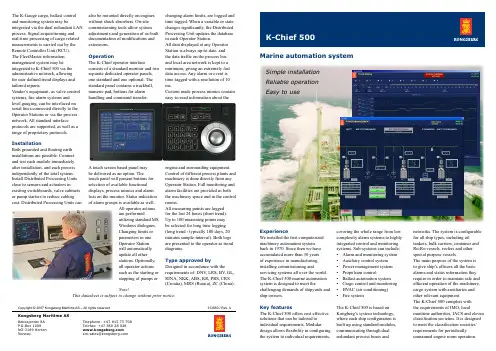
312850aa_kchief500_datasheet_email_version
- 格式:pdf
- 大小:816.49 KB
- 文档页数:2

DDR3L SDRAMMT41K1G4 – 128 Meg x 4 x 8 banksMT41K512M8 – 64 Meg x 8 x 8 banks MT41K256M16 – 32 Meg x 16 x 8 banksDescriptionDDR3L SDRAM (1.35V) is a low voltage version of the DDR3 (1.5V) SDRAM. Refer to DDR3 (1.5V) SDRAM (Die Rev :E) data sheet specifications when running in 1.5V compatible mode.Features•V DD = V DDQ = 1.35V (1.283–1.45V)•Backward compatible to V DD = V DDQ = 1.5V ±0.075V –Supports DDR3L devices to be backward com-patible in 1.5V applications•Differential bidirectional data strobe•8n-bit prefetch architecture•Differential clock inputs (CK, CK#)•8 internal banks•Nominal and dynamic on-die termination (ODT) for data, strobe, and mask signals •Programmable CAS (READ) latency (CL)•Programmable posted CAS additive latency (AL)•Programmable CAS (WRITE) latency (CWL)•Fixed burst length (BL) of 8 and burst chop (BC) of 4 (via the mode register set [MRS])•Selectable BC4 or BL8 on-the-fly (OTF)•Self refresh mode•T C of 105°C–64ms, 8192-cycle refresh up to 85°C–32ms, 8192-cycle refresh at >85°C to 95°C–16ms, 8192-cycle refresh at >95°C to 105°C •Self refresh temperature (SRT)•Automatic self refresh (ASR)•Write leveling•Multipurpose register•Output driver calibrationOptions Marking •Configuration– 1 Gig x 41G4–512 Meg x 8512M8–256 Meg x 16256M16•FBGA package (Pb-free) – x4, x8–78-ball (9mm x 10.5mm) Rev. E RH–78-ball (7.5mm x 10.6mm) Rev. N RG–78-ball (8mm x 10.5mm) Rev. P DA •FBGA package (Pb-free) – x16–96-ball (9mm x 14mm) Rev. E HA–96-ball (7.5mm x 13.5mm) Rev. N LY–96-ball (8mm x 14mm) Rev. P TW •Timing – cycle time–938ps @ CL = 14 (DDR3-2133)-093– 1.07ns @ CL = 13 (DDR3-1866)-107– 1.25ns @ CL = 11 (DDR3-1600)-125•Operating temperature–Commercial (0°C T C +95°C)None–Industrial (–40°C T C +95°C)IT–Automotive (–40°C T C +105°C)AT •Revision:E/:N/:PTable 1: Key Timing ParametersNotes: 1.Backward compatible to 1600, CL = 11 (-125).2.Backward compatible to 1866, CL = 13 (-107).Table 2: AddressingFigure 1: DDR3L Part Numbers([DPSOH 3DUW 1XPEHU 07 . 0 '$ 3Note:1.Not all options listed can be combined to define an offered product. Use the part catalog search on for available offerings.4Gb: x4, x8, x16 DDR3L SDRAMDescription质量等级领域:宇航级IC、特军级IC、超军级IC、普军级IC、禁运IC、工业级IC,军级二三极管,功率管等;应用领域:航空航天、船舶、汽车电子、军用计算机、铁路、医疗电子、通信网络、电力工业以及大型工业设备祝您:工作顺利,生活愉快!以深圳市美光存储技术有限公司提供的参数为例,以下为MT41K512M8DA-107_P的详细参数,仅供参考DDR3L 1.35V Slew Rate Definitions for Differential Input SignalsInput slew rate for differential signals (CK, CK# and DQS, DQS#) are defined and meas-ured, as shown in Table 31 and Figure 22. The nominal slew rate for a rising signal isdefined as the slew rate between V IL,diff,max and V IH,diff,min. The nominal slew rate for afalling signal is defined as the slew rate between V IH,diff,min and V IL,diff,max.Table 31: DDR3L 1.35V Differential Input Slew Rate DefinitionOutput Driver ImpedanceThe output driver impedance is selected by MR1[5,1] during initialization. The selected value is able to maintain the tight tolerances specified if proper ZQ calibration is per-formed. Output specifications refer to the default output driver unless specifically sta-ted otherwise. A functional representation of the output buffer is shown below. The out-put driver impedance R ON is defined by the value of the external reference resistor RZQ as follows:•R ON,x = RZQ /y (with RZQ = 240ȍ ±1%; x = 34ȍ or 40ȍ with y = 7 or 6, respectively)The individual pull-up and pull-down resistors R ON(PU) and R ON(PD) are defined as fol-lows:•R ON(PU) = (V DDQ - V OUT )/|I OUT |, when R ON(PD) is turned off •R ON(PD) = (V OUT )/|I OUT |, when R ON(PU) is turned offFigure 28: Output DriverOutput driverChip in drive mode V DDQV SSQV OUT DQ4Gb: x4, x8, x16 DDR3L SDRAMOutput Driver Impedance。
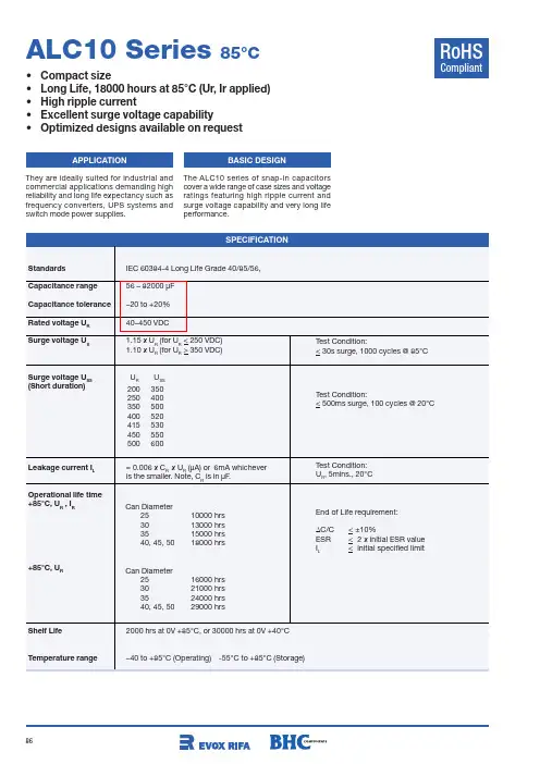

OX-2281-EAE-5000-20M000OCXONominal frequency (f0)20MHzFeaturesApplication•SC Cut Crystal •hermetically sealed •SMD•S3E compliant according GR1244•Wander generation (Standard /ZLAN Group)MTIE &TDEV compliant with:-G.8272(zG1&zG2)Performance SpecificationsAbsolute Maximum Ratings ParameterMinT ypical Max Units Supply voltage (Vs) 5.5VOperable temperature range-40+85◦C Storage temperature range -40+85◦CEnclosure4567321Top ViewH 0,37,62 0,117,8 0,10,223,4 0,17,62 0,117,8 0,1PadvorschlagrecommendationG3432,52,50,082,73,4-Pad Thickness 6030 mas long as the non-Pins/Pads area is higher.If the non-Pins/Pads area is lower, it adds to the coplanarity.all units in mmSolder profileNotes:Unless otherwise stated all values are valid after warm-up time and refer to typical conditions for supply voltage, frequency control voltage,load,temperature(25◦C).Subject to technical modification.USA:Europe:100Watts Street LandstrasseMt Holly Springs,P A1706574924NeckarbischofsheimGermanyTel:1.717.486.3411T el:+49(0)7268.801.0Fax:1.717.486.5920Fax:+49(0)7268.801.281Information contained in this publication regarding device applications and the like is provided only foryour convenience and may be superseded by updates.It is your reasonability to ensure that yourapplication meets with your specifications.MICROCHIP MAKES NO REPRESENT A TION ORWARRANTIES OF ANY KIND WHETHER EXPRESS OR IMPLIED,WRITTEN OR ORAL,ST ATUTORYOR OTHERWISE,RELA TED TO THE INFORMA TION INCLUDING,BUT NOT LIMITED TO ITSCONDITION,QUALITY,PERFORMANCE,MERCHANT ABILITY OR FITNESS FOR PURPOSE.Microchip disclaims all liability arising from this information and its e of Microchip devices in lifesupport and/or safety applications is entirely at the buyer’s risk,and the buyer agrees to defend,indemnify and hold harmless Microchip from any and all damages,claims,suits,or expenses resultingfrom such use.No licenses are conveyed,implicitly,or otherwise,under any Microchip intellectualproperty rights unless otherwise statedTrademarksThe Microchip and Vectron names and logos are registered trademarks of Microchip TechnologyIncorporated in the U.S.A.and other countries.List of appendicesAppendix_OX-228-EAE-5000-20M000_Jitter II Appendix_OX-228_MTIE_TDEV III Appendix_OX-2281-EAE-5000-20M000_I2C_V1.0VII Appendix handling&processing note XIIOX-2281-EAE-5000-20M0000M000The following MTIE TDEV plots were generated from data collected on production devices over the course of a year and represent typical performance. Frequency is measured every second and converted to phase using Microchip’s golden standard TimeMonitor soft ware. Filtering is applied to the data per standards requirements, and limits where applicable, are shown in red. Additional information on standards and oscillatorrecommendations can be found in ZLAN-830 and ZLAN-3467 (formerly ZLAN-442 and ZLAN-68).Const. Temp ±1°K; slope 0,1°C/min, range 21..23°C Const. Temp ±5°F; slope 0,1°C/min,range 19.22..24.78°C Trapezoid_Pattern_slope 0,5°C/min,range +2,5...42,5°C Triangle-Pattern_slope 0,2°C/min,range -40...85°CConst. Temp ±1°K; slope 0,1°C/min, range 21..23°C Const. Temp ±5°F; slope 0,1°C/min,range 19.22..24.78°C Trapezoid_Pattern_slope 0,5°C/min,range +2,5...42,5°C Triangle-Pattern_slope 0,2°C/min,range -40...85°CConst. Temp ±1°K; slope 0,1°C/min, range 21..23°C Const. Temp ±5°F; slope 0,1°C/min,range 19.22..24.78°C Trapezoid_Pattern_slope 0,5°C/min,range +2,5...42,5°C Triangle-Pattern_slope 0,2°C/min,range -40...85°CConst. Temp ±1°K; slope 0,1°C/min, range 21..23°C Const. Temp ±5°F; slope 0,1°C/min,range 19.22..24.78°C Trapezoid_Pattern_slope 0,5°C/min,range +2,5...42,5°C Triangle-Pattern_slope 0,2°C/min,range -40...85°C2The I2C interface option is available since manufacturing DC 2301The I2C interface shall be compliant with the I2C-Bus specification for standard speed operation. I2C Bus Voltage V I2C= 3.0VI²C-Device interface (SDA, SCL) Characteristics22Following the Start condition from the master, the device code (7 bits) and the R/W bit is placed onto the bus by the master transmitter. This indicates to the addressed slave receiver that 2 bytes with a word address (little endian format) will follow once it has generated an Acknowledge bit during the ninth clock cycle. Therefore, the next 2 bytes transmitted by the master is the word address and will be written into the Address Pointer of the slave device. After receiving another Acknowledge signal from the slave device, the master device will transmit the data word to be written into the addressed memory location. The slave device acknowledges again and the master generates a Stop condition. This initiates the internal write cycle and, during this time, the slave device will not generate Acknowledge signals.AP2.2 Page write operationThe write control byte, word address and the first data byte are transmitted to the slave device in the same way as in a byte write. However, instead of generating a Stop condition, the master transmits up to 16 data bytes to the slave device, which are temporarily stored in the on chip page buffer and will be written into memory once the master has transmitted a Stop condition. Upon receipt of each word, the Address Pointer bits are internally incremented by ‘1’. As with the byte write operation, once the Stop condition is received an internal write cycle will beginAP2.3 Acknowledge pollingSince the device will not acknowledge during a write cycle, this can be used to determine when the cycle is complete (this feature can be used to maximize bus throughput). Once the Stop condition for a Write command has been issued from the master, the device initiates the internally-timed write cycle and ACK polling can then be initiated immediately. This involves the master sending a Start condition followed by the control byte for a Write command (R/W = 0). If the device is still busy with the write cycle, no ACK will be returned. If the cycle is complete, the device will return the ACK and the master can then proceed with the next Read or Write command. See the figure below for a flow diagram of this operation.AP2.4 Current address readThe slave device contains an address counter that maintains the address of the last word accessed, internally incremented by ‘1’. Therefore, if the previous access (either a read or write operation) was to address n, the next current address read operation would access data from address n + 1. Upon receipt of the slave address with R/W bit set to ‘1’, the slave device issues an acknowledge and transmits the 8-bit data word. The master willnot acknowledge the transfer, but does generate a Stop condition and the slave device discontinues transmission.AP2.5 Random readRandom read operations allow the master to access any memory location in a random manner. To perform this type of read operation, the word address must first be set. This is accomplished by sending the 2 byte word address to the slave device as part of a write operation. Once the word address is sent, the master generates a Start condition following the acknowledge. This terminates the write operation, but not before the internal Address Pointer is set. The master then issues the control byte again, but with the R/W bit set to a ‘1’. The slave device will then issue an acknowledge and transmit the 8-bit data word. The master will not acknowledge the transfer, but does generate a Stop condition and the slave device will discontinue transmission.AP2.6 Sequential readSequential reads are initiated in the same way as a random read, except that once the slave device transmits the first data byte, the master issues an acknowledge as opposed to a Stop condition in a random read. This directs the slave device to transmit the next sequentially addressed 8-bit word.ApplicationUnless otherwise noted, the products listed in the catalogue are designed for use with ordinary electrical devices, such as stationary and portable communication, control, measurement equipment etc.. They are designed and manufactured to meet a high degree of reliability (lifetime more than 15 years) under normal …commercial“ application conditions. Products dedicated for automotive and H-Rel applications are specifically identified for these applications. If you intend to use these …commercial“ products for airborne, space or critical transport applications, nuclear power control, medical devices with a direct impact on human life, or other applications which require an exceptionally high degree of reliability or safety, please contact the manufacturer.Electrostatic SensitivityCrystal oscillators are electrostatic sensitive devices. Proper handling according to the established ESD handling rules as in IEC 61340-5-1 and EN 100015-1 is mandatory to avoid degradations of the oscillator performance due to damages of the internal circuitry by electrostatics. If not otherwise stated, our oscillators meet the requirements of the Human Body Model (HBM) according to JESD22-A114F.HandlingExcessive mechanical shocks during handling as well as manual and automatic assembly have to be avoided. If the oscillator was unintentionally dropped or otherwise subject to strong shocks, please verify that the electrical function is still within specification.Improper handling may also detoriate the coplanarity of bended leads of SMD components. SolderingOscillators can be processed using conventional soldering processes such as wave soldering, convection, infrared, and vapour phase reflow soldering under normal conditions. Solderability is guaranteed for one year storage under normal climatic conditions (+5°C to +35°C @ 40% to 75% relative humidity), however typically sufficient solderability –depending on the process – is maintained also for longer time periods. In cases of doubt, components older than one year should undergo a sample solderability test.The recommended reflow solder profile for SMT componets is according IPC/JEDEC J-STD-020 (latest revision)SMD oscillators must be on the top side of the PCB during the reflow process.After reflow soldering the frequency of the products may have shifted several ppm, which relaxes after several hours or days, depending on the products. For details please contact the manufacturer.CleaningCleaning is only allowed for hermetically sealed oscillators. Devices with non hermetical enclosures (e.g. with trimmer holes) shall not be cleaned by soaking or in vapour, because residues from the cleaning process may penetrate into the interior, and degrade the performance.Our products are laser marked. The marking of our oscillators is resistant to usual solvents, such as given in IEC 60068-2-45 Test XA. For applicable test conditions see IEC 60679-1.Ultrasonic cleaning is usually not harmful to oscillators at ultrasonic frequencies of 20kHz at the sound intensities conventional in industry. Sensitive devices may suffer mechanical damage if subjected to 40kHz ultrasound at high sound pressure. In cases of doubt, please conduct tests under practical conditions with the oscillators mounted on the PC board.Hermetical SealIf the device is specified as hermetically sealed, it meets the requirements of IEC 60679-1, i.e. for enclosures with a volume smaller than 4000mm³ the leak rate is below 5*10-8 bar cm3/s, for larger enclosures it is below 1*10-6 bar c bar cm3/s, tested according to IEC 60068-2-17 Test Qk.Glass feed-throughs may be damaged as a result of mechanical overload, such as bending the connection leads or cutting them with an unappropriated tool. In order to avoid microcracking, the wire must be held fixed in position by a pressure pad between glass feed-through and the bending point during the bending process. Check: there should be no damaged edges on the glass feed-through after the bending.Tape & ReelThe packing in tape and reel is according to IEC 60286-3.Details see tape & reel data sheets.QualificationVectron products are undergoing regular qualification/reliability tests as per product family definition. Results are available upon request. Customer specific qualification tests are subject to agreement.If not otherwise stated, the product qualifications are performed according to IEC 60679-5 or other valid industry standards.ScreeningOur oscillators are 100% tested, and all key manufacturing processes are controlled by Statistical Process Control (SPC). Additional screening is therefore usually not required.On request, we can perform screening tests according to MIL-PRF-55310, class B for discrete or hybrid constructions of commercial (COTS) products. For special requirements see the High Reliability Clock section.Demounting/Desoldering of Ocsillator device for analysis:The removal or desoldering of oscillators from customer application after SMT process may cause damage to the device if not handeld appropriately. It may lead to parametric change such as frequency shift (like OCXO: up to +/- 200 ppb) . It is utmost important to minimize the direct heat exposure to the device in order to avoid such effects. Use of hot air gun for desoldering should be avoided.A mechanical stress could also destroy the part, if exposed to excessive mechanical shock after removal process. Appropriate shock protection & ESD designated packaging must be used to avoid any external mechanical shock for FA return process.In general, the products* withstand the tests listed in the following Table 1, which are based on valid industry standards.*Additional note: Test conditions could vary for different product families and individual product specifications depending on the customer as well as product requirements.Recommended Environmental Test ConditionsTable 1。
