TLP3062(S)_datasheet_en_20101001
- 格式:pdf
- 大小:161.50 KB
- 文档页数:6
Unit: mm
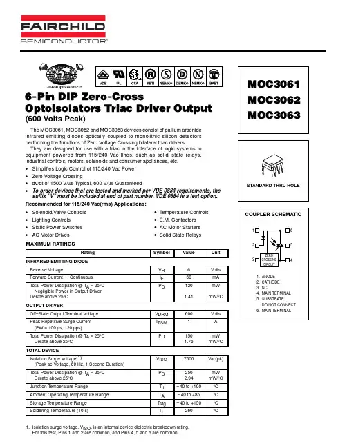
The TOSHIBA TLP3061 (S), TLP3062 (S), TLP3063 (S) consist of a zero voltage crossing turn-on photo-triac optically coupled to a gallium arsenide infrared emitting diode in a six lead plastic DIP package.
JEDEC
―
JEITA
―
TOSHIBA
11-7A9
weight: 0.39g (typ.)
Pin Configuration (top view)
1
6
2
3
ZC
4
1: Anode 2: Cathode 3: N.C. 4:Terminal 1 6:Terminal 2
ZC:Zero-cross Circuit
: BS EN60065, File No.8385
BS EN60950, File No.8386
• Option (D4) type
VDE approved: DIN EN60747-5-2
Approved No. 40009302
Maximum operating insulation voltage: 890VPK
Isolation voltage
Symbol
Test Condition
IFT
VT = 6 V
VIH
IF = rated IFT
IIH
IF = rated IFT VT = rated VDRM
CS
VS = 0, f = 1 MHz
RS
VS = 500 V (R.H.≤ 60%)
AC, 1 minute
1.2
300 −4.0 115 −55 to 150 −40 to 100 260 330
−4.4
A
mW mW / °C
°C °C °C °C mW
mW / °C
5000
Vrms
Note: Using continuously under heavy loads (e.g. the application of high temperature/current/voltage and the significant change in temperature, etc.) may cause this product to decrease in the reliability significantly even if the operating conditions (i.e. operating temperature/current/voltage, etc.) are within the absolute maximum ratings. Please design the appropriate reliability upon reviewing the Toshiba Semiconductor Reliability Handbook (“Handling Precautions”/“Derating Concept and Methods”) and individual reliability data (i.e. reliability test report and estimated failure rate, etc).
LED
Power dissipation
Power dissipation derating (Ta ≥ 25°C)
Reverse voltage
Junction temperature
Off−state output terminal voltage
On−state RMS current
Ta = 25°C Ta = 70°C
Power dissipation deratire
Storage temperature range
Operating temperature range
Lead soldering temperature (10 s)
Total package power dissipation
IF – Ta
60
50
40
30
20
10
0
-20
0
20
40
60
80 100 120
Ambient temperature Ta (℃)
IFP – DR
200
Vin = 60 Vrms, IT = 15mA (Fig.1)
―
Typ. 1.15 ― 10 10 1.7 0.6 500
0.2
Max. Unit
1.3
V
10
μA
―
pF
1000 nA
3.0
V
―
mA
― V / μs
― V / μs
Detector
Coupled Electrical Characteristics (Ta = 25°C)
TLP3061(S),TLP3062(S),TLP3063(S)
TOSHIBA PHOTOCOUPLER GaAs IRED & PHOTO-TRIAC
TLP3061(S),TLP3062(S),TLP3063(S)
OFFICE MACHINE HOUSEHOLD USE EQUIPMENT TRIAC DRIVER SOLID STATE RELAY
Highest permissible over voltage: 8000VPK
(Note):When a EN60747-5-2 approved type is needed, please designate the "Option (D4)"
• Construction mechanical rating
Symbol
Test Condition
Min.
VF IR CT IDRM VTM IH
dv / dt
dv / dt (c)
IF = 10 mA
1.0
VR = 5 V
―
V = 0, f = 1 MHz
―
VDRM = 600 V
―
ITM = 100 mA
―
―
―
Vin = 240 Vrms, Ta = 85°C (Fig.1)
BVS
AC, 1 second, in oil
DC, 1 minute, in oil
Min. Typ. Max. Unit
―
―
15
―
5
10
mA
―
―
5
―
―
50
V
―
100 300 μA
―
0.8
―
5×10¹⁰ 1014
―
5000
―
―
― 10000 ―
― 10000 ―
pF Ω Vrms Vdc
Fig. 1 dv / dt test circuit
Total package power dissipation derating (Ta ≥ 25°C)
Isolation voltage (AC, 1 min., R.H.≤ 60%)
(Note 1)
Symbol IF
ΔIF / °C IFP PD
ΔPD / °C VR Tj
VDRM
IT(RMS)
(Note 1) Device considered a two terminal device: Pins 1, 2 and 3 shorted together and pins 4 and 6 shorted together.
Recommended Operating Conditions
Characteristic
1
2010-10-01
TLP3061(S),TLP3062(S),TLP3063(S)
Absolute Maximum Ratings (Ta = 25°C)
Characteristic
Forward current
Forward current derating (Ta ≥ 53°C)
Peak forward current (100 μs pulse, 100 pps)
• Peak Off-State Voltage : 600 V (min)
• Trigger LED Current
: 15 mA (max) (TLP3061(S)) 10 mA (max) (TLP3062(S)) 5 mA (max) (TLP3063(S))
• On-State Current
※ In the case of TLP3062
2
2010-10-01
TLP3061(S),TLP3062(S),TLP3063(S)
Individual Electrical Characteristics (Ta = 25°C)
LED
Characteristic
Forward voltage Reverse current Capacitance Peak off−state current Peak on−state voltage Holding current Critical rate of rise of off−state voltage Critical rate of rise of commutating voltage
7.62 mm pich Standard Type
Creepage Distance Clearance Insulation Thickness