BK1080 Datasheet v3.2
- 格式:pdf
- 大小:1.40 MB
- 文档页数:45

ZXCT1080High voltage high-side current monitorDescriptionOrdering informationThe ZXCT1080 is a high side current sense monitor with a gain of 10 and a voltage output. Using this device eliminates the need to disrupt the ground plane when sensing a load current.The wide input voltage range of 60V down to as low as 3V make it suitable for a range of applications; including systems operating from industrial 24-28V rails and -48V rails.The separate supply pin (V CC ) allows the device to continue functioning under short circuit conditions, giving an end stop voltage at the output.The ZXCT1080 has an extended ambient operating temperature range of -40°C to 125°C enabling it to be used in a wide range of applications including automotive.Features•3V to 60V continuous high side voltage •Accurate high-side current sensing •-40 to 125°C temperature range •Output voltage scaling x10• 4.5V to 12V V CC range •Low quiescent current:•70µA supply pin •50µA I SENSE+•SOT23-5 package Applications•Industrial applications current measurement •Battery management •Over current monitor •Power management•Automotive current measurementPin connectionsTypical application circuitDevicePackage Part mark Reel size (inches)Tape width (mm)Quantity perreelZXCT1080E5TASOT23-51080783000https://Absolute maximum ratingsContinuous voltage on S- and S+-0.6 and 65V Voltage on all other pins-0.6V and +14VDifferential sense voltage, V SENSE 800mV Operating temperature -40 to 125°C Storage temperature-55 to 150°C Maximum junction temperature 125°CPackage power dissipation300mW * at T A = 25°COperation above the absolute maximum rating may cause device failure. Operation at the absolute maximum ratings, for extended periods, may reduce device reliability.V SENSE is defined as the differential voltage between S+ and S- pins.*Assumes ⍜JA = 420°C/WRecommended operating conditionsPin function tableParameterMin.Max.Units V IN Common-mode sense+ input range 360V V CCSupply voltage range4.512V V SENSE Differential sense input voltage range 00.15V V OUT Output voltage range 0 1.5V T AAmbient temperature range-40125°CPin Name Description1V CC This is the analogue supply and provides power to internal circuitry 2GND Ground pin3OUT Output voltage pin. NMOS source follower with 20µA bias to ground 4S+This is the positive input of the current monitor and has an input range from 60V down to 3V. The current through this pin varies with differential sense voltage5S-This is the negative input of the current monitor and has an input range from 60V down to 3Vhttps://Electrical characteristicsTest conditions T A = 25°C, V IN = 12V, V CC = 5 V, V SENSE (a) = 100mV unless otherwise stated.NOTES:(a)V SENSE = "V SENSE+" - "V SENSE-"(b)The ZXCT1080 operates from a positive power rail and the internal voltage-current converter current flow is unidirectional; these result in the output offset voltage for V SENSE = 0V always being positive.(c)For V SENSE > 10mV, the internal voltage-current converter is fully linear. This enables a true offset to be defined and used. V O(10) is expressed as the variance about an output voltage of 100mV>(d)Temperature dependent measurements are extracted from characterization and simulation results.(e)All Min and Max specifications over full temperature range are guaranteed by design and characterisationSymbol ParameterConditions T A Min (e).Typ.Max (e).Units I CC V CC supply current V CC = 12V, V SENSE (a) = 0V 25°C 4080120µAfull range 145I S+S+ input current V SENSE (a) = 0V25°C 152742µA full range 60I S-S- input current25°C 154080nA V O(0)Zero V SENSE (a) error (b)25°C 035mV V O(10)Output offset voltage (c)V SENSE (a) = 10mV 25°C -25+25mV full range -55+55Gain⌬V OUT /⌬V SENSE (a)V SENSE (a) = 10mV to150mV 25°C 9.91010.1V/V full range9.810.2V OUT TC (d)V OUT variation withtemperature 30ppm/°C Acc Total output error -33%I OH Output source current⌬V OUT = -30mV 1mA I OL Output sink current⌬V OUT = +30mV20µA PSRR V CC supply rejection ratioV CC = 4.5V to 12V 5460dB CMRR Common-mode sense rejection ratio V IN = 60V to 3V 6880dB BW-3dB small signal bandwidthV SENSE (a) (AC) = 10mV PP500kHz https://Typical characteristicsTest conditions unless otherwise stated: T A = 25°C, V CC = 5V, V SENSE+ =12V, V SENSE = 100mVTypical characteristicsTest conditions unless otherwise stated: T A = 25°C, V CC = 5V, V SENSE+ =12V, V SENSE = 100mVTypical characteristicsTest conditions unless otherwise stated: T A = 25°C, V CC = 5V, V SENSE+ =12V, V SENSE = 100mVhttps://Application informationThe ZXCT1080 has been designed to allow it to operate with 5V supply rails while sensing common mode signals up to 60V. This makes it well suited to a wide range of industrial and power supply monitoring applications that require the interface to 5V systems while sensing much higher voltages.To allow this its V CC pin can be used independently of S+.Figure 1 shows the basic configuration of the ZXCT1080.Figure 1Typical configuration of ZXCT1080Load current from the input is drawn through R SENSE developing a voltage V SENSE across the inputs of the ZXCT1080.The internal amplifier forces V SENSE across internal resistance R GT causing a current to flow through MOSFET M1. This current is then converted to a voltage by R G . A ratio of 10:1 between R G and R GT creates the fixed gain of 10. The output is then buffered by the unity gain buffer.The gain equation of the ZXCT1080 is:The maximum recommended differential input voltage, V SENSE , is 150mV; it will howeverwithstand voltages up to 800m ⍀. This can be increased further by the inclusion of a resistor, R LIM ,between S- pin and the load; typical value is of the order of 10k .V OUT I L R SENSE R GRGT---------1×I L R SENSE ×10×==https://Figure 2Protection/error sources for ZXCT1080Capacitor C D provides high frequency transient decoupling when used with R LIM ; typical values are of the order 10pFFor best performance R SENSE should be connected as close to the S+ (and SE NSE ) pins;minimizing any series resistance with R SENSE .When choosing appropriate values for R SENSE a compromise must be reached between in-line signal loss (including potential power dissipation effects) and small signal accuracy.Higher values for R SENSE gives better accuracy at low load currents by reducing the inaccuracies due to internal offsets. For best operation the ZXCT1080 has been designed to operate with V SENSE of the order of 50mV to 150mV.Current monitors' basic configuration is that of a unipolar voltage to current to voltage converter powered from a single supply rail. The internal amplifier at the heart of the current monitor may well have a bipolar offset voltage but the output cannot go negative; this results in current monitors saturating at very low sense voltages.As a result of this phenomenon the ZXCT1080 has been specified to operate in a linear manner over a V SENSE range of 10mV to 150mV range, however it will still be monotonic down to VSENSE of 0V.It is for this very reason that Zetex has specified an input offset voltage (V O(10)) at 10mV. The output voltage for any V SENSE voltage from 10mV to 150mV can be calculated as follows:Alternatively the load current can be expressed as:V OUT V SENSE ()xG V O 10()+=I L V OUT V O 10()–()GxR SENSE------------------------------------------=https://Package details - SOT23-5Note: Controlling dimensions are in millimeters. Approximate dimensions are provided in inchesDIM MillimetersInchesMin.Max.Min.Max.A - 1.00-0.0393A10.010.100.00030.0039A20.840.900.03300.0354b 0.300.450.01180.0177c 0.120.200.00470.0078D 2.90 BSC 0.114 BSCE 2.80 BSC 0.110 BSC E1 1.60 BSC 0.062 BSC e 0.95 BSC 0.0374 BSC e1 1.90 BSC0.0748 BSCL 0.300.500.01180.0196L20.25 BSC 0.010 BSC a°4°12°4°12°https://ZXCT1080DefinitionsProduct changeZetex Semiconductors reserves the right to alter, without notice, specifications, design, price or conditions of supply of any product or service. Customers are solely responsible for obtaining the latest relevant information before placing orders.Applications disclaimerThe circuits in this design/application note are offered as design ideas. It is the responsibility of the user to ensure that the circuit is fit for the user’s application and meets with the user’s requirements. No representation or warranty is given and no liability whatsoever is assumed by Zetex with respect to the accuracy or use of such information, or infringement of patents or other intellectual property rights arising from such use or otherwise. Zetex does not assume any legal responsibility or will not be held legally liable (whether in contract,tort (including negligence), breach of statutory duty, restriction or otherwise) for any damages, loss of profit, business, contract,opportunity or consequential loss in the use of these circuit applications, under any circumstances.Life supportZetex products are specifically not authorized for use as critical components in life support devices or systems without the express written approval of the Chief Executive Officer of Zetex Semiconductors plc. As used herein:A. Life support devices or systems are devices or systems which:1.are intended to implant into the bodyor 2.support or sustain life and whose failure to perform when properly used in accordance with instructions for use provided in thelabelling can be reasonably expected to result in significant injury to the user.B. A critical component is any component in a life support device or system whose failure to perform can be reasonably expected tocause the failure of the life support device or to affect its safety or effectiveness.ReproductionThe product specifications contained in this publication are issued to provide outline information only which (unless agreed by the company in writing) may not be used, applied or reproduced for any purpose or form part of any order or contract or be regarded as a representation relating to the products or services concerned.Terms and ConditionsAll products are sold subjects to Zetex’ terms and conditions of sale, and this disclaimer (save in the event of a conflict between the two when the terms of the contract shall prevail) according to region, supplied at the time of order acknowledgement.For the latest information on technology, delivery terms and conditions and prices, please contact your nearest Zetex sales office.Quality of productZetex is an ISO 9001 and TS16949 certified semiconductor manufacturer.To ensure quality of service and products we strongly advise the purchase of parts directly from Zetex Semiconductors or one of our regionally authorized distributors. For a complete listing of authorized distributors please visit: /salesnetworkZetex Semiconductors does not warrant or accept any liability whatsoever in respect of any parts purchased through unauthorized sales channels.ESD (Electrostatic discharge)Semiconductor devices are susceptible to damage by ESD. Suitable precautions should be taken when handling and transporting devices.The possible damage to devices depends on the circumstances of the handling and transporting, and the nature of the device. The extent of damage can vary from immediate functional or parametric malfunction to degradation of function or performance in use over time.Devices suspected of being affected should be replaced.Green complianceZetex Semiconductors is committed to environmental excellence in all aspects of its operations which includes meeting or exceeding regulatory requirements with respect to the use of hazardous substances. Numerous successful programs have been implemented to reduce the use of hazardous substances and/or emissions.All Zetex components are compliant with the RoHS directive, and through this it is supporting its customers in their compliance with WEEE and ELV directives.Product status key:“Preview”Future device intended for production at some point. Samples may be available“Active”Product status recommended for new designs“Last time buy (LTB)”Device will be discontinued and last time buy period and delivery is in effect“Not recommended for new designs”Device is still in production to support existing designs and production“Obsolete”Production has been discontinuedDatasheet status key:“Draft version”This term denotes a very early datasheet version and contains highly provisional information, which may change in any manner without notice.“Provisional version”This term denotes a pre-release datasheet. It provides a clear indication of anticipated performance.However, changes to the test conditions and specifications may occur, at any time and without notice.“Issue”This term denotes an issued datasheet containing finalized specifications. However, changes tospecifications may occur, at any time and without notice.https://。


WELDWRAPProtects Vulnerable Welding Hoses From Catastrophic Failure.Techflex WeldWrap (WW) is braided from fiberglass yarns with high temperature coating and velcro closure. Commonly used for protecting welding hoses against flame and abrasion, when dragging weld slag across the floor. This product willwithstand continuous exposure to temperatures of 400°F/204.4°C, and intermittent introduction to temperatures of 750°F/399°C.The heavy duty hook and loop closure ensures a tight seal and allows WeldWrap to be installed easily over existing assemblies. WeldWrap also provides a high level of abrasion and penetration protection to increase the useful life of any hoses exposed to rough or abrasive surfaces.Fiberglass Material WWN Grade .04”Wall Thickness ScissorsCut Cleanly 800.323.5140 • 973.300.9242 • fax: 973.300.940929 Brookfield Dr • Sparta, NJ 07871Braided Sleeving ProductsColors Available:Black (BK)...bundles and protects hoses and cables on welding robots and static welding stations.Nominal SizePart #Velcro WidthBulk SpoolShop SpoolRetailBagAvailable ColorsLbs/100’1”WWN1.00BK 0.84”150’50’25’10’Black 8.41 1/2”WWN1.50BK 0.84”150’50’25’10’Black 11.02”WWN2.00BK 1.55”150’50’25’10’Black 13.82 3/8”WWN2.38BK 1.55”150’50’25’10’Black 14.82 3/4”WWN2.75BK 1.55”150’50’25’10’Black 16.43”WWN3.00BK 1.55”150’50’25’10’Black 18.43 1/4”WWN3.25BK 1.55”150’50’25’10’Black 19.23 1/2”WWN3.50BK 1.55”150’50’25’10’Black 20.44”WWN4.00BK1.55”150’50’25’10’Black21.7Put-UpsE asy To Install - Cuts WithScissorsR esists Damage from UV,Gasoline & Engine Chemicals W eld Splatter, Hot Slag, & Welding Spark ProtectionS tays Flexible In Low Temps芯天下--/WELDWRAPIntermitten Exposure750°F (399°C) Maximum ContinuousMil-I-23053400°F (204.4°C)Minimum Continuous-40°F (-40°C)Abrasion Resistance HighAbrasion Test Machine Taber 5150 Abrasion Test Wheel Calibrase H-18 Abrasion Test Load 500gRoom Temperature 77°FHumidity70%Material Destroyed -Two Small Holes Worn Through1,060 Test Cycles Pre-Test Weight7,857.40 mgPost-Test Weight 6,602.20 mgTest End Loss Of Mass Point Of Destruction 1,255.20 mg 1=No Effect 4=More Affected2=Little Effect 5=Severely Affected3=AffectedAromatic Solvents ________________1Aliphatic Solvents ________________1Chlorinated Solvents ______________1Weak Bases ____________________1Salts __________________________1Strong Bases____________________1Salt Water 0-S-1926_______________1Hydraulic Fluid MIL-H-5606 _________1Lube Oil MIL-L-7808 _______________1De-Icing Fluid MIL-A-8243 __________1Strong Acids ____________________2Strong Oxidants _________________2Esters/Keytones _________________1UV Light _______________________1Petroleum ______________________1Fungus ASTM G-21________________1Rating ________Non FlammableMonofilament Diameter__________NAASTM D-204Flammability Rating___________VW-1FMVSS-302 ApprovedRecommended Cutting__Scissor/ShearsColors_________________________1Wall Thickness_________________.04© 2009 Techflex, Inc. - Any unauthorized reproduction, in whole or part, in any medium whatsoever, without the express written permission of Techflex, Inc. is strictly forbidden.T echflex product names and logos are registered trademarks of T echflex, Inc., unless otherwise attributed. The contents and illustrations contained herein are believed to be reliable. T echflex makes no warranties as to their accuracy or completeness and disclaims any liability in connection with their use. T echflex’s only obligations are those in standard terms of sale for these products and T echflex will not be liable for any consequential or other damages arising due to misuse of these products or typographical errors or omissions.Users should make their own evaluation to determine the suitability of these products for their unique and specific applications.09-09芯天下--/。

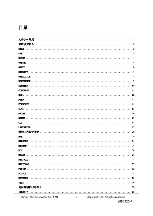
目录文件字体规则 (1)系统设定指令 (2)SIZE (2)GAP (3)BLINE (4)OFFSET (5)SPEED (6)DENSITY (7)DIRECTION (8)REFERENCE (9)COUNTRY (10)CODEPAGE (11)CLS (12)FEED (13)FORMFEED (14)HOME (15)PRINT (16)SOUND (17)CUT (18)LIMITFEED (19)卷标内容设计指令 (20)BAR (20)BARCODE (21)BITMAP (25)BOX (26)ERASE (27)DMATRIX (28)MAXICODE (29)PDF417 (32)PUTPCX (34)REVERSE (35)TEXT (36)询问打印机状态指令 (38)<ESC>!? (38)~!A (40)~!T (41)~!C (42)~!I (43)~!F (44)~!@ (45)信息传递协议 (46)<ESC>! (46)<ESC>& (46)~# (47)WINDOWS DRIVER驱动程序指令 (48)!B (48)!J (49)!N (50)档案管理指令 (51)DOWNLOAD (51)REDRAW (59)EOP (60)FILES (61)KILL (62)MOVE (63)UPDATBIOS (64)BASIC 指令及函式 (65)ABS( ) (65)ASC( ) (66)CHR$( ) (67)END (68)EOF( ) (69)OPEN (71)READ (73)SEEK (75)LOF( ) (77)FREAD$( ) (77)FOR...NEXT.. (79)IF...THEN...ELSE (81)GOSUB...RETURN. (83)GOTO (85)INPUT (88)REM (90)OUT (91)GETKEY( ) (92)INT( ) (93)LEFT$( ) (94)LEN( ) (95)MID$( ) (96)RIGHT$( ) (97)STR$( ) (98)VAL( ) (99)BEEP (100)打印机外围功能设定指令 (101)SET COUNTER (101)SET CUTTER (103)SET KEY1 (105)SET KEY2 (105)SET LED1, LED2, LED3 (107)SET PEEL (108)SET DEBUG (109)SET GAP (110)SET RIBBON (111)SET COM1 (112)@LABEL (114)PEEL (115)LED1, LED2, LED3 (116)KEY1, KEY2 (117)YEAR (118)MONTH (119)DATE (120)WEEK (121)HOUR (122)MINUTE (123)SECOND (125)文件字体规则本文件使用以下字体规则文件规则描述[表示内容] 在`中括号内表示该参数为选项<ESC> <ESC>代表ASCII 27 字符,当打印机收到以该控制字符为启始之指令将立即响应(即使打印机在错误状态时也将实时回应)~ (ASCII 126), 该字符启始的指令用于询问打印机的状态注: 200 DPI: 1 mm = 8 dots 粗斜体Arial,字型,用于表300 DPI: 1 mm = 12 dots 示批注DOWNLOAD “TEST.BAS”当所列出的内容为程序SET COUNTER @1 1 时以Curier 字型表示@1=”0001”TEXT 10,10,”3”,0,1,1,@1PRINT 3,2EOP系统设定指令SIZE说明该指令用于设定卷标纸的宽度及长度指令语法(1) 英制系统(英寸)SIZE m, n(2) 公制系统(公厘)SIZE m mm, n mm参数说明m 标签纸的宽度 (不含背纸)n 标签纸的长度 (不含背纸)Note: 200 DPI: 1 mm = 8 dots*300 DPI: 1 mm = 12 dots范例(1) 英制系统 (英寸)SIZE 3.5, 3.00(2) 公制系统 (公厘)SIZE 100 mm, 100 mmGAP说明该指令定义两张卷标纸间的垂直间距距离指令语法(1) 英制系统 (英寸)GAP m, n(2) 公制系统 (公厘)GAP m mm, n mm参数说明m 两标签纸中间的垂直距离0 ≤ m ≤ 1 (英寸), 0 ≤ m ≤ 25.4 (公厘)n 垂直间距的偏移[-]n ≤标签纸张长度 (英寸或公厘)Note: 200 DPI : 1 mm = 8 dots300 DPI : 1 mm = 12 dots范例一般垂直间距设定(1) 英制系统 (英寸)GAP 0.12,0(2) 公制系统 (公厘)GAP 3 mm,0特殊垂直间距设定(1) 英制系统 (英寸)GAP 0.30,-0.10(2) 公制系统 (公厘)GAP 7.62 mm, -2.54 mmBLINE说明该指令用于设定黑标的高度及偏移位置指令语法(1) 英制系统 (英寸)BLINE m, n(2) 公制系统 (公厘)BLINE m mm, n mm参数说明m 黑标的高度,以英寸或公厘表示0.1 ≤m ≤1 (英寸), 2.54 ≤m ≤ 25.4 (公厘)n 黑标偏移量 0 ≤n ≤标签纸张高度范例(1) 英制系统 (英寸)BLINE 0.20,0.50(2) 公制系统 (公厘)BLINE 5.08 mm,12.7 mmOFFSET说明该指令用于控制在剥离模式时(pee-off mode)每张卷标停止的位置,该指令仅适用于剥离模式。
Connect the BatteryBattery ReplacementThe battery typically lasts for two to five years, a shorter period if subjected to frequent outages or elevated temperatures. Battery replacement part for Back-UPS NS 1080 is APCRBC123. Please recycle spent battery cartridges.Install PowerChute ™ Personal Edition Software1.Connect the supplied USB software interface cable to the data port, and the other end to a computer with access to the internet.2.Go to /tools/download.3.Select PowerChute Personal Edition. Then select the appropriate operating system and follow the instructions to download the software.InventorySafety and General InformationInspect the package contents upon receipt. Notify the carrier and dealer if there is any damage.Read the Safety Guide supplied with this unit before installing the UPS.• This UPS is intended for indoor use only.• Do not operate this UPS in direct sunlight, in contact with fluids, or where there is excessive dust or humidity.• Be sure the air vents on the UPS are not blocked. Allow adequate space for proper ventilation.• The battery typically lasts for two to three years. Environmental factors impact battery life. Elevated ambient temperatures, poor quality AC power, and frequent short duration discharges will shorten battery life.• Connect the UPS power cable directly to a wall outlet. Do not use surge protectors or extension cords.Connect the EquipmentBattery Backup and Surge Protected outletslimited time from the Back-UPS.Connect equipment such as printers, fax machines,scanners, or other peripherals that do not need batteryBack-UPS is switched OFF.Master and Controlled outletsTo conserve electricity, when the device connected toMaster Outlet goes into Sleep or Standby mode, or turnsOff, the Controlled device(s) will shut down as well,saving electricity.Connect a master device, such as a desktop computer oraudio/visual receiver to the Master outlet. Connectto the Controlled outlets.Data port To use PowerChute Personal Edition, connect the supplied USB cable.Ground screw Connect the ground lead of additional surge suppression devices such as network and dataline surge protectors.Building Wiring Fault indicator If this indicator is illuminated, there is a problem with the wiring in the building. Contact an electrician immediately and do not use the Back-UPS.Surge Protected outlets, controlled by the Masteroutlet These outlets are protected from electrical surges, and will disconnect from AC power during a power outage, or if the Master device goes into Sleep or Standby mode.Surge Protected outlets These outlets provide full-time protection from surges, even if the Back-UPS is off. Connectequipment such as printers and scanners that do not require battery backup protection.Battery Backup outlets with Surge Protection During a power outage or other AC problems, the Battery Backup outlets receive power for a limited time from the Back-UPS. Connect critical equipment such as desktop computer, computer monitor, modem or other data sensitive devices into these outlets.Master outlet Connect the master device to this outlet, in most scenarios, this will be the main computer.In & Out Tel/Network surge-protected ports Use a telephone or network cable to connect a cable modem to the I N port, and connect a computer to the O UT port.Co-axial ports with surgeprotectionConnect a cable modem or other equipment with coaxial jacks.Back-UPS NS 10802OperationPower-Saving FunctionTo conserve electricity, configure the Back-UPS to recognize a Master device, such as a desktop computer or an A/ Array V receiver, and Controlled peripheral devices, such as a printer, speakers, or a scanner. When the Master device goesinto Sleep or Standby mode, or is switched OFF, the Controlled device(s) will be switched off as well, savingelectricity.Enable the Power-Saving function. Press and hold M UTE and D ISPLAY simultaneously for two seconds. The Back-UPSwill beep to indicate that the feature is enabled. The leaf icon on the display will illuminate.Disable the Power-Saving function. Press and hold M UTE and D ISPLAY simultaneously for two seconds. The Back-UPSwill beep to indicate that the feature is disabled. The leaf icon on the display will darken.Setting the threshold. The amount of power used by a device in Sleep or Standby mode varies between devices. It may be necessary to adjust the threshold at which the Master outlet signals the Controlled outlets to shut down.1.Ensure a master device is connected to the Master outlet. Put that device into Sleep or Standby mode, or turn it OFF.2.Press D ISPLAY and M UTE simultaneously and hold for six seconds, until the leaf icon flashes three times and the Back-UPS beeps three times.3.The Back-UPS will now recognize the threshold level of the Master device and save it as the new threshold setting. Power-Saving displayThe display interface can be configured to be continuously illuminated, or to save energy, it can be configured to darken after a period of inactivity.1.Full Time Mode: Press and hold DISPLAY for two seconds. The display will illuminate and the Back-UPS will beep toconfirm the Full-Time mode.2.Power-Saving Mode: Press and hold DISPLAY for two seconds. The display will darken and the Back-UPS will beep toconfirm the Power-Saving mode. While in Power-Saving Mode, the display will illuminate if a button is pressed, it thendarkens after 60 seconds of no activity.Unit sensitivityAdjust the sensitivity of the Back-UPS to control when it will switch to battery power; the higher the sensitivity, the more often the Back-UPS will switch to battery power.1.Ensure the Back-UPS is connected to AC power, but is OFF.2.Press and hold the P OW ER button for six seconds. The L OAD C APACITY bar will flash on and off, indicating that the Back-UPS is in programming mode.3.Press P OW ER again to rotate through the menu options. Stop at selected sensitivity. The Back-UPS will beep to confirm theselection.Back-UPS NS 10803Front panel buttons and display interfaceUse the three buttons on the front panel of the Back-UPS and the display interface to configure the Back-UPS.Front panel Array Mute buttonPower On/OffbuttonDisplay buttonDisplay interface4Back-UPS NS 1080Warnings and System FaultsAudible warningsFour Beeps Every 30 Seconds Back-UPS is running on battery. You should consider saving any work in progress. Continuous Beeping Low battery condition and battery run-time is very low. Promptly save any work in progress,exit all open applications, and shut down the operating system.Continuous tone Battery Backup outputs are overloaded.Chirps for 1 Minute every 5 hours Battery fails the automatic diagnostic test and should be replaced.Warning iconsSystem faultsThe Back-UPS will display these fault messages. For faults F01 and F02, contact Schneider Electric (SEIT)Technical Support.Back-UPS NS 10805Function Button Quick-ReferenceFunction Button Timing(seconds)UPSStatus DescriptionPowerPower On0.2Off Press P OW ER to start receiving input AC power. If A/C input power isnot available, the Back-UPS will run on battery power.Power Off2On The Back-UPS is not receiving input AC power, but is providingsurge protection.DisplayStatus Inquiry0.2On Verify the status or condition of the Back-UPS. The LCD willilluminate for 60 seconds.Full-Time/Power-Saving mode 2On The LCD will illuminate and the Back-UPS will beep to confirm theFull-Time mode. The LCD will darken and the Back-UPS will beepto confirm the Power-Saving mode. While in Power-Saving Mode,the LCD will illuminate if a button is pressed, then darkens after 60seconds of no activity.MuteEvent Specific0.2On Disable any audible alarms caused by an event.General Status Enable/Disable 2On Enable or disable the audible alarms. The Mute icon will illuminateand the Back-UPS will beep one time. The Mute function will notactivate unless the Back-UPS is operating on battery power.Sensitivity6Off The Load Capacity icon will blink, indicating that the Back-UPS is inprogramming mode. Use the P OW ER button to scroll through Low,Medium, and High, stop at selected sensitivity. TheBack-UPS will beep to confirm selection. See Configuration fordetails.Master/Controlled outlet Enable/Disable 2On The leaf icon will darken indicating that the Master Outlet feature isdisabled or illuminate to indicate the Master Outlet feature isenabled. The Back-UPS will beep once.Master/Enable Threshold Calibration 6On While calibrating the threshold setting, the device connected to theMaster Outlet should be turned off or placed in Standby or Sleepmode. Upon completion, Power-Saving icon will flash 3 and beep 3timesSelf-Test (manual)6On The Back-UPS will perform a test of the internal battery. Note: Thiswill happen automatically when the Back-UPS is turned ON. Event Reset0.2On When the Event screen is visible, press and hold D ISPLAY, thenpress POW ER, to clear the AC failure event counter.Fault Reset2Fault After a fault has been identified, press P OW ER to remove the visualindication and return to standby statusBack-UPS NS 10806TroubleshootingProblem Possible Cause Corrective ActionBack-UPS will not switch on.The Back-UPS is not connected to ACpower.Ensure that the Back-UPS is securely connected to anAC outlet.The circuit breaker has been tripped.Disconnect non-essential equipment from theBack-UPS. Reset the circuit breaker. Re-connectequipment one item at a time. If the circuit breaker istripped again, disconnect the device that caused the trip. The internal battery is not connected.Connect the battery.The AC input voltage is out of range.Adjust the transfer voltage and sensitivity range.The Back-UPS does not provide power during a AC power outage.Ensure that essential equipment is notplugged into a S URGE O NLY outlet.Disconnect equipment from the S URGE O NLY outlet andre-connect to a Battery Backup outlet.The Back-UPS is operating on battery power, while connected to AC power.The plug has partially pulled out of the walloutlet, the wall outlet is no longer receivingAC power, or the circuit breaker has beentripped.Ensure that the plug is fully inserted into the wall outlet.Ensure that the wall outlet is receiving AC power bychecking it with another device.The Back-UPS is performing an automaticself test.No action is necessary.The AC input voltage is out of range, thefrequency is out of range, or the waveform isdistorted.Adjust the transfer voltage and sensitivity range.The Back-UPS does not provide the expected amount of backup time.Battery Backup outlets may be fully orimproperly loaded.Disconnect non-essential equipment from the BatteryBackup outlets and connect the equipment to S URGEO NLY outlets.The battery was recently discharged due to apower outage and has not fully recharged.Charge the battery cartridge for 16 hours.The battery has reached the end of its usefullife.Replace the battery.The R EPLACE B ATTERY indicator is illuminated.The battery has reached the end of its usefullife.Replace the battery.The O VERLOAD indicator is illuminated.The equipment connected to the Back-UPSis drawing more power than the Back-UPScan provide.Disconnect non-essential equipment from the BatteryBackup outlets and connect the equipment to S URGEO NLY outlets.The S YSTEM F AULT indicator is illuminated, all the front panel indicators are flashing.There is an internal fault.Determine which internal fault message is displayed bymatching the number displayed on the LCD with thecorresponding Fault Message (see System Faults) andcontact SEIT Technical Support.Power is not supplied to some outlets.Power to the Controlled outlets hasintentionally been turned off.Confirm that the correct peripherals are connected toControlled outlets. If this feature is not desired, disablethe Power-Saving Master and Controlled outlets.The Controlled outlets are not supplying power, even though the Master device is not in sleep mode.The Master Outlet threshold may beincorrectly set.Adjust the threshold when the Master outlet signals theControlled outlets to shut down.Back-UPS NS 10807© 2013 APC by Schneider Electric. APC, the APC logo, PowerChute, and Back-UPS are owned by Schneider Electric Industries S.A.S., or their affiliated companies. All other trademarks are property of their respective owners.EN 990-4837A07/2013SpecificationsWarrantyThe standard warranty is three (3) years from the date of purchase. Schneider Electric IT (SEIT) standard procedure is to replace the original unit with a factory reconditioned unit. Customers who must have the original unit back due to the assignment of asset tags and set depreciation schedules must declare such a need at first contact with an SEIT Technical Support representative. SEIT will ship the replacement unit once the defective unit has been received by the repair department, or cross ship upon the receipt of a valid credit card number. The customer pays for shipping the unit to SEIT. SEIT pays ground freight transportation costs to ship the replacement unit to the customer.APC by Schneider Electric IT Customer Support WorldwideFor country specific customer support, go to the APC by Schneider Electric Web site, .Select models are ENERGY STAR ® qualified.For more information go to/site/recycle/index.cfm/energy-efficiency/energy-star/.This UPS is certified to comply with California Battery Charger System regulations.For more information go to/site/recycle/index.cfm/energy-efficiency/cec-battery-charger/.EMC ComplianceThis device complies with part 68 and part 15 of the FCC rules. Operation is subject to the following two conditions: (1) This device may not cause harmful interference, and(2) This device must accept any interference received, including interference that may cause undesired operation.Locate the label on the bottom of this device that contains, among other information, the FCC registration number and ringer equivalence number (REN) for this device. If requested, this information must be provided to the telephone company.If you experience trouble with this equipment, you disconnect it from the network until the problem has been corrected or until you are sure that the equipment is not malfunctioning. The ringer equivalence number (REN) is used to determine how many devices can be connected to your telephone line. In most areas, the sum of the RENs of all devices on any one line should not exceed five (5.0). If too many devices are attached, they may not ring properly.VA1080 VA Maximum Load 650 W Nominal Input Voltage 120 V Online Input Voltage Range88 - 139 VAutomatic Voltage Regulation (98-107) +11.2%Frequency Range 60 Hz ± 1 HzOn-battery Waveshape Step-approximated sine-wave Typical Recharge Time 16 hoursTransfer Time8 ms (typical), 10 ms (maximum)Operating Temperature 0 to 40 C (32 to 104 F) Storage Temperature -5 to 45 C (23 to 113 F) Unit Dimensions 25 × 10 × 38.2 cm (9.84 × 3.93 × 15.0 in) Unit Weight 10.7 kg (23.6 lbs)InterfaceUSBOn-Battery RuntimeGo to: /ServiceIf the unit requires service, do not return it to the dealer. Follow these steps:1.Review the Troubleshooting section of the manual to eliminate common problems.2.If the problem persists, contact Schneider Electric IT (SEIT) Customer Support through the APC by Schneider Electric Web site, .a.Note the model number and serial number and the date of purchase. The model and serial numbers are located on the rear panel of the unit and are available through the LCD display on select models.b.Call SEIT Customer Support and a technician will attempt to solve the problem over the phone. If this is not possible, the technician will issue a Returned Material Authorization Number (RMA#).c.If the unit is under warranty, the repairs are free.d.Service procedures and returns may vary internationally. Refer to the APC by Schneider Electric Web site for country specific instructions.3.Pack the unit in the original packaging whenever possible to avoid damage in transit. Never use foam beads for packaging. Damage sustained in transit is not covered under warranty.4.Always DISCONNECT THE UPS BATTERIES before shipping. The United States Department of Transportation (DOT), and the International Air Transport Association (IATA) regulations require that UPS batteries bedisconnected before shipping. The internal batteries may remain in the UPS.5.Write the RMA# provided by Customer Support on the outside of the package.6.Return the unit by insured, pre-paid carrier to the address provided by Customer Support。
BK1080v3.2BK1080SpecificationsBeken Internal Data — Signed NDA Required for DistributionFM Receiver ICBeken CorporationSuite 3A, No.1278 Keyuan Road, Zhangjiang High Tech Park, Pudong New District,Shanghai 201203, ChinaThis document contains information that may be proprietary to, and/or secrets of, Beken Corporation. The contents of this document should not be disclosed outside the companies without specific written permission.Disclaimer: Descriptions of specific implementations are for illustrative purpose only, actual hardware implementation may differ.BK1080FM Receiver© 2011 Beken Corporation Proprietary and Confidential Page 2 of 45Content1 General Description .................................................................................................... 32 Features .......................................................................................................................3 3 Applications ................................................................................................................ 34 Chip Block Diagram ................................................................................................... 45 Pin Assignment ........................................................................................................... 5 6Functional Description .............................................................................................. 14 6.1 FM Receiver...................................................................................................... 14 6.2 Interface bus ...................................................................................................... 14 6.2.1 3-wire bus mode ............................................................................................ 14 6.2.2 I2C bus mode ................................................................................................ 14 6.3 Stereo audio processing .................................................................................... 15 6.4 Tuning System .................................................................................................. 16 6.5 Software Tuning System ................................................................................... 17 6.6 GPIO Output ..................................................................................................... 17 6.7 Reference clock ................................................................................................. 17 6.8 Initialization Sequence ...................................................................................... 17 7 Design Specification ................................................................................................. 19 7.1 Recommended Operating Conditions ............................................................... 19 7.2 Absolute Maximum Ratings ............................................................................. 19 7.3 Power Consumption Specification .................................................................... 19 7.4 Receiver Characteristics.................................................................................... 20 7.5 I2C Control Interface Characteristics ............................................................... 21 7.6 3-Wire Control Interface Characteristics .......................................................... 22 8 Register definition ..................................................................................................... 23 9 Typical Application Schematic ................................................................................. 28 10 Package information ................................................................................................. 35 11 Solder Reflow Profile ............................................................................................... 43 12 Order information ..................................................................................................... 44 13 Update History . (45)BK1080v3.21 General DescriptionThe BK1080 FM receiver employs a low-IF architecture, mixed signal image rejection and all digital demodulation technology. The station scan of BK1080 searches radio stations based on both the channel RSSI estimation and signal quality assessment, increases the number of receivable stations while avoids false stops. BK1080 enables FM radio reception with low power, small board space and minimum number of external components.All functions are controlled through a simple 3-wire serial interface or I2C serial interface. The device operates from a power supply of 2.5 – 5.5 volts.The BK1080 is available in 24-pin 4x4 mm QFN, 20-pin 3x3 mm QFN, 12-pin 2x2 mm QFN, TSSOP16, SOP16 and SOP8 packages.2 Features● Support 64~108 MHz band ● Automatic gain control● Automatic frequency control ● Seek tuning● Receive signal strength indicator ● Channel quality assessment ● Stereo decoder● Automatic stereo/mono switching ● Automatic noise suppression ● 50us/75us de-emphasis ● 2.5 ~ 5.5 V supply voltage● Wide range reference clock supported ● 32.768KHz crystal oscillator● I2C and 3-wires control interface ●4x4 mm 24-pin QFN package 3x3 mm 20-pin QFN package 2x2 mm 12-pin QFN package TSSOP 16-pin package SOP16-pin package SOP8-pin package3 Applications● Cellular handset ● MP3 player● PDAs and notebookBK1080FM Receiver© 2011 Beken Corporation Proprietary and Confidential Page 4 of 454 Chip Block DiagramBK1080v3.25 Pin AssignmentG P I O 3G P I O 2G P I O 1N CN C G N D© 2011 Beken Corporation Proprietary and Confidential Page 6 of 45BK1080v3.2G N DN CV A 1V A 2N CN C© 2011 Beken Corporation Proprietary and Confidential Page 8 of 45BK1080v3.2G P I O 2G P I O 1N CN CG N D© 2011 Beken Corporation Proprietary and Confidential Page 10 of 45G P I O 2G N DG N D© 2011 Beken Corporation Proprietary and Confidential Page 12 of 45© 2011 Beken Corporation Proprietary and Confidential Page 14 of 456 Functional Description6.1 FM ReceiverThe receiver employs a digital low-IF architecture that reduces external components, and integrates a low noise amplifier (LNA) supporting the worldwide FM broadcast band (65 to 108MHz), an automatic gain control (AGC) circuit controls the gain of the LNA to optimize sensitivity and rejection of strong interferers, an image-reject mixer down converts the RF signal to low-IF, The mixer output is amplified by a programmable gain control (PGA), and digitized by a high resolution analog-to-digital converters (ADCs). An audio DSP finishes the channel selection, FM demodulation, stereo MPX decoder and output audio signal. The MPX decoder can autonomous switch from stereo to mono to limit the output noise.6.2 Interface busThe BK1080 supports 3-wire and I 2C control interface, with up to 2.5 MHz clock speed. User could select either of them by setting the state of MODE pin. BK1080 will use I2C interface for MODE=0 or 3-wire interface for MODE =1. Note that BK1080XB, BK1080MB, BK1080NB, BK1080TB, BK1080SB, and BK1080VB package only support I2C interface mode.BK1080 always latches data at the rising edge of SCLK and outputs its data at the falling edge of SCLK. For MCU, data should be always written at the falling edge of SCLK, and read out at the rising edge of SCLK.6.2.1 3-wire bus modeWhen selecting 3-wire mode, user must set MODE = 1.3-wire bus mode uses SCLK, SDIO and SEN pins. A transaction begins when user drives SEN low. Next, user drives an 8-bit command serially on SDIO, which is captured by BK1080 on rising edges of SCLK. The command consists of a 7-bit start register address, followed by a read/write bit (read = 1, write = 0).6.2.2 I2C bus modeWhen selecting I2C mode, user must set MODE = 0.I2C bus mode only uses SCLK and SDIO pins. A transaction begins with the start condition, which occurs when SDIO falls while SCLK is high. Next, user drivers an 8-bit device ID serially on SDIO, which is captured by BK1080 at the rising edge of SCLK. The device ID of BK1080 is 0x80.After driving the device ID, user drives an 8-bit control word on SDIO. The control word consists of a 7-bit start register address, followed by a read/write bit (read = 1, write = 0).For I2C host reading, the host must give an ACK to BK1080 after each byte access, and should give a NACK to BK1080 after last byte read out. For stable communication, the rising edge time of SCLK should be less than 200ns.SCLKSENSDIOFigure 8 3-wire Interface Diagrama signal. Separate left and right channels are obtained by adding and subtracting the (L+R) and (L-R) signals, respectively. Adaptive noise suppression is employed to gradually combine the stereo left and right audio channels to a mono (L+R) audio signal as the signal quality degrades to maintain optimumover the ST be de-the is is frequencies. All FM receivers incorporate a de-emphasis filter which attenuates high frequencies to restore a flat frequency response. Two time constants, 50 or 75 μs , are used in various regions. The de-emphasis time constant is programmable with the DE bit. High-fidelity stereo digital-to-analog© 2011 Beken Corporation Proprietary and ConfidentialPage 16 of 45converters (DACs) drive analog audio signals onto the LOUT and ROUT pins. The audio output may be muted with the DMUTE bit. Volume can be adjusted digitally with the VOLUME [3:0] bits. The soft mute feature is available to attenuate the audio outputs and minimize audible noise in very weak signal conditions. The soft mute attack and decay rate can be adjusted with the SMUTER [1:0] bits where 00 is the fastest setting. The soft mute attenuation level can be adjusted with the SMUTEA [1:0] bits where 00 is the most attenuated. The soft mute disable (DSMUTE) bit may be set high to disable this feature.6.4 Tuning SystemChannel spacing of 50, 100 or 200 kHz is selected with bits SPACE [1:0]. The channel is selected with bits CHAN [9:0]. The bottom of the band is set to 76 MHz or 87.5 MHz with the bits BAND [1:0]. The tuning operation begins by setting the TUNE bit. After tuning completes, the seek/tune complete (STC) bit will be set and the RSSI level is available by reading bits RSSI [7:0]. The TUNE bit must be set low after the STC bit is set high in order to complete the tune operation and clear the STC bit. Seek tuning searches up or down for a channel with an RSSI greater than or equal to the seek threshold set with the SEEKTH [7:0] bits. In addition, an optional SNR and/or impulse noise detector may be used to qualify valid stations. The SKSNR [3:0] bits set the SNR threshold required. The SKCNT [3:0] bits set the impulse noise threshold. Using the extra seek qualifiers can reduce false stops and, in combination with lowering the RSSI seek threshold, increase the number offound stations. The SNR and impulse noise detectors are disabled by default. Two seek modes are available. When the seek mode (SKMODE) bit is low and a seek operation is initiated, the device seeks through the band, wraps from one band edge to the other, and continues seeking. If the seek operation was unable to find a channel, the seek failure/band limit (SF/BL) bit will be set high and the device will return to the channel selected before the seek operation began. When the SKMODE bit is high and a seek operation is initiated, the device seeks through the band until the band limit is reached and the SF/BL bit will be set high. A seek operation is initiated by setting the SEEK and SEEKUP bits. After the seek operation completes, the STC bit will be set, and the RSSI level and tuned channel are available by reading bits RSSI [7:0] and bits READCHAN [9:0]. During a seek operation READCHAN [9:0] is also updated and may be read to determine seek progress. The STC bit will be set after the seek operation completes. The channel is valid if the seek operation completes and the SF/BL bit is set low. At other times, such as before a seek operation or after a seek completes and the SF/BL bit is set high, the channel is valid if the AFC Rail (AFCRL) bit is set low and the value of RSSI [7:0] is greater than or equal to SEEKTH [7:0]. Note that if the AFCRL bit is set, the audio output is muted as in the soft mute case discussed in stereo audio processing section. The SEEK bit must be set low after the STC bit is set high in order to complete the seek operation and clear the STC and SF/BL bits. The seek operation may be aborted by setting the SEEK bit low at any time. The device can be configured to generate an interrupt on GPIO2 when a tune or seekoperation completes. Setting the seek/tune complete (STCIEN) bit and GPIO2 [1:0] = 01 will configure GPIO2 for a 5 ms low interrupt when the STC bit is set by the device.6.5 Software Tuning System The BK1080 also supports the software seek by tuning and judging every channels from MCU. The operation begins by setting the TUNE bit after tuning completes, the seek/tune complete (STC) bit will be set and the RSSI, SNR , IMPC and FREQD level is available by reading bits RSSI [7:0], SNR[3:0], IMPC[3:0] and FREQD[11:0].When all this parameters meet the thresholds which can set by MCU, it is a right station.6.6 GPIO OutputThe BK1080 has three GPIO pins. The function of GPIO pins could be programmed with bits GPIO1 [1:0], GPIO2 [1:0], GPIO3 [1:0], GPIO2/3 pins can be used as interrupt request pins for the seek/tune ready functions and as a stereo/mono indicator respectively. General purpose output functionality is available regardless of the state of the VA and VD supplies, or the ENABLE and DISABLE bits.6.7 Reference clockThe BK1080 series accepts wide range, from 32.768 kHz to 38.4 MHz, reference clock input to the RCLK pin. For frequency less than 4 MHz, it must be multiplier of 32.768K. The BK1080 series requires the V pk-pk of reference clock is higher than 500mV. BK1080 (except BK1080NB) also support 32.768KHz crystal oscillator input.6.8 Initialization Sequence To initialize BK1080:1.Supply VIO.2.Supply VA and VD. Note that VAand VD could be supplied at thesame time of VIO supplied.3.Provide RCLK.4.Set the ENABLE bit high and theDISABLE bit low to power upBK1080.To power down BK1080:1.Set the ENABLE bit high and theDISABLE bit high to place BK1080in power down mode. Note that allregister states are maintained solong as VIO is supplied.2.(Optional) Remove RCLK.3.Remove VA and VD as needed.To power up BK1080 (after power down):1.Note that VIO is still supplied in thisscenario. If VIO is not supplied,refer to BK1080 initializationprocedure above.2.Supply VA and VD.3.Provide RCLK.4.Set the ENABLE bit high and theDISABLE bit low to power upBK1080.© 2011 Beken Corporation Proprietary and Confidential Page 18 of 457 Design Specification7.1 Recommended Operating Conditions Table 7 Recommended Operating Conditions© 2011 Beken Corporation Proprietary and Confidential Page 20 of 457.4 Receiver CharacteristicsTable 10 Receiver Characteristics7.5 I2C Control Interface Characteristics Table 11 I2C Control Interface Characteristics© 2011 Beken Corporation Proprietary and Confidential Page 22 of 457.6 3-Wire Control Interface CharacteristicsTable 12 3-Wire Control Interface CharacteristicsAddress InData Out?Cycle Bus TurnaroundFigure 13 3-Wire Control Interface Read Timing Diagram8 Register definition Table 13 Register definition© 2011 Beken Corporation Proprietary and Confidential Page 24 of 45© 2011 Beken Corporation Proprietary and Confidential Page 26 of 45© 2011 Beken Corporation Proprietary and Confidential Page 28 of 459 Typical Application SchematicFB1(Crystal connection). Place C8 and crystal close to RCLK pin. Place C8 close to crystal.7. All grounds connect directly to GND plane on PCB. 8. Keep the FMIP trace as short as possible.9. Keep the wire from FMIN to headphone as short as possible and must put it on thesurface of the PCB.7.Keep the FMIP trace as short as possible.8.Keep the wire from FMIN to headphone as short as possible and must put it on thesurface of the PCB.9.Application with differential input improved system sensitivity 3dB.6.Place C3 and C4 close to chip pins.7.All grounds connect directly to GND plane on PCB.8.Keep the wire from FMIN to headphone as short as possible and must put it on thesurface of the PCB.© 2011 Beken Corporation Proprietary and Confidential Page 30 of 458.Keep the FMIN trace as short as possible.9.Keep the wire from FMIP to headphone as short as possible and must put it on thesurface of the PCB.© 2011 Beken Corporation Proprietary and Confidential Page 32 of 457.All grounds connect directly to GND plane on PCB.8.Keep the wire from FMIN to headphone as short as possible and must put it on thesurface of the PCB.© 2011 Beken Corporation Proprietary and Confidential Page 34 of 4510 Package informationWe have chosen QFN 4x4 24pin, QFN 3x3 20pin, QFN 2x2 12pin, TSSOP 16pin, SOP 16pin and SOP8 pin packages. Detail information of the package follows:© 2011 Beken Corporation Proprietary and Confidential Page 36 of 45Figure 23 QFN 2x2 12 Pin Package diagramFigure 24 TSSOP 16 Pin Package diagram© 2011 Beken Corporation Proprietary and Confidential Page 38 of 45© 2011 Beken Corporation Proprietary and Confidential Page 40 of 45Figure 26 SOP 8 Pin Package diagram© 2011 Beken Corporation Proprietary and Confidential Page 42 of 45Soldering Layer ContentStorage Caution1. Calculated shelf life in vacuum sealed bag 12 months at<40℃ and 90% relativehumidity(RH).2. Peak package body temperature 260℃.3. After vacuum sealed bag is opened ,devices that will be subjected to reflow solder orother high temperature process musta) Mounted within 168 hours of factory conditions<40℃/60%. b) Stored at 10% RH.11 Solder Reflow ProfilePBB&PBDE content in accordance with directive 2002/95/EC(RoHS).ESD SensitivityIntegrated circuits are ESD sensitive and can be damaged by static electricity. Proper ESD Techniques should be used when handling these devices.© 2011 Beken Corporation Proprietary and Confidential Page 44 of 4512 Order informationTable 17 BK1080 order information13 Update History。