PC7070K封装
- 格式:pdf
- 大小:112.78 KB
- 文档页数:1

DW07D 二合一锂电池保护IC一、 概述DW07D 产品是单节锂离子/锂聚合物高压可充电电池组保护的高集成度解决方案。
DW07D 包括了先进的功率MOSFET ,高精度的电压检测电路和延时电路。
DW07D 具有非常小的SOT23-6的封装,这使得该器件非常适合应用于空间限制得非常小的可充电电池组应用。
DW07D 具有过充,过放,过流,短路等所有的电池所需保护功能,并且工作时功耗非常低。
该芯片不仅仅是为手机而设计,也适用于一切需要锂离子或锂聚合物可充电电池长时间供电的各种信息产品的应用场合。
二、 特点¾ 内部集成等效50m Ω左右的先进的功率MOSFET ;¾ 3段过流保护:过放电流1、过放电流2(可选)、负载短路电流; ¾ 充电器检测功能; ¾ 允许0V 充电功能¾ 延时时间内部设定; ¾ 高精度电压检测;¾ 低静态耗电流:正常工作电流3.8uA ¾ 兼容ROHS 和无铅标准。
¾采用SOT23-6封装形式塑封。
三、 应用¾ 单芯锂离子电池组;¾ 锂聚合物电池组。
四、 订货信息型号封装过充检测电压 [V CU ](V ) 过充解除电压[V CL ](V )过放检测电压[V DL ](V )过放解除电压 [V DR ](V )过流 (A )打印标记DW07D SOT23-6 4.4 4.2 2.8 3.0 3A DW07D五、 引脚图及说明DW07D二合一锂电池保护IC六、 极限参数参数符号参数范围单位电源电压VDD VSS-0.3~VSS+12 V CSI输入管脚电压VCSI VDD+15~VDD+0.3 V 工作温度Topr -40~+85 ℃存储温度Tstg -40~+125 ℃七、 电气特性参数参数符号测试条件最小值典型值最大值单位工作电压工作电压VDD -- 1.5--10V 电流消耗工作电流IDD VDD= 3.9V --3.06.0 uA检测电压过充电检测电压A档VOCP --4.350 4.375V B档 4.375 4.400 4.425C档 4.425 4.450过充电释放电压VOCR -- 4.15 4.20 4.25 V 过放电检测电压VODP -- 2.72 2.80 2.88 V 过放电释放电压VODR -- 2.92 3.00 3.08 V 过电流1检测电压VOI1 -- 0.12 0.15 0.18 V 过电流2(短路电流)检测电压VOI2 VDD= 3.6V 0.80 1.00 1.20 V 过电流复位电阻Rshort VDD= 3.6V 50100150 KΩ过电器检测电压VCHA -- -0.8 -0.5 -0.2 V 向0V电池充电的功能充电器起始电压V0CH 允许向0V电池充电功能1.2 -- -- V迟延时间过充电检测迟延时间TOC VDD= 3.6V~4.4V -- 110 200 ms过放电检测迟延时间TOD VDD= 3.6V~2.0V -- 80 140 ms过电流1检测迟延时间TOI1 VDD= 3.6V 51320 ms过电流2(短路电流)检测迟延时间TOI2 VDD= 3.6V --550 usMOS参数单个MOS管漏极到源极的导通阻抗R DS(on) V GS = 2.5V, I D =0.5A-- 22.0 30.0 mΩR DS(on) V GS = 4.5V, I D = 1.0A-- 16.0 25.0过流I ODC VDD= 3.6V 2.0 3.0 4.0 A 漏-源击穿电压V(BR)DSS V GS = 0V, I D= 250μA19 20 -- V连续的漏极电流I D(DeviceRef.)T J= 25°C 5 ADW07D二合一锂电池保护IC 栅极阈值电压V GS(th)V DS=VGS, I D=250μA0.55 0.65 0.95 V漏-源极电流I DSS V DS=20V, V GS= 0V,T J= 25°C1 uA栅-源极电流I GSS V GS= ±10V 100 nA 八、功能描述DW07D监控电池的电压和电流,并通过断开充电器或负载,保护单节可充电锂电池不会因为过充电压,过放电压,过放电流以及短路等情况而损坏。
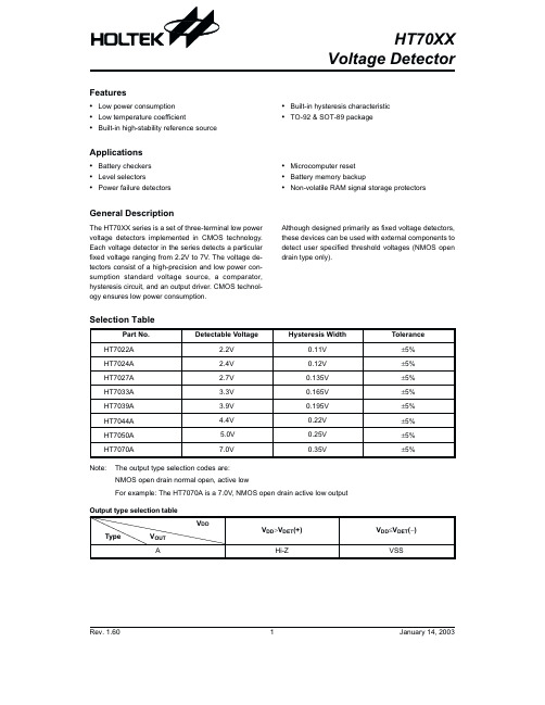
HT70XXVoltage DetectorSelection TablePart No.Detectable VoltageHysteresis WidthTolerance HT7022A 2.2V 0.11V ±5%HT7024A 2.4V 0.12V ±5%HT7027A 2.7V 0.135V ±5%HT7033A 3.3V 0.165V ±5%HT7039A 3.9V 0.195V ±5%HT7044A 4.4V 0.22V ±5%HT7050A 5.0V 0.25V ±5%HT7070A 7.0V0.35V±5%Note:The output type selection codes are:NMOS open drain normal open,active lowFor example:The HT7070A is a 7.0V,NMOS open drain active low outputOutput type selection tableV DDV DD >V DET (+)V DD £V DET (-)TypeV OUT AHi-ZVSSRev.1.601January 14,2003General DescriptionThe HT70XX series is a set of three-terminal low power voltage detectors implemented in CMOS technology.Each voltage detector in the series detects a particular fixed voltage ranging from 2.2V to 7V.The voltage de-tectors consist of a high-precision and low power con-sumption standard voltage source,a comparator,hysteresis circuit,and an output driver.CMOS technol-ogy ensures low power consumption.Although designed primarily as fixed voltage detectors,these devices can be used with external components to detect user specified threshold voltages (NMOS open drain type only).Features·Low power consumption ·Low temperature coefficient·Built-in high-stability reference source·Built-in hysteresis characteristic ·TO-92&SOT-89packageApplications·Battery checkers ·Level selectors ·Power failure detectors·Microcomputer reset ·Battery memory backup·Non-volatile RAM signal storage protectorsBlock DiagramN channel open drain output(normal open;active low)A typePin AssignmentRev.1.602January14,2003Pad AssignmentHT70XX (except HT7022A)Chip size:1317´1158(m m)2*The IC substrate should be connected to VDD in the PCB layout artwork.HT7022A onlyChip size:2032´1321(m m)2*The IC substrate should be connected to VDD in the PCB layout artwork.Absolute Maximum RatingsSupply Voltage,except HT7022A..................................................................................................V SS -0.3V to V SS +26V Supply Voltage,HT7022A only....................................................................................................................-0.3V to13V Output Voltage...........................V SS -0.3V to V DD +0.3V Output Current......................................................50mA Storage Temperature............................-50°C to 125°C Power Consumption..........................................200mWOperating Temperature 0°C to 70°CNote:These are stress ratings only.Stresses exceeding the range specified under ²Absolute Maximum Ratings ²maycause substantial damage to the device.Functional operation of this device at other conditions beyond those listed in the specification is not implied and prolonged exposure to extreme conditions may affect device reliabil-ity.Rev.1.603January 14,2003Pad CoordinatesHT70XX (except HT7022A)Unit:m m Pad No.X Y 1-483.30-379.502-234.60-399.503443.90-386.00HT7022A onlyUnit:m mPad No.X Y1-434.34394.972120.65461.013774.70412.75Electrical CharacteristicsHT7022A Ta=25°CHT7024A Ta=25°CHT7027A Ta=25°CRev.1.604January14,2003HT7039A Ta=25°CHT7044A Ta=25°CRev.1.605January14,2003HT7070A Ta=25°CRev.1.606January 14,2003Functional DescriptionThe HT70XX series is a set of voltage detectors equipped with a high stability voltage reference which is connected to the negative input of a comparator ¾de-noted as V REF in the following figure for NMOS output voltage detector.When the voltage drop to the positive input of the com-parator (i,e,V B )is higher than V REF ,VOUT goes high,M1turns off,and V B is expressed as V BH =V DD ´(R B +R C )/(R A +R B +R C ).If V DD is decreased so that V B falls to a value less than V REF ,the comparator output in-verts from high to low,V OUT goes low,V C is high,M1turns on,RC is bypassed,and V B becomes:V BL =V DD ´R B /(R A +R B ),which is less than V BH.By so doing,the comparator output will stay low to prevent the circuit from oscillating when V B »V REF.If V DD falls below the minimum operating voltage,the output becomes undefined.When VDD goes from low to V DD ´R B /(R A +R B )>V REF ,the comparator output and V OUT goes high.The detectable voltage is defined as:V DET (-)=R R R R R A B CB C +++´V REFThe release voltage is defined as:V DET (+)=R R R A BB+´V REFThe hysteresis width is:V HYS=V DET(+)-V DET(-)The figure demonstrates the NMOS output type withpositive output polarity(V OUT is normally open,activelow).The HT70XX series also supplies options for otheroutput types with active high outputs.Application cir-cuits shown are examples of positive output polarity(normally open,active low)unless otherwise specified.NMOS output voltage detector(HT70XXA) Application CircuitsMicrocomputer reset circuitNormally a reset circuit is required to protect the micro-computer system from malfunctions due to power line interruptions.The following examples show how differ-ent output configurations perform a reset function in var-ious systems.·NMOS open drain output application for separate power supply·NMOS open drain output application with R-C delayPower-on reset circuitWith several external components,the NMOS open drain type of the HT70XX series can be used to perform a power-on reset function as shown:Rev.1.607January14,20035V power line monitoring circuitGenerally,a minimum operating voltage of4.5V is guar-anteed in a5V power line system.The HT7044A is rec-ommended for use as5V power line monitoring circuit.·5V power line monitor with power-on reset·with5V voltage regulatorChange of detectable voltageIf the required voltage is not found in the standard prod-uct selection table,it is possible to change it by using ex-ternal resistance dividers or diodes.·Varying the detectable voltage with a resistance di-viderDetectable voltage=R RRA BB+´V DETHysteresis width=R RRA BB+´V HYS·Varying the detectable voltage with a diodeDetectable Voltage=V f1+V f2+V DETMalfunction analysisThe following circuit demonstrates the way a circuit ana-lyzes malfunctions by monitoring the variation or spikenoise of power supply voltage.Charge monitoring circuitThe following circuit shows a charged monitor for pro-tection against battery deterioration by overcharging.When the voltage of the battery is higher than the set de-tectable voltage,the transistor turns on to bypass thecharge current,protecting the battery from overcharg-ing.Rev.1.608January14,2003Level selectorThe following diagram illustrates a logic level selector.Rev.1.609January14,2003Package Information3-pin TO-92outline dimensionsSymbolDimensions in milMin.Nom.Max.A170¾200B170¾200C500¾¾D11¾20E90¾110F45¾55G45¾65H130¾160I8¾18a4°¾6°Rev.1.6010January14,20033-pin SOT-89outline dimensionsSymbolDimensions in milMin.Nom.Max.A173¾181B64¾72C90¾102D35¾47E155¾167F14¾19G17¾22H¾59¾I55¾63J14¾17Rev.1.6011January14,2003Product Tape and Reel SpecificationsTO-92reel dimensions(Unit:mm)Rev.1.6012January14,2003SOT-89reel dimensionsSOT-89Symbol Description Dimensions in mmA Reel Outer Diameter180±1.0B Reel Inner Diameter62±1.5C Spindle Hole Diameter12.75+0.15D Key Slit Width 1.9±0.15T1Space Between Flange12.4+0.2T2Reel Thickness17-0.4Rev.1.6013January14,2003TO-92Symbol Description Dimensions in mm I1Taped Lead Length(2.5)P Component Pitch12.7±1.0P0Perforation Pitch12.7±0.3P2Component to Perforation(Length Direction) 6.35±0.4F1Lead Spread 2.5+0.4-0.1F2Lead Spread 2.5+0.4-0.1D h Component Alignment0±0.1W Carrier Tape Width 18.0+1.0-0.5W0Hold-down Tape Width 6.0±0.5W1Perforation Position9.0±0.5W2Hold-down Tape Position(0.5)H0Lead Clinch Height16.0±0.5H1Component Height Less than24.7D0Perforation Diameter 4.0±0.2t Taped Lead Thickness0.7±0.2H Component Base Height19.0±0.5Note:Thickness less than0.38±0.05mm~0.5mmP0Accumulated pitch tolerance:±1mm/20pitches.()Bracketed figures are for consultation onlyRev.1.6014January14,2003SOT-89Symbol Description Dimensions in mmW Carrier Tape Width 12.0+0.3-0.1P Cavity Pitch8.0±0.1E Perforation Position 1.75±0.1F Cavity to Perforation(Width Direction) 5.5±0.05D Perforation Diameter 1.5+0.1D1Cavity Hole Diameter 1.5+0.1P0Perforation Pitch 4.0±0.1P1Cavity to Perforation(Length Direction) 2.0±0.10A0Cavity Length 4.8±0.1B0Cavity Width 4.5±0.1K0Cavity Depth 1.8±0.1t Carrier Tape Thickness0.30±0.013C Cover Tape Width9.3Rev.1.6015January14,2003Holtek Semiconductor Inc.(Headquarters)No.3,Creation Rd.II,Science-based Industrial Park,Hsinchu,TaiwanTel:886-3-563-1999Fax:886-3-563-1189Holtek Semiconductor Inc.(Sales Office)11F,No.576,Sec.7Chung Hsiao E.Rd.,Taipei,TaiwanTel:886-2-2782-9635Fax:886-2-2782-9636Fax:886-2-2782-7128(International sales hotline)Holtek Semiconductor(Shanghai)Inc.7th Floor,Building2,No.889,Yi Shan Rd.,Shanghai,ChinaTel:021-6485-5560Fax:021-6485-0313Holtek Semiconductor(Hong Kong)Ltd.RM.711,Tower2,Cheung Sha Wan Plaza,833Cheung Sha Wan Rd.,Kowloon,Hong KongTel:852-2-745-8288Fax:852-2-742-8657Holmate Semiconductor,Inc.48531Warm Springs Boulevard,Suite413,Fremont,CA94539Tel:510-252-9880Fax:510-252-9885CopyrightÓ2003by HOLTEK SEMICONDUCTOR INC.The information appearing in this Data Sheet is believed to be accurate at the time of publication.However,Holtek as-sumes no responsibility arising from the use of the specifications described.The applications mentioned herein are used solely for the purpose of illustration and Holtek makes no warranty or representation that such applications will be suitable without further modification,nor recommends the use of its products for application that may present a risk to human life due to malfunction or otherwise.Holtek reserves the right to alter its products without prior notification.For the most up-to-date information,please visit our web site at .Rev.1.6016January14,2003。

Low Cost MicroprocessorSupervisory Circuits Data Sheet ADM705/ADM706/ADM707/ADM708Rev. H Document FeedbackInformation furnished by Analog Devices is believed to be accurate and reliable. However, noresponsibility is assumed by Analog Devices for its use, nor for any infringements of patents or other rights of third parties that may result from its use. Specifications subject to change without notice. No license is granted by implication or otherwise under any patent or patent rights of Analog Devices. T rademarks and registered trademarks are the property of their respective owners. One Technology Way, P.O. Box 9106, N orwood, MA 02062-9106, U.S.A. Tel: 781.329.4700 ©2002–2016 Analog Devices, Inc. All rights reserved. Technical Support FEATURESGuaranteed RESET valid with V CC = 1 V190 μA quiescent currentPrecision supply voltage monitor4.65 V (ADM705/ADM707)4.40 V (ADM706/ADM708)200 ms reset pulse widthDebounced TTL/CMOS manual reset input (MR) Independent watchdog timer (ADM705/ADM706)1.60 sec timeout (ADM705/ADM706)Active high reset output (ADM707/ADM708)Voltage monitor for power fail or low battery warning Superior upgrade for MAX705 to MAX708 APPLICATIONSMicroprocessor systemsComputersControllersIntelligent instrumentsCritical microprocessor supply monitoringFUNCTIONAL BLOCK DIAGRAMSWATCHDOGINPUT (WDI)POWER-FAILINPUT (PFI)POWER-FAILOUTPUT (PFO)WATCHDOGOUTPUT (WDO)RESET*VOLTAGE REFERENCE = 4.65V (ADM705), 4.40V (ADM706)MRV CC88-1Figure 1. ADM705/ADM706POWER-FAIL*VOLTAGE REFERENCE = 4.65V (ADM707), 4.40V (ADM708)MRV CC88-2OUTPUT (PFO)Figure 2. ADM707/ADM708GENERAL DESCRIPTIONThe ADM705/ADM706/ADM707/ADM708 microprocessor supervisory circuits are suitable for monitoring 5 V power supplies/batteries and microprocessor activity.The ADM705/ADM706 provide power-supply monitoring circuitry that generate a reset output during power-up, power-down, and brownout conditions. The reset output remains operational with V CC as low as 1 V. Independent watchdog monitoring circuitry is also provided. This is activated if the watchdog input has not been toggled within 1.60 sec.In addition, there is a 1.25 V threshold detector to warn of power failures, to detect low battery conditions, or to monitor an additional power supply. An active low, debounced manual reset input (MR) is also included. The ADM705 and ADM706 are identical except for the reset threshold monitor levels, which are 4.65 V and 4.40 V, respectively. The ADM707 and ADM708 provide a similar functionality to the ADM705 and ADM706 and only differ in that a watchdog timer function is not available. Instead, an active high reset output (RESET) is available as well as the active low reset output (RESET). The ADM707 and ADM708 are identical except for the reset threshold monitor levels, which are 4.65 V and 4.40 V, respectively.All devices are available in narrow 8-lead PDIP and 8-lead SOIC packages.ADM705/ADM706/ADM707/ADM708Data SheetRev. H | Page 2 of 12TABLE OF CONTENTSFeatures .............................................................................................. 1 Applications ....................................................................................... 1 Functional Block Diagrams ............................................................. 1 General Description ......................................................................... 1 Revision History ............................................................................... 2 Specifications ..................................................................................... 3 Absolute Maximum Ratings ............................................................ 4 ESD Caution .................................................................................. 4 Pin Configurations and Function Descriptions ........................... 5 Typical Performance Characteristics ............................................. 6 Circuit Information .. (8)Power Fail RESET Output ............................................................8 Manual Reset ..................................................................................8 Watchdog Timer (ADM705/ADM706) .....................................8 Power Fail Comparator .................................................................8 Valid RESET Below 1 V V CC ........................................................9 Applications Information .............................................................. 10 Monitoring Additional Supply Levels ...................................... 10 Microprocessor with Bidirectional RESET ............................. 10 Outline Dimensions ....................................................................... 11 Ordering Guide .. (12)REVISION HISTORY1/16—Rev. G to Rev. HChanges to Table 3 ............................................................................ 5 Changes to Power Fail Comparator Section and Figure 15 ........ 8 Changes to Figure 16 ........................................................................ 9 Changes to Figure 18 and Figure 20 ............................................. 10 Updated Outline Dimensions ....................................................... 12 Changes to Ordering Guide . (12)3/08—Rev. F to Rev. GChanges to Applications .................................................................. 1 Changes to Table 2 ............................................................................ 4 Changes to Figure 9 .......................................................................... 6 Changes to Figure 10, Figure 11, and Figure 12 ........................... 7 Changes to Figure 14 ........................................................................ 8 Changes to Ordering Guide . (12)2/07—Rev. E to Rev. FUpdated Format .................................................................. U niversal Changes to Watchdog Timeout Period .......................................... 3 Replaced Pin Configurations and Function Descriptions Section .. 5 7/06—Rev. D to Rev. EAdded RM-8 (MSOP) Package ......................................... U niversal Changes to Table 2 ............................................................................. 4 Updated Outline Dimensions ....................................................... 12 Changes to Ordering Guide . (12)11/05—Rev. C to Rev. DUpdated Format .................................................................. U niversal Deleted Figure 2 ................................................................................. 4 Updated Outline Dimensions ....................................................... 11 Changes to Ordering Guide . (12)8/02—Rev. B to Rev. CRemoved RM-8 (µSOIC) Package .................................... U niversal Updated N-8 and R-8 Packages . (8)Data Sheet ADM705/ADM706/ADM707/ADM708 SPECIFICATIONSV CC = 4.75 V to 5.5 V, T A = T MIN to T MAX, unless otherwise noted.Rev. H | Page 3 of 12ADM705/ADM706/ADM707/ADM708Data SheetRev. H | Page 4 of 12ABSOLUTE MAXIMUM RATINGST A = 25°C, unless otherwise noted. Table 2.Parameter RatingV CC−0.3 V to +6 VAll Other Inputs −0.3 V to V CC + 0.3 V Input CurrentV CC 20 mA GND20 mA Digital Output Current20 mA Power Dissipation, N-8 PDIP 727 mW θJA Thermal Impedance 135°C/W Power Dissipation, R-8 SOIC 470 mW θJA Thermal Impedance110°C/W Power Dissipation, RM-8 MSOP 900 mW θJA Thermal Impedance206°C/W Operating Temperature RangeIndustrial (Version A)−40°C to +85°C Lead Temperature (Soldering, 10 sec) 300°C Vapor Phase (60 sec) 215°C Infrared (15 sec)220°CStorage Temperature Range −65°C to +150°C ESD Rating>4.5 kVStresses at or above those listed under Absolute Maximum Ratings may cause permanent damage to the product. This is a stress rating only; functional operation of the product at these or any other conditions above those indicated in the operational section of this specification is not implied. Operation beyond the maximum operating conditions for extended periods may affect product reliability.ESD CAUTIONData SheetADM705/ADM706/ADM707/ADM708Rev. H | Page 5 of 1200088-003Figure 3. ADM705/ADM706 PDIP/SOICPin Configuration00088-004NC = NO CONNECTFigure 4. ADM707/ADM708 PDIP/SOICPin Configuration00088-005RESET RESET MR V CC NC = NO CONNECTFigure 5. ADM708 MSOP Pin ConfigurationADM705/ADM706/ADM707/ADM708Data SheetRev. H | Page 6 of 12TYPICAL PERFORMANCE CHARACTERISTICS00088-012Figure 6. RESETOutput Voltage vs. Supply VoltageV CC RESET00088-013Figure 7. ADM707/ADM708 RESET Output Voltage vs. Supply Voltage1.2V0V5V1.3V PFIPFO00088-014500ns/DIVFigure 8. PFI Comparator Assertion Response Time1.3V 4.4V0V1.2VPFOPFI500ns/DIVFigure 9. PFI Comparator Deassertion Response Time5V0V00088-016100ns/DIVFigure 10. RESET , RESET Assertion5V0V5V0V00088-017100ns/DIVFigure 11. RESET , RESET DeassertionData SheetADM705/ADM706/ADM707/ADM708Rev. H | Page 7 of 124V0V2μs/DIV00088-018Figure 12. ADM705/ADM707 RESET Response TimeADM705/ADM706/ADM707/ADM708Data SheetRev. H | Page 8 of 12CIRCUIT INFORMATIONPOWER FAIL RESET OUTPUTRESET is an active low output that provides a reset signal to the microprocessor whenever the V CC input is below the reset threshold. An internal timer holds RESET low for 200 ms after the voltage on V CC rises above the threshold. This functions as a power-on reset signal for the microprocessor. It allows time for both the power supply and the microprocessor to stabilize after power-up. The RESET output is guaranteed to remain valid (low) with V CC as low as 1 V . This ensures that the microprocessor is held in a stable shutdown condition as the power supply voltage ramps up.In addition to RESET , an active high RESET output is also available on the ADM707/ADM708. This is the complement of RESET and is useful for processors requiring an active high reset signal.MANUAL RESETThe manual reset input (MR ) allows other reset sources, such as a manual reset switch, to generate a processor reset. The input is effectively debounced by the timeout period (200 ms typically). The MR input is TTL-/CMOS-compatible, so it can also be driven by any logic reset output.00088-007Figure 13. RESET , MR , and WDO TimingWATCHDOG TIMER (ADM705/ADM706)The watchdog timer circuit can monitor the activity of the micro-processor to check that it is not stalled in an indefinite loop. An output line on the processor toggles the watchdog input (WDI) line. If this line is not toggled within the timeout period (1.60 sec), then the watchdog output (WDO ) goes low. The WDO can be connected to a nonmaskable interrupt (NMI) on the processor; therefore, if the watchdog timer times out, an interrupt is gen-erated. The interrupt service routine then rectifies the problem. If a RESET signal is required when a timeout occurs, the WDO must connect to the manual reset input (MR ).The watchdog timer is cleared by either a high to low or a low to high transition on WDI. It is also cleared by RESET going low; therefore, the watchdog timeout period begins after RESET goes high.When V CC falls below the reset threshold, WDO is forced low, whether or not the watchdog timer has timed out. Normally, this generates an interrupt, but it is overridden by RESET going low. The watchdog monitor can be deactivated by floating the WDI. The WDO can then be used as a low line output because it goes low only when V CC falls below the reset threshold.00088-008Figure 14. Watchdog TimingPOWER FAIL COMPARATORThe power fail comparator is an independent comparator that can monitor the input power supply. The comparator inverting input is internally connected to a 1.25 V reference voltage. The noninverting input is available at the PFI input. This input can monitor the input power supply via a resistive divider network. When the voltage on the PFI input drops below 1.25 V , the comparator output (PFO ) goes low, indicating a power failure. For early warning of power failure, the comparator monitors the preregulator input by choosing an appropriate resistive divider network. The PFO output can interrupt the processor so a shutdown procedure is implemented before power is lost. As the voltage on the PFI pin is limited to V CC + 0.3 V , it is recommended to connect the PFI pin with a Schottky diode to the RESET pin as shown in Figure 15. This helps clamping the PFI pin voltage during device power up and operation.INPUT POWER00088-009Data SheetADM705/ADM706/ADM707/ADM708Rev. H | Page 9 of 12Adding Hysteresis to the Power Fail ComparatorFor increased noise immunity, hysteresis can be added to the power fail comparator. Because the comparator circuit isnoninverting, hysteresis can be added by connecting a resistor between the PFO output and the PFI input as shown in Figure 16.7V TO 15VINPUTLV INH 00088-010Figure 16. Adding Hysteresis to the Power Fail ComparatorWhen PFO is low, Resistor R3 sinks current from the summing junction at the PFI pin. When PFO is high, Resistor R3 sources current into the PFI summing junction. This results in differing trip levels for the comparator. Further noise immunity can be achieved by connecting a capacitor between PFI and GND. The equations calculate the hysteresis are as follows:⎥⎦⎤⎢⎣⎡⎪⎭⎫⎝⎛⨯++=R1R3R2R3R2V H 125.1 ⎪⎭⎫⎝⎛--+=R3V R2R1V CC L 25.125.125.1⎪⎭⎫⎝⎛+=R2R2R1V MID 25.1VALID RESET BELOW 1 V V CCThe ADM705/ADM706/ADM707/ADM708 are guaranteed to provide a valid reset level with V CC as low as 1 V (see the Typical Performance Characteristics section). As V CC drops below 1 V , the internal transistor does not have sufficient drive to hold the voltage RESET at 0 V . A pull-down resistor can connect externally, as shown in Figure 17, to hold the line low if required.00088-011Figure 17. RESET Valid Below 1 VADM705/ADM706/ADM707/ADM708Data SheetRev. H | Page 10 of 12APPLICATIONS INFORMATIONA typical application circuit is shown in Figure 18. The un-regulated dc input supply is monitored using PFI via the resistive divider network. Resistor R1 and Resistor R2 must be selected so when the supply voltage drops below the desired level (such as 8 V), the voltage on PFI drops below the 1.25 V threshold, thereby generating an interrupt to the microprocessor. Monitoring the preregulator input provides additional time to execute an orderly shutdown procedure before power is lost.7V00088-020Figure 18. Typical Application CircuitMicroprocessor activity is monitored using WDI. This is driven using an output line from the processor. The software routines toggle this line at least once every 1.60 seconds. If a problem occurs and this line is not toggled, WDO goes low and a nonmaskable interrupt is generated. This interrupt routine can clear the problem. If, in the event of inactivity on the WDI line, a system reset is required, WDO must connect to MR as shown in Figure 19.00088-021Figure 19. RESET From WDOMONITORING ADDITIONAL SUPPLY LEVELSIt is possible to use the power fail comparator to monitor a second supply as shown in Figure 20. The two sensing resistors, R1 and R2, are selected so the voltage on PFI drops below 1.25 V at the minimum acceptable input supply. PFO can connect to MR so a reset is generated when the supply drops out of tolerance. In this case, if either supply drops out of tolerance, a reset is generated.00088-022Figure 20. Monitoring 5 V and an Additional Supply, V XMICROPROCESSOR WITH BIDIRECTIONAL RESETTo prevent contention for microprocessors with a bidirectional reset line, a current limiting resistor must be inserted between the ADM705/ADM706/ADM707/ADM708 RESET output pin and the microprocessor RESET pin. This limits the current to a safe level if there are conflicting output reset levels. A suitable resistor value is 4.7 kΩ. If the reset output is required for other uses, it must be buffered, as shown in Figure 21.00088-023Figure 21. Bidirectional Input/Output RESETData SheetADM705/ADM706/ADM707/ADM708Rev. H | Page 11 of 12OUTLINE DIMENSIONSCOMPLIANT TO JEDEC STANDARDS MS-001-BA0.070 (1.78)0.060 (1.52)0.045 (1.14)BSCMAX0.325 (8.26)0.310 (7.87)0.300 (7.62)CONTROLLING DIMENSIONS ARE IN INCHES; MILLIMETER DIMENSIONS (IN PARENTHESES) ARE ROUNDED-OFF INCH EQUIVALENTS FORREFERENCE ONLY AND ARE NOT APPROPRIATE FOR USE IN DESIGN.CORNER LEADS MAY BE CONFIGURED AS WHOLE OR HALF LEADS.Figure 22. 8-Lead Plastic Dual-in-Line Package [PDIP]Narrow Body(N-8)Dimensions shown in inches and (millimeters)0.25 (0.0098)0.17 (0.0067)1.27 (0.0500)0.40 (0.0157) 45°PLANE0.10CONTROLLING DIMENSIONS ARE IN MILLIMETERS; INCH DIMENSIONS (IN PARENTHESES) ARE ROUNDED-OFF MILLIMETER EQUIVALENTS FOR REFERENCE ONLY AND ARE NOT APPROPRIATE FOR USE IN DESIGN.COMPLIANT TO JEDEC STANDARDS MS-012-AAFigure 23. 8-Lead Standard Small Outline Package [SOIC_N](R-8)Dimensions shown in millimeters and (inches)ADM705/ADM706/ADM707/ADM708Data SheetRev. H | Page 12 of 12COMPLIANT TO JEDEC STANDARDS MO-187-AA0.100.950.8510-07-2009-BFigure 24. 8-Lead Mini Small Outline Package [MSOP](RM-8)Dimensions shown in millimetersORDERING GUIDEModel 1 Temperature Range Package DescriptionPackage Option Branding ADM705AN −40°C to +85°C8-Lead Plastic Dual-in-Line Package [PDIP] N-8 ADM705ANZ −40°C to +85°C 8-Lead Plastic Dual-in-Line Package [PDIP]N-8 ADM705AR−40°C to +85°C 8-Lead Standard Small Outline Package [SOIC_N] R-8 ADM705AR–REEL −40°C to +85°C 8-Lead Standard Small Outline Package [SOIC_N] R-8 ADM705AR–REEL7 −40°C to +85°C 8-Lead Standard Small Outline Package [SOIC_N] R-8 ADM705ARZ−40°C to +85°C 8-Lead Standard Small Outline Package [SOIC_N] R-8 ADM705ARZ–REEL −40°C to +85°C 8-Lead Standard Small Outline Package [SOIC_N] R-8 ADM705ARZ–REEL7 −40°C to +85°C 8-Lead Standard Small Outline Package [SOIC_N] R-8 ADM706ANZ −40°C to +85°C 8-Lead Plastic Dual-in-Line Package [PDIP]N-8 ADM706AR−40°C to +85°C 8-Lead Standard Small Outline Package [SOIC_N] R-8 ADM706AR-REEL −40°C to +85°C 8-Lead Standard Small Outline Package [SOIC_N] R-8 ADM706AR-REEL7 −40°C to +85°C 8-Lead Standard Small Outline Package [SOIC_N] R-8 ADM706ARZ−40°C to +85°C 8-Lead Standard Small Outline Package [SOIC_N] R-8 ADM706ARZ-REEL −40°C to +85°C 8-Lead Standard Small Outline Package [SOIC_N] R-8 ADM706ARZ-REEL7 −40°C to +85°C 8-Lead Standard Small Outline Package [SOIC_N] R-8 ADM707ANZ −40°C to +85°C 8-Lead Plastic Dual-in-Line Package [PDIP]N-8 ADM707AR−40°C to +85°C 8-Lead Standard Small Outline Package [SOIC_N] R-8 ADM707AR-REEL −40°C to +85°C 8-Lead Standard Small Outline Package [SOIC_N] R-8 ADM707ARZ−40°C to +85°C 8-Lead Standard Small Outline Package [SOIC_N] R-8 ADM707ARZ-REEL −40°C to +85°C 8-Lead Standard Small Outline Package [SOIC_N] R-8 ADM708ANZ −40°C to +85°C 8-Lead Plastic Dual-in-Line Package [PDIP]N-8 ADM708AR−40°C to +85°C 8-Lead Standard Small Outline Package [SOIC_N] R-8 ADM708AR-REEL −40°C to +85°C 8-Lead Standard Small Outline Package [SOIC_N] R-8 ADM708ARZ−40°C to +85°C 8-Lead Standard Small Outline Package [SOIC_N] R-8 ADM708ARZ-REEL −40°C to +85°C 8-Lead Standard Small Outline Package [SOIC_N] R-8 ADM708ARMZ−40°C to +85°C 8-Lead Mini Small Outline Package [MSOP] RM-8 M8F ADM708ARMZ-REEL−40°C to +85°C 8-Lead Mini Small Outline Package [MSOP] RM-8 M8F1Z = RoHS Compliant Part.©2002–2016 Analog Devices, Inc. All rights reserved. Trademarks and registered trademarks are the property of their respective owners. D00088-0-1/16(H)。

浅析集成电路封装水汽含量控制发表时间:2018-03-09T11:42:11.880Z 来源:《电力设备》2017年第30期作者:丁晖[导读] 针对可能导致器件内部水汽含量增大的主要原因,进行工艺研究,实现了有效控制器件内部水汽含量的预定目标,使封装器件内部的水汽含量由10000~50000ppm提升到5000ppm以内的水平,大幅度提升器件封装的可靠性。
(天水天光半导体有限责任公司甘肃天水 741000)摘要:针对半导体集成电路内部水汽含量大,不能满足装备对集成电路长期可靠性要求的现状,对陶瓷熔封、金属储能焊封两种封装技术进行了系统分析,针对可能导致器件内部水汽含量增大的主要原因,进行工艺研究,实现了有效控制器件内部水汽含量的预定目标,使封装器件内部的水汽含量由10000~50000ppm提升到5000ppm以内的水平,大幅度提升器件封装的可靠性。
关键词:集成电路;金属封装;陶瓷封装;内部水汽含量前言内部水汽含量是陶瓷封装及金属封装集成电路的主要控制参数,如果水汽含量过高,如大于10000ppm以上时,会对集成电路的长期可靠性产生严重的影响,导致器件内容短路、漏电、烧毁等失效现象。
在装备可靠性要求较高的场合,要求器件封装内部的水汽含量控制在5000ppm以内,目前对于陶瓷双列封装水汽含量控制比较成熟稳定。
但对于陶瓷熔封金属储能焊,如何实现这一目标,是研究的主要课题。
为此,在工艺改进、设备改进、系统控制等方面作了充分、详细的策划,以储能焊系统、陶瓷熔封系统为核心展开技术研究。
1 内部水汽含量水平现状近年来,由于市场竞争的十分激烈,质量及可靠性是决定市场取胜的必要因素之一,客户要求越来越高,明确要求器件封装内部的水汽含量控制在5000ppm以内。
不少人在内部水汽含量控制方面作了不少努力,如在封装前增加烘烤,采用充N2封装等,但对控制效果一直没有作系统的定量评价。
为了准确地了解现行封装工艺对内部水汽含量的控制效果,对市场上购买的产品进行了内部水汽含量测量。

PCB中常见的元器件封装大全一、常用元器件:1.元件封装电阻 AXIAL2.无极性电容 RAD3.电解电容 RB-4.电位器 VR5.二极管 DIODE6.三极管 TO7.电源稳压块78和79系列 TO-126H和TO-126V8.场效应管和三极管一样9.整流桥 D-44 D-37 D-4610.单排多针插座 CON SIP11.双列直插元件 DIP12.晶振 XTAL1电阻:RES1,RES2,RES3,RES4;封装属性为axial系列无极性电容:cap;封装属性为RAD-0.1到rad-0.4电解电容:electroi;封装属性为rb.2/.4到rb.5/1.0电位器:pot1,pot2;封装属性为vr-1到vr-5二极管:封装属性为diode-0.4(小功率)diode-0.7(大功率)三极管:常见的封装属性为to-18(普通三极管)to-22(大功率三极管)to-3(大功率达林顿管)电源稳压块有78和79系列;78系列如7805,7812,7820等;79系列有7905,7912,7920等.常见的封装属性有to126h和to126v整流桥:BRIDGE1,BRIDGE2: 封装属性为D系列(D-44,D-37,D-46)电阻:AXIAL0.3-AXIAL0.7 其中0.4-0.7指电阻的长度,一般用AXIAL0.4瓷片电容:RAD0.1-RAD0.3。
其中0.1-0.3指电容大小,一般用RAD0.1电解电容:RB.1/.2-RB.4/.8 其中.1/.2-.4/.8指电容大小。
一般<100uF用RB.1/.2,100uF-470uF用RB.2/.4,>470uF用RB.3/.6二极管:DIODE0.4-DIODE0.7 其中0.4-0.7指二极管长短,一般用DIODE0.4发光二极管:RB.1/.2集成块:DIP8-DIP40, 其中8-40指有多少脚,8脚的就是DIP8贴片电阻0603表示的是封装尺寸与具体阻值没有关系但封装尺寸与功率有关通常来说0201 1/20W0402 1/16W0603 1/10W0805 1/8W1206 1/4W电容电阻外形尺寸与封装的对应关系是:0402=1.0x0.50603=1.6x0.80805=2.0x1.21206=3.2x1.61210=3.2x2.51812=4.5x3.22225=5.6x6.5零件封装是指实际零件焊接到电路板时所指示的外观和焊点的位置。
I.L. 70C1080H01Figure 1.1 Ground Alarm / Power Supply ModuleI.L. 70C1080H01Page 3 3.0 Hardware Supplied with Upgrade KitEach Cutler-Hammer Field Installable Kit for GroundAlarm / Power Supply module for Magnum DS Breakerwith Digitrip 520M comes with the following:a) This Instruction Leaflet - (#70C1080H01)b) Ground Alarm/Power Supply Module(#7802C83G01, G02 or #7802C82G01)c) A completed, four conductor wiring harness(#2C12797G05)d) Two #6, self-tapping 3/8” Phillips screws(#29286206)e) Five tie wraps - (#765A029H01)4.0 Tools Required (not supplied)Installation of the module requires:a) 10mm ratchet or socket driverb) 1/8" (3 mm) flat bladed screwdriverc) Medium Phillips screwdriverd) Wire cutters (for tie wraps)e) Amp pin insertion/extraction tool(AMP # 305183-R)(see note on Page 6)Page 5 I.L. 70C1080H01Next, loosen the two screws at the bottom of the steelTrip Deck Mounting Plate. Lift the plate upward thenswing it to the left to expose the cavity where the GroundAlarm / Power Supply Module will be mounted.7.0 MOUNTING THE MODULETake one of the supplied self tapping screws and partiallyscrew it into the bottom retaining boss for the module.The screw anchoring tabs for the module are slotted.Slide the bottom tab of the module behind the partiallyinserted screw. Take the second screw and place it in theother slotted notch on the top of the module and anchorthe unit in place in the breaker. Now go back and tightenthe bottom retaining screw and ascertain that the GroundAlarm / Power Supply Module is firmly seated in theMagnum frame.8.0 WIRING HARNESSESTwo wiring harnesses must be attached to the GroundAlarm / Power Supply Module. The first, a three conductorconnector, is already pre-wired into the breaker at the8.1 Preparing the HarnessUsing the supplied tie wraps, secure the four conductorharness into a tight and neat bundle. Cleanly trim theexcess tails from the tie wraps.Page 6I.L. 70C1080H01of the breaker (Figure 8.1). The wires are marked A-10,A-11, A-14 and A15. According to the label on the block,insert them into the proper terminal slots. This is done simply by pushing them in until they lock. After the audible “click, ” confirm that they are secure by slightly pulling on each wire.two lower partially loosened attachment screws. Tuck all wiring bundles neatly behind it. Position the mounting tabs of the Trip Indicator Assembly (also the Overcurrent Trip Switch / Bell Alarm if this option is attached) mounting tabs behind the steel Trip Unit Mounting Plate. (Fig. 9.1)Fig. 8.1 Wiring Secondary Block “A”Fig. 9.1 Proper Seating of Trip Indicator Assembly behind the steel Trip Unit Mounting Deck.Confirm that the steel control wire for the Trip Indicator Assembly is not bound nor its operation interfered with.(Fig. 9.2)Replace the two top screws that hold the steel Trip Unit Mounting Plate in place. Tighten all four appropriately and confirm that the trip deck plate is firmly seated.9.2 Reinstalling the Trip UnitAlign the Digitrip unit with the guide pin on the plate and spring clip of the Magnum Circuit Breaker. (see previous Fig. 6.3)Press the unit into the breaker until the pins engage into the connectors and the lower spring clip engages over the Digitrip’s housing.Page 7I.L. 70C1080H019.3 Reinserting the Rating PlugCarefully, insert the rating plug into the cavity on the right-hand side of the trip unit. Align the three pins on the plugwith the sockets in the cavity. The plug should fit with aslight insertion force. Use a 1/8" (3 mm) wide screwdriverto tighten the M4 screw and secure the plug and the tripunit to the circuit breaker (as removed in previous Fig.6.2). Close the rating plug door.CAUTIONDO NOT FORCE THE RATING PLUG INTO THECAVITY. FURTHERMORE, THE M4 SCREW SHOULDBE TIGHTENED ONLY UNTIL IT IS SNUG. DO NOTUSE A LARGE SCREWDRIVER. A 1/8" (3 MM) WIDESCREWDRIVER BLADE IS ADEQUATE.Fig. 9.2 The steel Control Wire of the Trip IndicatorAssembly9.4 Final Internal Visual InspectionBefore proceeding any further, do a visual inspection toinsure that none of the breaker’s internal wiring mighthamper any mechanical operation or compromise properfit of any component. Use any remaining tie wraps to tidyany wires which might be askew.9.5 Replacing the Front CoverPartially pull down the latching arm on the front of thebreaker and slide the breaker cover down into place ontothe frame. Using a 10mm ratchet or driver, tighten all fourretaining bolts in each corner of the cover. Make sure thatthe cover is squarely in place. Latch the breaker andreset the red flag on the Trip Indicator Assembly whichprotrudes from the front cover above the Trip Unit.Proceed with the test sequence.10.0 POST INSTALLATION TESTING10.1 When to TestTesting prior to start-up can best be accomplished withthe breaker out of its cell or in the Test, Disconnected, orWithdrawn (or Removed) cell positions.Page 8I.L. 70C1080H01 CAUTIONTESTING A CIRCUIT BREAKER WHILE IT IS IN-SERVICE AND CARRYING LOAD CURRENT IS NOTRECOMMENDED.TESTING OF A CIRCUIT BREAKER THAT RESULTS INTHE TRIPPING OF THE CIRCUIT BREAKER SHOULDBE DONE ONLY WITH THE CIRCUIT BREAKER INTHE TEST OR DISCONNECTED CELL POSITIONS ORWHILE THE CIRCUIT BREAKER IS ON A TESTBENCH.Page 10I.L. 70C1080H0112.0 DISCLAIMERSThis instruction booklet is published solely for information purposes and should not be considered all inclusive. If further information is required, consult Cutler-Hammer,Inc.The sale of the product shown in this literature is subject to the terms and conditions outlined in appropriateCutler-Hammer, Inc., selling policies or other contractual agreements between the parties. This literature is not intended to and does not enlarge or add to any such contract. The sole source governing the rights and remedies of any purchaser of this equipment is thecontract between the purchaser and Cutler-Hammer, Inc.NO WARRANTIES, EXPRESSED OR IMPLIED, IN-CLUDING WARRANTIES OF FITNESS FOR A PAR-TICULAR PURPOSE OR MERCHANTABILITY , OR WARRANTIES ARISING FROM THE COURSE OF DEALING OR USAGE OF TRADE, ARE MADE RE-GARDING THE INFORMATION, RECOMMENDA-TIONS, AND DESCRIPTIONS CONTAINED HEREIN.In no event will Cutler-Hammer, Inc., be responsible to the purchaser or user in contract, in tort (including negligence), strict liability, or otherwise for any special,indirect, incidental, or consequential damage or loss whatsoever, including, but not limited to, damage or loss of the use of equipment, plant or power system, cost of capital, loss of power, additional expenses in the use of existing power facilities, or claims against the purchaser or user by its customers resulting from the use of the information, recommendations, and descriptions con-tained herein.11.0 STANDARDSThe Cutler-Hammer, Inc. Digitrip Trip Units are listed by the Underwriters Laboratories, Inc.®, UL File E52096, for use in Magnum Circuit Breakers. These same units are also listed by the Canadian Standards Association (CSA)under file LR 43556.All Digitrip units have also passed the IEC 947-2 testprogram which includes radiated and conducted emission testing. As a result, all units carry the CE mark.CAUTIONBEFORE PLUGGING A TEST KIT INTO THE TEST PORT, PLACE THE LTM JUMPER IN THE INACTIVE POSITION (SEE FIGURE 4.3). AFTER TESTING,RETURN THE LTM JUMPER TO ITS ORIGINAL POSITION.。
llc揩振电容材质-概述说明以及解释1.引言1.1 概述揩振电容是一种广泛应用于电力电子领域的元件,其在变频器、无线充电系统、电机驱动器等电子设备中发挥着重要的作用。
揩振电容的主要功能是存储和释放电能,以平滑电压波动并提供稳定的电源给电路。
随着电子设备的不断发展和需求的增加,对揩振电容的要求也越来越高。
为了满足不同应用场景的需求,选择合适的揩振电容材质变得至关重要。
揩振电容材质的选择标准包括电容值、工作温度范围、损耗因子、电气性能稳定性等方面。
揩振电容材质可以根据其性能和特点进行分类。
常见的揩振电容材质包括铝电解电容、聚丙烯薄膜电容、聚酰亚胺薄膜电容等,每种材质都有其独特的优点和适用领域。
在实际应用中,揩振电容材质被广泛应用于电源滤波、脉宽调制电路、逆变器等领域。
不同的揩振电容材质适用于不同的应用场景,因此了解各种揩振电容材质的特性和应用领域显得尤为重要。
总之,揩振电容材质在电力电子领域中的作用不可忽视。
通过选择合适的揩振电容材质,可以提高电子设备的性能和稳定性。
因此,对揩振电容材质的研究和发展具有重要意义。
本文将在接下来的章节详细介绍揩振电容材质的选择标准、分类和特性,以及其在不同领域的应用。
1.2文章结构文章结构是指文章的逻辑结构和组织架构,在本文中,文章结构主要包括引言、正文和结论三个部分。
引言部分介绍了文章的背景和目的,正文部分详细介绍了llc揩振电容材质的定义、选择标准、分类特性和应用领域,结论部分总结了揩振电容材质的重要性、发展趋势并提出了进一步研究的建议。
通过这样的结构安排,读者可以清晰地了解文章的内容和目的,并能够系统性地了解揩振电容材质的相关知识。
1.3 总结总结部分的内容应该对整篇文章进行总结和归纳,强调文章的重点和主要观点,并给出一些结论和建议。
下面是一种可能的写法:在本文中,我们对llc揩振电容材质的选择标准、分类和特性以及应用领域进行了详细的探讨和研究。
通过对各种揩振电容材质的分析比较,可以发现不同的材质在电容性能、耐高温性、电介质损耗和成本等方面存在差异,这对于为特定工作条件下的llc揩振电路选择合适的材质提供了指导和依据。