SY7208互换的升压型DC-DC转换器MXT7515
- 格式:pdf
- 大小:1.38 MB
- 文档页数:8

ENDatasheetRS Pro K78Lxx-500R3 DC-DC ConverterWide input voltage non-isolated and regulated single output.CB RoHSFeatures⚫ High efficiency up to 95%⚫ No-load input current as low as 0.2mA⚫ Operating ambient temperature range -40℃ to+85℃⚫ Output short-circuit protection⚫ IEC60950, UL60950, EN60950 approved ⚫ 3 Year WarrantyK78Lxx-500R3 series switching regulators are drop in replacements for LM78xx series three-terminal linear regulators. The high efficiency of these converters allows operation at full load without the need for a heat sink. With low ripple and standby power consumption these regulated converters are widely used in instrumentation, IoT and battery powered applications.Selection GuideCertificationRS Stock no.(Standard Pack) RS Stock no. (Tube Pack 100pcs) Part No.Input Voltage(VDC)* OutputFull LoadEfficiency (%)Vin Min. / VinMax. CapacitiveLoad (µF)Max.Nominal (Range) Voltage (VDC) Current (mA) Max.UL/CE19339661933965 K78L03-500R3 24 (4.75-36)3.3 500 86/80 680 1933969 1933968 K78L05-500R3 24 (6.5-36) 5.0 500 90/84 680 19339711933970K78L12-500R324 (15-36)1250094/91680Note: * For input voltage exceeding 30 VDC, an input electrolytic capacitor of 22uF/50V is required to prevent the module from being damaged by voltagespikes.Input SpecificationsItemOperating Conditions Min. Typ. Max. Unit No-load Input Current Positive output --0.21.5mAReverse Polarity at Input Avoid / Not protected Input FilterCapacitance filterOutput SpecificationsItemOperating Conditions Min. Typ. Max. UnitVoltage Accuracy Full load, input voltage range K78L03-500R3 -- ±2 ±4 % Others-- ±2 ±3 Linear Regulation Full load, input voltage range -- ±0.2 ±0.4 Load Regulation Nominal input, 10% -100% load3.3/5 VDC output -- ±0.6 -- 12VDC output -- ±0.3 -- Ripple & Noise* 20MHz bandwidth, nominal input, 10% -100% load -- 20 75 mVp-p Temperature Coefficient Operating temperature -40℃ ~ +85℃-- -- ±0.03 %/℃ Transient ResponseDeviationNominal input, 25% load step change -- 50 250 mV Transient Recovery Time --0.21ms Short-circuit ProtectionNominal inputContinuous, self-recoveryNote: * 1.The “parallel cable ” method is used for ripple and noise test, please refer to DC-DC Converter Application Notes for specific information; 2.With light loads at or below 10%, Ripple & Noise for 3.3V/5V output parts increases to 150mVp-p max., and for 12V output parts to 2%Vo max.General SpecificationsItemOperating ConditionsMin. Typ. Max. 单位Operating Temperature Derating when operating temperature ≥71℃ (see Fig. 1) -40 -- 85 ℃ Storage Temperature-55 -- 125 Pin Soldering Resistance Temperature Soldering spot is 1.5mm away from case for 10 seconds -- -- 260 Storage Humidity Non-condensing 5 -- 95 %RH Switching Frequency Full load, nominal input 550 -- 850 KHz MTBF MIL-HDBK-217F@25℃2000----K hoursMechanical SpecificationsDimensions 10.00 x 7.20 x 11.00 mm Weight1.0g (Typ.)Cooling Method Free air convectionElectromagnetic Compatibility (EMC)EmissionsCE CISPR32/EN55032 CLASS B (see Fig. 5-② for recommended circuit) RE CISPR32/EN55032 CLASS B (see Fig. 5-② for recommended circuit) ImmunityESDIEC/EN 61000-4-2 Contact ±4KV perf. Criteria B RS IEC/EN 61000-4-3 10V/mperf. Criteria A EFT IEC/EN 61000-4-4 ±1kV (see Fig. 5-① for recommended circuit) perf. Criteria B CSIEC/EN 61000-4-6 3Vr.m.sperf. Criteria ATypical Characteristic CurvesO u t p u t P o w e rP e r c e n t a g e (%)020406080100120-404085120The Wind Speed m s:0.8 /Ope ra ti ng T e mpera ture ( ℃)71T emperature Derati ng CurveFig. 1K78L 05-500R 3K78L 15-500R 376788082848688909294966.51219202224262830323436E f f i c i e n c y (%)Input voltage(V)Pos itive output efficiency Vs input voltage(full load)K78L 05-500R 3K78L 15-500R 30102030405060708090100102030405060708090100E f f i c i e n c y (%)Output cur r ent per centage(%)Pos itive output efficiency Vs outputload(Vin=Vin-nominal)Design Reference1. Typical application+VinGND GNDDC/DC123+VoutC 1C 2Fig.2 Positive output application circuittable 1Part No. C1(ceramic capacitor)C2(ceramic capacitor)K78L03-500R3 10μF/50V22μF/10V K78L05-500R3 22μF/10V K78L12-500R322μF/25VNote:1. C1 and C2(C3 and C4) are required and should be connected close to the pin terminal of the module.2. Refer to T able 1 for C1 and C2 capacitor values. For certain applications, increased values and/or tantalum or low ESR electrolytic capacitors may also be used instead.3. When using configurations as shown in figure 3, we recommended to add an inductor (LDM) with a value of up to 10μH which helps reducing mutual interference.4. Converter cannot be used for hot swap and with output in parallel.5. Connecting a “LC” filter at the converter output helps to fu rther reduced the output ripple. The recommended inductor value (L) is 10µH -47µH.Positive outputFig. 4 External “LC” output filter circuit diagram2. EMC compliance circuitDC /DCVinLDM 2②C 0LDM 1M OVFUSE①C 5V inGN D++VoGN DLOADC 2C 1Fig. 5 Recommended compliance circuitDimensions and Recommended LayoutNotes: 1. The max. capacitive load should be tested within the input voltage range and under full load conditions;2. Unless otherwise specified, parameters in this datasheet were measured under the conditions of T a=25℃, humidity<75%RH with nominal input voltage and rated output load;3. All index testing methods in this data table are based on our company corporate standards;4. We can provide product customization service, please contact our technicians directly for specific information;5. Products are related to laws and regulations: see "Features" and "EMC";6. Our products shall be classified according to ISO14001 and related environmental laws and regulations and shall be handled by qualified units.。

180KHz 60V 5A 开关电流升压/升降压型DC-DC转换器XL6019特点⏹5V到40V宽输入电压范围⏹单个反馈引脚控制正或负输出电压⏹电流模式控制提供出色的瞬态响应⏹ 1.25V输出电压采样电压⏹固定180KHz开关频率⏹最大5A开关电流⏹SW内置过压保护功能⏹出色的线性与负载调整率⏹EN脚TTL关断功能⏹内置功率MOS⏹94%以上转换效率⏹内置频率补偿功能⏹内置软启动功能⏹内置热关断功能⏹内置限流功能⏹TO263-5L封装应用⏹EPC/笔记本车载适配器⏹升压、升降压转换⏹手持式设备供电描述XL6019是一款专为升压、升降压设计的单片集成电路,可工作在DC5V到40V输入电压范围,低纹波,内置功率MOS。
XL6019内置固定频率振荡器与频率补偿电路,简化了电路设计。
PWM控制环路可以调节占空比从0~90%之间线性变化。
内置过电流保护功能与EN脚逻辑电平关断功能。
图1. XL6019封装180KHz 60V 5A 开关电流升压/升降压型DC-DC 转换器 XL6019引脚配置FB SW EN GNDVIN 12345TO263-5L图2. XL6019引脚配置表1.引脚说明引脚号 引脚名 描述1 GND 接地引脚。
2 EN 使能引脚,低电平关机,高电平工作,悬空时为高电平。
3 SW 功率开关输出引脚,SW 是输出功率的开关节点。
4 VIN 电源输入引脚,支持5V 到40V DC 范围电压输入,需要在VIN 与GND 之间并联电解电容以消除噪声。
5FB输出电压采样引脚,FB 参考电压为1.25V 。
180KHz 60V 5A 开关电流升压/升降压型DC-DC 转换器 XL6019方框图3.3V Regulator 1.25V ReferenceSWGND3.3V 1.25VEACOMPOscillator 180KHzDriverFBOVPNDMOSENOCPRS LatchThermal ShutdownSlop CompensationPhase CompensationUVLOSoft StartVIN图3. XL6019方框图典型应用XL6019C1105VIN41253GNDVINSWEN ON OFF Boost Converter Input 12V ~ 22V Output 24V / 1.5AVOUT=1.25*(1+R2/R1)D1 MBRD1045R12.7K 1%COUT220uF/35VR249.9K 1%CIN220uF/35VC2105FB图4. XL6019系统参数测量电路180KHz 60V 5A开关电流升压/升降压型DC-DC转换器XL6019订购信息产品型号打印名称封装方式环保认证包装类型XL6019E1 XL6019E1 TO263-5L RoHS & HF 800只每卷绝对最大额定值(注1)参数符号值单位输入电压Vin -0.3到45 V-0.3到Vin V反馈引脚电压VFB-0.3到Vin V使能引脚电压VEN-0.3到60 V输出开关引脚电压VSW内部限制mW功耗PD热阻(TO263-5L)R JA30 o C/W (结到环境,无外部散热片)最大结温T-40到150 o CJ-40到125 o C操作结温TJ贮存温度范围T-65到150 o CSTG引脚温度(焊接10秒) T260 o CLEADESD (人体模型) >2000 V注1:超过绝对最大额定值可能导致芯片永久性损坏,在上述或者其他未标明的条件下只做功能操作,在绝对最大额定值条件下长时间工作可能会影响芯片的寿命。

页数:第1 页,共7 页描述221073A01是为产品XL7025制作的演示板,用于DC16V~75V输入,输出15V,输出最大0.3A的应用演示,最高转换效率可以达到85%以上。
XL7025是开关降压型DC-DC转换芯片,最高输入电压100V;固定开关频率150KHz,可减小外部元器件尺寸。
芯片具有出色的线性调整率与负载调整率,输出电压支持1.25V~20V间任意调节。
芯片内部集成过流保护、过温保护、短路保护等可靠性模块。
XL7025为TO252-5L封装,采用标准外部元器件,应用灵活。
DEMO原理图D2VOUT=1.25*(1+R2/R1)引脚介绍页数:第2 页,共7 页物料清单2.CINA、D3用于输入尖峰电压吸收。
性能数据转换效率(不包含输入防反接部分电路)页 数:第 3 页, 共 7 页转换效率: 线性调整率和负载调整率:0.100.150.200.250.3020253035404550556065707580859095Efficiency VS Output currentE f f i c i e n c y (%)Ouput current(A) VIN=24V,VOUT=15V,IOUT=0.1~0.3A VIN=36V,VOUT=15V,IOUT=0.1~0.3A VIN=48V,VOUT=15V,IOUT=0.1~0.3A VIN=60V,VOUT=15V,IOUT=0.1~0.3A VIN=72V,VOUT=15V,IOUT=0.1~0.3A0.100.150.200.250.3014.214.414.614.815.015.215.415.615.8Output voltage VS Output currentO u t p u t v o l t a g e (V )Output current(mA)VIN=24V,VOUT=15V,IOUT=0.1A~0.3A VIN=36V,VOUT=15V,IOUT=0.1A~0.3A VIN=48V,VOUT=15V,IOUT=0.1A~0.3A VIN=60V,VOUT=15V,IOUT=0.1A~0.3A VIN=72V,VOUT=15V,IOUT=0.1A~0.3A热插拔上电输出电压波形:VIN=36VIOUT=0AIOUT=0.3AVIN=48VIOUT=0AIOUT=0.3A页数:第4 页,共7 页VIN=60VIOUT=0A IOUT=0.3A蓝色通道:输入电压波形,10V/格;紫色通道:输出电压波形,5V/格;秒格:1mS/格。
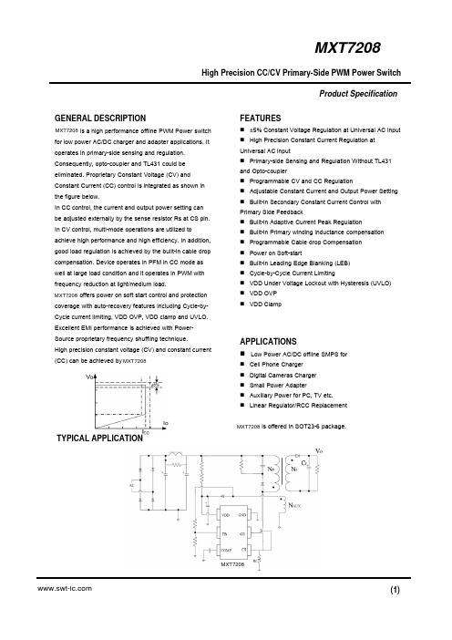
High Precision CC/CV Primary-Side PWM Power SwitchGENERAL DESCRIPTIONis a high performance offline PWM Power switchfor low power AC/DC charger and adapter applications. It operates in primary-side sensing and regulation. Consequently, opto-coupler and TL431 could be eliminated. Proprietary Constant Voltage (CV) and Constant Current (CC) control is integrated as shown in the figure below.In CC control, the current and output power setting can be adjusted externally by the sense resistor Rs at CS pin. In CV control, multi-mode operations are utilized to achieve high performance and high efficiency. In addition, good load regulation is achieved by the built-in cable drop compensation. Device operates in PFM in CC mode as well at large load condition and it operates in PWM with frequency reduction at light/medium load.offers power on soft start control and protectioncoverage with auto-recovery features including Cycle-by-Cycle current limiting, VDD OVP, VDD clamp and UVLO. Excellent EMI performance is achieved with Power-Source proprietary frequency shuffling technique.High precision constant voltage (CV) and constant current (CC) can be achieved by FEATURES⏹±5% Constant Voltage Regulation at Universal AC input ⏹High Precision Constant Current Regulation at Universal AC input⏹Primary-side Sensing and Regulation Without TL431 and Opto-coupler⏹Programmable CV and CC Regulation⏹Adjustable Constant Current and Output Power Setting ⏹Built-in Secondary Constant Current Control with Primary Side Feedback⏹Built-in Adaptive Current Peak Regulation ⏹Built-in Primary winding inductance compensation ⏹Programmable Cable drop Compensation ⏹Power on Soft-start⏹Built-in Leading Edge Blanking (LEB)⏹Cycle-by-Cycle Current Limiting⏹VDD Under Voltage Lockout with Hysteresis (UVLO)⏹VDD OVP ⏹VDD ClampAPPLICATIONS⏹Low Power AC/DC offline SMPS for⏹Cell Phone Charger ⏹Digital Cameras Charger ⏹Small Power Adapter⏹Auxiliary Power for PC, TV etc.⏹Linear Regulator/RCC Replacementis offered in SOT23-6 package.Product SpecificationTYPICAL APPLICATIONMXT7208MXT7208MXT7208MXT7208MXT7208High Precision CC/CV Primary-Side PWM Power SwitchPin ConfigurationThe pin map is shown as below for SOT23-6.Absolute Maximum RatingsProduct SpecificationTERMINAL ASSIGNMENTSGENERAL INFORMATIONPin Num.Pin Name I/O Description 1GND P Ground 2GD O Drive MOSFET 3CS I Current sense input4FB I Feedback5COMP I Loop Compensation for CV Stability6VDD P Power SupplyBLOCK DIAGRAMHigh Precision CC/CV Primary-Side PWM Power SwitchELECTRICAL CHARACTERISTICSProduct Specification(TA = 25C, VDD=VDDG=16V, if not otherwise noted)1. Freq_Max indicates IC internal maximum clock frequency. In system application, the maximum operation frequency of 60Khz nominal occurs at maximum output power or the transition point from CV to CC.Note:High Precision CC/CV Primary-Side PWM Power SwitchProduct Specification CHARACTERIZATION PLOTSHigh Precision CC/CV Primary-Side PWM Power Switch OPERATION DESCRIPTIONProduct Specificationis a cost effective PWM power switch optimized for off-line low power AC/DC applications including battery chargers and adapters. It operates in primary side sensing and regulation, thus opto-coupler andTL431 are not required. Proprietary built-in CV and CC control can achieve high precision CC/CV control meeting most adapter and charger application requirements.● Startup Current and Start up ControlStartup current of is designed to be very low so that VDD could be charged up above UVLO threshold and starts up quickly. A large value startup resistor can therefore be used to minimize the power loss in application.● Operating CurrentThe Operating current of is as low as 2.5mA. Good efficiency is achieved with the low operating current together with ‘Muti-mode’ control features.● Soft Startfeatures an internal soft start to minimize the component electrical over-stress during power on startup. As soon as VDD reaches UVLO (OFF), the control algorithm will ramp peak current voltage threshold gradually from nearly zero to normal setting of 0.90V. Every restart is a soft start.● CC/CV Operationis designed to produce good CC/CV control characteristic as shown in the Fig. 1. In charger applications, a discharged battery charging starts in the CC portion of the curve until it is nearly full charged and smoothly switches to operate in CV portion of the curve. In an AC/DC adapter, the normal operation occurs only on the CV portion of the curve. The CC portion provides output current limiting. In CV operation, the output voltage is regulated through the primary side control. In CC operation mode, will regulate the output current constant regardless of the output voltage drop.● Principle of OperationTo support proprietary CC/CV control, system needs to be designed in DCM mode for flyback system (Refer to Typical Application Diagram on page1). In the DCM flyback converter, the output voltage can be sensed via the auxiliary winding. During MOSFET turn-on time, the load current is supplied from the output filter capacitor Co. The current in the primary winding ramps up. When MOSFET turns off, the primary current transfers to the secondary at the amplitude ofThe auxiliary voltage reflects the output voltage as shown in fig.2 and it is given byWhere ΔV indicates the drop voltage of theoutput Diode.Fig.2. Auxiliary voltage waveformVia a resistor divider connected between the auxiliary winding and INV (pin 3), the auxiliary voltage is Sampled at the end of the demagnetization and it is hold until the next sampling. The sampled voltage is compared with Vref(2.0V) and the error is amplified. The error amplifier output COMP reflects the load condition and controls the PWM switching frequency to regulate the output voltage, thus constant output voltage can be achieved.When sampled voltage is below Vref and the error amplifier output COMP reaches its maximum, the switching frequency is controlled by the sampled voltage thus the output voltage to regulate the output current, thus the constant output current can be achieved.● Adjustable CC point and Output PowerIn , the CC point and maximumoutput power can be externally adjusted by external current sense resistor Rs at CS pin as illustrated in Typical Application Diagram. The output power is adjusted through CC point change. The larger Rs, the smaller CC point is, and the smaller output power becomes, and vice versaas shown in Fig.3.MXT7208MXT7208MXT7208MXT7208MXT7208MXT7208MXT7208MXT7208High Precision CC/CV Primary-Side PWM Power SwitchProduct Specification●Operation switching frequencyThe switching frequency of is adaptively controlled according to the load conditions and the operation modes. No external frequency setting components are required. The operation switching frequency at maximum output power is set to 60KHz internally.For flyback operating in DCM, The maximum output power is given byWhere Lp indicate the inductance of primary winding and Ip is the peak current of primary winding.Refer to the equation 3, the change of the primary winding inductance results in the change of the maximum output power and the constant output current in CC mode. To compensate the change from variations of primary winding inductance, the switching frequency is locked by an internal loop such that the switching frequency isSince TDemag is inversely proportional to the inductance, as a result, the product Lp and fsw is constant, thus the maximum output power and constant current in CC mode will not change as primary winding inductance changes. Up to ±10% variation of the primary winding inductance can be compensated. Frequency shuffling for EMIimprovement The frequency shuffling (switching frequency modulation) is implemented in . The oscillation frequency is modulated so that the tone energy is spread out. The spread spectrum minimizes the conduction band EMI and therefore eases the system design.● Current Sensing and Leading Edge BlankingCycle-by-Cycle current limiting is offered incurrent mode PWM control. The switch current isdetected by a sense resistor into the CS pin. An internal leading edge blanking circuit chops off the sensedvoltage spike at initial internal power MOSFET on state so that the external RC filtering on sense input is no longer needed. The PWM duty cycle is determined by the current sense input voltage and the EA output voltage.● Gate DriveThe internal power MOSFET in is driven by adedicated gate driver for power switch control.Too weak the gate drive strength results in higher conduction and switch loss of MOSFET while too strong gate drivecompromises EMI.A good tradeoff is achieved through the built-in totem pole gate design with right output strength control.● Programmable Cable drop Compensation In , cable drop compensation is implemented to achieve good load regulation. An offset voltage isgenerated at INV by an internal current flowing into the resister divider. The current is inversely proportional to the voltage across pin COMP, as a result, it is inversely proportional to the output load current, thus the drop due to the cable loss can be compensated.As the load current decreases from full-load to noload,the offset voltage at INV will increase. It can also be programmed by adjusting the resistance of the divider to compensate the drop for various cable lines used.● Protection ControlGood power supply system reliability is achieved with its rich protection features including Cycle-by-Cycle current limiting (OCP), VDD clamp, Power on Soft Start, and Under Voltage Lockout on VDD (UVLO).VDD is supplied by transformer auxiliary winding output.The output of is shut down when VDD dropsbelow UVLO (ON) limit and Switcher enters power onstart-up sequence thereafter.MXT7208MXT7208MXT7208MXT7208MXT7208MXT7208High Precision CC/CV Primary-Side PWM Power SwitchProduct Specification PACKAGE MECHANICAL DATASOT23-6。

Rev. 1.3012021-08-18HT77xxBA5V/200mA PFM异步升压转换器特性•低启动电压:0.85V (典型值) •效率高达85% •超低空载输入电流•高输出电压精度:±2.5%•固定输出电压:2.7V/3.0V/3.3V/3.7V/5.0V •超低关机电流:0.1μA (典型值) •封装类型:3-pin SOT23、5-pin SOT23、3-pin SOT89应用领域•单节、双节、三节碱性/ NiMH / NiCd 电池供电的便携式产品 •便携式装置/手持式设备概述HT77xxBA 系列为PFM 升压DC/DC 转换器,效率高、纹波低。
此系列具有超低启动电压以及高输出电压精度。
仅需少量外部元器件便可提供固定的2.7V/3.0V/3.3V/ 3.7V/5.0V 输出电压。
CMOS 技术确保低电源电流,使得该系列芯片成为单节或多节电池供电应用的理想选择。
HT77xxBA 系列内置一个振荡器、一个PFM 控制电路、一个驱动晶体管、一个参考电压单元以及一个高速比较器。
采用脉冲频率调制(PFM)可实现轻载输出时电源电流以及纹波尽可能小。
这些芯片采用节省空间的3-pin SOT89、3-pin SOT23和5-pin SOT23封装类型。
5-pin SOT23封装包含芯片使能功能,在关机模式时可减小功耗。
典型应用电路V V OUT选型表注:“xx ”表示输出电压。
Rev. 1.3022021-08-18LXOUTGND引脚图CEOUTNCSOT23-5GNDOUTLXSOT89GNDLXSOT23引脚说明建议工作范围注:极限参数表示超过此界限可能将对芯片造成损害。
建议工作范围表示芯片可正常工作的条件,但不包含特定限制条件。
Rev. 1.3032021-08-18Rev. 1.3042021-08-18V IN =0.6×V OUT ,I OUT =10mA ,Ta=25˚C,除非另有说明注:极限参数表示超过此界限可能将对芯片造成损害。

RT4720ATriple DC/DC Boost Converter for AMOLEDGeneral DescriptionRT4720A is a triple channels DC/DC converter which is designed to provide the power of AMOLED. It integrates step up DC/DC and an inverting converter to provide the positive and negative output voltage required by AMOLED.For the portable application, board space and efficiency are always major concerns. The high switching frequency of RT4720A allows the use of low inductance inductor to save the board space. It provides dual positive output voltage, one is a fixed 5.8V or 7.7V output voltage by SEL pin and the other positive output is fixed 4.6V. For the negative output voltage, it can be programmed by external MCU through single wire (SWIRE pin). The output voltage range of negative output voltage is -1.4V to -5.4V. RT4720A has OTP, SCP, UVLO and over current protections. The RT4720A is available in a WQFN -16L 3x3 package to achieve saving PCB space.Features●Boost Converter to Supply Positive AVDD Voltage Fixed 5.8V or 7.7V●Boost Converter to Supply AMOLED Positive Voltage 4.6V●Inverter Converter to Supply AMOLED Negative Voltage From -1.4V to -5.4V● Maximum Output Current up to 300mA for AMOLED Positive & Negative Power Supply●Maximum Output Current up to 50mA for Fixed 5.8V or 7.7V AVDD Output Voltage● Typical Peak Efficiency : 90% (40mA to 150mA) ● ********************************● High Output Voltage Accuracy ● Excellent Line and Load Transient ● Excellent Line and Load Regulation● Programmable Negative Voltage by SWIRE Pin ● Fast Outputs Discharge Function● Low Quiescent Current <1 A in Shutdown Mode ● Internal Soft Start to limit Inrush Current ● Over Temperature Protection (OTP) ● Over Current Protection (OCP) ●Short Circuit Protection (SCP)Applications● Cellular Phones ● Digital Cameras ● PDAs and Smart Phones ●Probable InstrumentSimplified Application CircuitVBAT V POSAVDD V NEGRT4720AOrdering InformationPackage TypeQW : WQFN-16L 3x3RT4720ALead Plating SystemG : Green (Halogen Free and Pb Free)Note :Richtek products are :④ RoHScompliant and compatible with the current requirements of IPC/JEDEC J-STD-020.④ Suitablefor use in SnPb or Pb-free solderingprocesses.Marking Information7Y= : Product Code YMDNN : Date CodePin Configurations(TOP VIEW)A V I N P G N D 2L X 3S E L LX1PGND1FBSLX2V O 3PVIN VO2N C E N O 3A G N D VO1SWIRE1211109131415161234876517AGNDWQFN-16L 3x3Functional Pin DescriptionRT4720AFunctional Block DiagramOperationThe RT4720A is a triple channels DC/DC converter which is designed to provide the power of AMOLED that can support the input voltage range from 2.9V to 4.5V. The VO1&VO2 output current can be up to 300mA, and the VO3 output current can be up to 50mA. The RT4720A uses current mode architecture for the purpose of high efficiency and high transient response. The VO1 positive output voltage is produced from the DC/DC Boost converter and is set at a typical value of 4.6V. When the SWIRE goes high, the positive output voltage will be enabled with an internal soft-start process. The VO2 negative output voltage is produced from the DC/DC Buck-Boost converter and the negative output voltage range is -1.4V to -5.4V. It can be programmed by external MCU through single wire (SWIRE pin). The VO3 positive output voltage is produced from the DC/DC Boost converter and is set at a fixed 7.7V or 5.8V by SEL pin. When SWIRE goes high and VO1 soft-start had finished already, negative output voltage VO2 will be enabled with an internal soft-start process.RT4720ATable 1. SWIRE Command LUT for VO2Table 2. SWIRE Pin CharacteristicsRT4720ATiming DiagramSWIRE Command Timing DiagramT en_dly< 400μs2μs < T off < 20μsPower SequenceT off_dly > 300μsRT4720AT> 300 sRT4720A Absolute Maximum Ratings(Note 1)●PVIN, AVIN, VO1, LX1, FBS, SEL, ENO3, SWIRE ----------------------------------------------------------- -0.3 to 6V●VO3, LX3 ---------------------------------------------------------------------------------------------------------------- -0.3 to 12V●VO2 ----------------------------------------------------------------------------------------------------------------------- -6 to 0.3V●LX2 ------------------------------------------------------------------------------------------------------------------------ -6 to 6V●Power Dissipation, P D @ T A = 25︒CWQFN-16L 3x3 -------------------------------------------------------------------------------------------------------- 3.33W●Package Thermal Resistance (Note 2)WQFN-16L 3x3, θJA -------------------------------------------------------------------------------------------------- 30︒C/WWQFN-16L 3x3, θJC -------------------------------------------------------------------------------------------------- 7.5︒C/W●Lead Temperature (Soldering, 10 sec.) -------------------------------------------------------------------------- 260︒C●Junction Temperature ------------------------------------------------------------------------------------------------ 150︒C●Storage Temperature Range --------------------------------------------------------------------------------------- -65︒C to 150︒C ●ESD Susceptibility (Note 3)HBM (Human Body Model) ----------------------------------------------------------------------------------------- 2kVMM (Machine Model) ------------------------------------------------------------------------------------------------- 200V Recommended Operating Conditions (Note 4)●Supply Input Voltage ------------------------------------------------------------------------------------------------- 2.9V to 4.5V●Ambient Temperature Range--------------------------------------------------------------------------------------- -40︒C to 85︒C ●Junction Temperature Range -------------------------------------------------------------------------------------- -40︒C to 125︒C Electrical Characteristics(V IN = 3.7V, V O1 = 4.6V, V O2 = -4V, V O3 = 7.7V, T A = 25︒C, unless otherwise specified)RT4720ART4720A Note 1. Stresses beyond those listed “Absolute Maximum Ratings” may cause permanent damage to the device. These are stress ratings only, and functional operation of the device at these or any other conditions beyond those indicated in the operational sections of the specifications is not implied. Exposure to absolute maximum rating conditions may affect device reliability.Note 2. θJA is measured at T A= 25︒C on a high effective thermal conductivity four-layer test board per JEDEC 51-7. θJC is measured at the exposed pad of the package.Note 3. Devices are ESD sensitive. Handling precaution recommended.Note 4. The device is not guaranteed to function outside its operating conditions.RT4720ATypical Application CircuitVBAT V POS(Fixed 4.6V)AVDD (5.8V & 7.7V)V NEGTable 3. Typical BOM ListTypical Operating CharacteristicsVO1&VO2 Efficiency vs. Load Current707580859095100E f f i c i e n c y (%)VO3 Efficiency vs. Load Current6065707580859095100E f f i c i e n c y (%)4.564.574.584.594.604.614.624.634.64V P O S V o l t a g e (V )VNEG Voltage vs. Load Current-4.04-4.03-4.02-4.01-4.00-3.99-3.98-3.97-3.9600.050.10.150.20.250.3Load Current (A)V N E G V o l t a g e (V )7.667.677.687.697.707.717.727.737.7401020304050Loader Current (mA)A V D D V o l t a g e (V )V IN = 3.7VSWIRE (2V/Div)VO1(2V/Div)VO2(2V/Div)I IN(500mA/Div)Time (1ms/Div)VO1 & VO2 Power OnVO1 & VO2 Power OffTime (1ms/Div)SWIRE (2V/Div)VO1(2V/Div)VO2(2V/Div)I IN(500mA/Div)V IN = 3.7VVO3 Power OnTime (1ms/Div)VIN (2V/Div)ENO3(2V/Div)VO3(3V/Div)I IN(500mA/Div)V IN = 3.7VVO3 Power OffTime (1ms/Div)V IN = 3.7VVIN (2V/Div)ENO3(2V/Div)VO3(3V/Div)I IN(500mA/Div)Application InformationThe RT4720A is a triple channels DC/DC converter, which integrates dual step up converter and an inverting converter to provide the positive and negative output voltage required by AMOLED. RT4720A protection function includes Over Temperature Protection (OTP), Over Current Protection (OCP) and Short Circuit Protection (SCP), also it has Pulse Skipping Mode (PSM) to provide high efficiency during light load.Soft-StartThe RT4720A use an internal soft-start feature to avoid high inrush currents during step-up.Fast Discharge FunctionAll outputs voltage use an embedded discharge function to discharge the remaining output to 0V rapidly, preventing phenomena such as residual image on the display during shutdown.Over Temperature Protection (OTP)The RT4720A includes an Over Temperature Protection (OTP) feature to prevent excessive power dissipation from overheating the device. The OTP will shut down switching operation when junction temperature exceeds 140︒C. Once the junction temperature cools down by approximately 15︒C, the converter resumes operation.To maintain continuous operation, prevent the maximum junction temperature from rising above 125︒C.Over Current Protection (OCP)The RT4720A includes a current sensing circuitry which monitors the inductor current during each ON period. If the current value becomes greater than the current limit, the switch that pertains to inductor charging will turn off, forcing the inductor to leave charging stage and enter discharge stage.Short Circuit Protection (SCP)The RT4720A has an advanced short circuit protection mechanism which prevents damage to the device from unexpected applications. When the output voltage becomes lower than about 90%, over 1ms the device enters shutdown mode. VO3 can only re-start normal operation after triggering the ENO3 pin and VO1, VO2 can only re-start normal operation after triggering the SWIRE pin.Under Voltage Lockout (UVLO)To prevent abnormal operation of the IC in low voltage condition, an under voltage lockout is included, which shuts down the device at voltages lower than 2.2V. All functions will be turned off in this state.Input Capacitor SelectionEach channel input ceramic capacitors with 10μF capacitance are suggested for the RT4720A applications. However, to achieve best performance with the RT4720A, larger capacitance can be used. For better voltage filtering, select ceramic capacitors with low ESR, X5R and X7R types which are suitable because of their wider voltage and temperature ranges.Boost Inductor SelectionThe inductance depends on the maximum input current. As a general rule, the inductor ripple current range is 20% to 40% of the maximum input current. If 40% is selected as an example, the inductor ripple current can be calculated according to the following equations :OUT OUT(MAX)IN(MAX)INL IN(MAX)V II=ηVΔI= 0.4I⨯⨯⨯where η is the efficiency of the converter, I IN(MAX) is the maximum input current, and ΔI L is the inductor ripple current. The input peak current can then be obtained by adding the maximum input current with half of the inductor ripple current as shown in the following equation :I PEAK = 1.2×I IN(MAX)Note that the saturated current of the inductor must be greater than I PEAK.The inductance can eventually be determined according to the following equation :()()()2IN OUT IN2OUT OUT(MAX)OSCηV V-VL =0.4V I f⨯⨯⨯⨯⨯where f OSC is the switching frequency. For better system performance, a shielded inductor is preferred to avoid EMI problems.Boost Output Capacitor SelectionThe output ripple voltage is an important index for estimating chip performance. This portion consists of two parts. One is the product of the inductor peak current with the ESR of the output capacitor, while the other part is formed by the charging and discharging process of the output capacitor. As shown in Figure 1, ΔV OUT1 can be evaluated based on the ideal energy equalization. According to the definition of Q, the Q value can be calculated as the following equation :IN L OUT IN L OUT IN OUT OUT1OUT OSC111Q = I +ΔI -I +I -ΔI -I 222V 1= C V V f ⎡⎤⎛⎫⎛⎫⨯ ⎪ ⎪⎢⎥⎝⎭⎝⎭⎣⎦⨯⨯⨯where f OSC is the switching frequency and ΔI L is the inductor ripple current. Bring C OUT to the left side to estimate the value of ΔV OUT1 according to the following equation :OUTOUT1ESR OUT OSCD I ΔV = ΔV +ηC f ⨯⨯⨯where ESR C C_ESR PEAK C_ESR ΔV = ΔI R = I R ⨯⨯The output capacitor, C OUT , should be selected accordingly.Figure 1. The Output Ripple Voltage without theContribution of ESRAVDD Output Voltage SettingThe AVDD boost output voltage VO3 is fixed 7.7V or 5.8V output voltage by SEL pin. When SEL pin is set to high, the output voltage is 5.8V or otherwise SEL pin is set to low, the output voltage is changed to 7.7V.Buck-boost Converter Inductor SelectionThe first step in the design procedure is to verify whether the maximum possible output current of the buck-boost converter supports the specific application requirements. To simply the calculation, the fastest approach is to estimate converter efficiency by taking the efficiency numbers from provided efficiency curves or to use a worst case assumption for the expected efficiency, e.g., 80%. The calculation must be performed for the minimum assumed input voltage where the peak switch current is the highest. The inductor has an internal switch to be able to handle this current.④Converter Duty Cycle :OUT IN OUT-V D =V η-V ⨯④Maximum output current :()IN OUT PEAK OSC V D I = I -1-D 2f L ⎛⎫⨯⨯ ⎪⨯⨯⎝⎭④Inductor peak current :OUT IN PEAK OSC I V DI =+1-D 2f L⨯⨯⨯ As for inductance, we are going to derive the transition point, where the converter toggles from CCM to DCM. We need to define the point at which the inductor current ripple touches zero, and as the power switch SW is immediately reactivated, the current ramps up again. Figure 2 portrays the input current activity of the buck-boost converter.Figure 2. The Buck-Boost Input Signature in BCM The inductance can eventually be determined according to the following equation :2OUT INcritical OSC OUT IN OUTV ηV L = 2f I V +V ⎛⎫⨯⨯⎪ ⎪⨯⨯⎝⎭Buck-Boost Converter Output Capacitor Selection For the best output voltage filtering, low ESR ceramic capacitors are recommended. One 10μF output capacitors with sufficient voltage ratings in parallel are adequate for most applications. Additional capacitors can be added to improve load transient response. To calculate the output voltage ripple, the following equations can be used :OUT ESR OSC LOAD OUTD V ΔV =+ΔV f R C ⨯⨯⨯where ESR C C_ESR PEAK C_ESR ΔV = ΔI R = I R ⨯⨯ΔV ESR can be neglected in many cases since ceramic capacitors provides very low ESR.Negative Output Voltage SettingBuck-boost converter is implementing a pulse dimming method to control the output voltage (VO2) and its value is from -1.4V to -5.4V in 0.1V increments. User can control VO2 by SWIRE command. See SWIRE command section for details on how to adjust the output voltage.Thermal ConsiderationsFor continuous operation, do not exceed absolute maximum junction temperature. The maximum power dissipation depends on the thermal resistance of the IC package, PCB layout, rate of surrounding airflow, and difference between junction and ambient temperature. The maximum power dissipation can be calculated by the following formula : P D(MAX) = (T J(MAX) - T A ) / θJAwhere T J(MAX) is the maximum junction temperature, T A is the ambient temperature, and θJA is the junction to ambient thermal resistance.For recommended operating condition specifications, the maximum junction temperature is 125︒C. The junction to ambient thermal resistance, θJA , is layout dependent. For WQFN-16L 3x3 package, the thermal resistance, θJA , is 30︒C/W on a standard JEDEC 51-7 four-layer thermal test board. The maximum power dissipation at T A = 25︒C can be calculated by the following formula :P D(MAX) = (125︒C - 25︒C) / (30︒C/W) = 3.33W for WQFN-16L 3x3 packageThe maximum power dissipation depends on the operating ambient temperature for fixed T J(MAX) and thermal resistance, θJA . The derating curve in Figure 3 allows the designer to see the effect of rising ambient temperature on the maximum power dissipation.Figure 3. Derating Curve of Maximum PowerDissipationLayout ConsiderationFor the best performance of RT4720A, thefollowing PCB layout guidelines should be strictly followed.④ For good regulation, place the power components asclose to the IC as possible. The traces should be wide and short, especially for the high current output loop.④ The input and output bypass capacitor should be placed as close to the IC as possible and connected to the ground plane of the PCB.④ Minimize the size of the LX1, LX2, LX3 nodes andkeep the traces wide and short. Care should be taken to avoid running traces that carry any noise-sensitive signals near LX or high-current traces.④ Separate power ground (PGND) and analog ground (AGND). Connect the AGND and the PGND islands at a single end. Make sure that there are no otherconnections between these separate ground planes. ④ Connect the exposed pad to a strong ground planefor maximum thermal dissipation.0.00.40.81.21.62.02.42.83.23.64.00255075100125Ambient Temperature (°C)M a x i m u m P o w e r D i s s i p a t i o n (W )Figure 4. PCB Layout GuideOutline DimensionW-Type 16L QFN 3x3 PackageRichtek Technology Corporation14F, No. 8, Tai Yuen 1st Street, Chupei CityHsinchu, Taiwan, R.O.C.Tel: (8863)5526789Richtek products are sold by description only. Richtek reserves the right to change the circuitry and/or specifications without notice at any time. Customers should obtain the latest relevant information and data sheets before placing orders and should verify that such information is current and complete. Richtek cannot assume responsibility for use of any circuitry other than circuitry entirely embodied in a Richtek product. Information furnished by Richtek is believed to be accurate and reliable. However, no responsibility is assumed by Richtek or its subsidiaries for its use; nor for any infringements of patents or other rights of third parties which may result from its use. No license is granted by implication or otherwise under any patent or patent rights of Richtek or its subsidiaries.。
盛扬推出升压型DC/DC转换器HT77XX
无
【期刊名称】《电子测试:新电子》
【年(卷),期】2005(000)004
【摘要】盛扬半导体日前推出高效率升压型DC/DC转换器HT77XX,该转换器利用CMOS工艺以及PFM、(Pulse Frequency Modulation)技术,呈现低功耗及低噪声特性。
通过集成一个低阻抗的功率晶体管,HT77XX仅需外接电感、电容及二极管等三个元器件,就可以组成一个效率高达85%的DC/DC转换电路,是低成本、省空间的升压解决方案。
【总页数】1页(P100)
【作者】无
【作者单位】无
【正文语种】中文
【中图分类】TM4
【相关文献】
1.凌力尔特推出具双输入电源通路控制的同步降压-升压型DC/DC转换器 [J],
2.凌力尔特推出双通道DC/DC转换器用于有源矩阵OLED和CCD偏置的升压型和负输出DC/DC转换器 [J],
3.盛群新发布超低激活电压的升压型DC/DC转换器——HT77XX [J],
4.Linear推出1.5A同步降压型DC/DC转换器,2MHz提供93%效率 [J],
5.盛群半导体新推出超低启动电压的升压型DC/DC转换器 [J],
因版权原因,仅展示原文概要,查看原文内容请购买。
Application Note: SY7728F60V High Efficiency Four-String Boost LED DriverGeneral DescriptionSY7728F is a high efficiency peak current mode boost controller with four matching current sources to drive WLED arrays of LCD backlight.The device has a wide input voltage range from 4.5V to 30V. The LED current is programmable through a resistor. It also integrates both PWM and Analog dimming function for accurate LED current control.Ordering InformationPackage Code Temperature Code Optional Spec Code□(□□)□SY7728Features∙ 4.5-30V Wide Input Voltage Range∙Programmable 5mA~240mA LED Current per String∙LED Current with +/-3% Accuracy at 100mA per String∙PWM and Analog Mode Dimming: Dimming Frequency: 100Hz~50 kHz∙+/-1% Current Matching Among Strings at 100mA per String∙Programmable Switching Frequency,100kHz-1MHz ∙Internal Soft-start∙Open and Short LED Protection∙Programmable over-voltage Protection ∙RoHS Compliant and Halogen Free ∙Compact Package: SOP16E&SOP16Applications∙Monitor Panel Backlight ∙TV Panel BacklightTypical ApplicationsFigure 1. Typical Application CircuitPWM, 100Hz-SY7728F REFERENCE APPLICATION CIRCUIT-PARALLEL OPERATIONPinout (top view)CADIM LED1LED2LED3LED4RT EN ISET VCCPWM INISEN OVP GND COMP GATECADIM LED1LED2LED3LED4RT EN ISET VCCPWM INISEN OVP GND COMP GATE (SOP16E) (SOP16)Top Mark: CBP xyz for SY7728FFEC (Device code: CBP; x=year code, y=week code, z= lot number code )CBG xyz for SY7728FFFC (Device code: CBG; x=year code, y=week code, z= lot number code)Function BlockISENRTCADIMENPWMISETVCC GATE GNDLED1 LED4COMPOVPINAbsolute Maximum Ratings(Note 1)LED x--------------------------------------------------------------------------------------------------------------- -0.3 to 60VIN, EN,CA DIM--------------------------------------------------------------------------------------------------- -0.3 to 33VGate, VCC------------------------------------------------------------------------------------ -0.3 to min(15V, VIN+0.3V) All other p ins-------------------------------------------------------------------------------------------------------- -0.3 to 6VPower Dissipation, PD @ TA = 25°C SOP16E/SOP16---------------------------------------------------------------------2.5WPackage Thermal Resistance (Note 2)SOP16EθJA--------------------------------------------------------------------------------------- 40°C/W SOP16E θJC ----------------------------------------------------------------------------------------------------------- 20°C/W SOP16 θJA ----------------------------------------------------------------------------------------------------------- 80°C/W SOP16 θJC--------------------------------------------------------------------------------------- 18°C/W Junction Temperature Range -----------------------------------------------------------------------------------------150°CLead Temperature (Soldering, 10 sec.) ---------------------------------------------------------------------------- 260°CStorage Temperature Range ---------------------------------------------------------------------------- -65°C to 150°C Recommended Operating Conditions(Note 3)Supply Input Voltage ------------------------------------------------------------------------------------------------- 4.5V to 30V Junction Temperature Range ----------------------------------------------------------------------------------- -40°C to 125°C Ambient Temperature Range ------------------------------------------------------------------------------------ -40°C to 85°CElectrical CharacteristicsNote 1:Stresses beyond the “Absolute Maximum Ratings” may cause permanent damage to the device. These are stress ratings only. Functional operation of the device at these or any other conditions beyond those indicated in the operatio nal sections of the specification is not implied. Exposure to absolute maximum rating conditions for extended periods may affect device reliability.Note 2:θJA is measured according to JESD51-2, 51-7 while ambient temperature=25℃, θJC is measured in accordance with JESD51-14.Note 3: The device is not guaranteed to function outside its operating conditions.Note 4: This parameter is guaranteed by design.Note 5: The recommended minimum PWM on time is 1µs.Typical Performance Characteristics (V IN =12V, I LED =100mA, 54V per string, 4 strings )I L E D (m A )Analog Dimming CurveAnalog Dimming Duty Cycle (%)102030405060708090100I L E D (m A)PWM Dimming Duty Cycle (%)102030405060708090100Analog PWM Dimming(f ADIM =100Hz, d=50%)Time (2ms/div and 1µs/div)PWM 5V/divV OUT 50V/div V DRAIN 50V/div I LED50mA/divPWM Dimming(f ADIM =100Hz, d=50%)Time (2ms/div and 1µs/div)PWM 5V/div V OUT 50V/div V DRAIN 50V/div I LED100mA/divAnalog PWM Dimming(f ADIM =50kHz, d=50%)Time (5μs/div)PWM5V/divV OUT 50V/div V DRAIN 50V/div I LED 50mA/div PWM Dimming(f ADIM =50kHz, d=50%)Time (5μs/div)PWM5V/divV OUT 50V/divV DRAIN 50V/divI LED 100mA/divStartup from V INTime (10ms/div)V IN 10V/div V OUT 50V/div V DRAIN50V/divI LED100mA/divStartup from ENTime (10ms/div)EN 2V/div V OUT50V/divV DRAIN50V/divI LED100mA/divSteady StateTime (5μs/div)PWM 5V/div V COMP1V/divV DRAIN50V/divI LED 100mA/divOpen LED Protection (Open LED2)Time (10ms/div and 1µs/div)V LX50V/div I LED1100mA/divV OUT 20V/div V LED1 2V/div LED20.2V/div V OUT 20V/div V DRAIN50V/div I LED100mA/divApplications InformationThe SY7728F contains a peak current mode boost controller and 4-channel matching current sources to drive WLED arrays of LCD backlight. The device works under programmable switching frequency. The internal soft-start function avoids the inrush current during startup. Refer to the block diagram to better understand the operation of the IC.LE D Current Setting:LED1~LED4 are the 4-channel LED driver outputs. The sinking current of each channel can be programmed with a resistor R ISET connecting from ISET pin to ground:pwmLED=SET =ISET pwm DOWN LED=SET =ISET DOWN 1200D I I (mA)(PWM)R (Kohm)1200D R I I (mA)(Ana log)R (R +50)(Kohm)⨯⨯⨯⨯For PWM mode R ISET =10K Ω(ohm), the LED current is set to 120mA. The maximum sinking current of each channel is 240mA. For higher current application, different channels can be paralleled. The LED current evenly flow through the paralleled channels because of good current matching.Input Capacitor CIN:The ripple current through input capacitor is calculated as:IN OUT IN CIN_RMS I =X5R or X7R ceramic capacitors with greater than 4.7uF capacitance are recommended to handle this ripple current. To minimize the potential noise problem, place this ceramic capacitor really close to the IN and GND pins. Care should be taken to minimize the loop area formed by C IN , and IN/GND pins.Output Capacitor C OUT :The output capacitor is selected to handle the output ripple noise requirements. This ripple voltage is related to the capacitor’s capacitance and its equivalent series resistance (ESR). For the best performance, it is recommended to use X5R or better grade low ESR ceramic capacitor. The voltage rating of the output capacitor should be higher than the maximum output voltage. The minimum required capacitance can be calculated as:LED OUT IN OUT SW OUT RIPPLEn I (V V )C F V V ⨯⨯-=⨯⨯RIPPLEV is the peak to peak output ripple, n is thenumber of LED string.For LED applications, the output capacitance should be large enough to attenuate the V LEDX ripple voltage. Formost applications, a 4.7μF ceramic capacitor in parallel with a 47uF electrolytic capacitor will be sufficient. Inductor L:There are several considerations in choosing this inductor. 1)Choose the inductance to provide the desired ripplecurrent. The inductance is calculated as:L =V inV out2×V out −V in ×ηn ×I led ×F sw ×∆I LI L(for CCM )Where F SW is the switching frequency, n is the number ofLED string , I LED i s the current of each LED string,Vin is input voltage,Vout is output voltage ,Δ is total inductor current ripple, is inductor average current. 2)The saturation current rating of the inductor must be selected to be greater than the peak inductor current under full load conditions.Where is total efficiency.3)The DCR of the inductor and the core loss at the switching frequency must be low enough to achieve the desired efficiency requirement.Main MOSFE T Selection:The choice of the main MOSFET depends on the current through MOSFET, the maximum V DS voltage, the switching frequency, the capability of the MOSFET to dissipate heat.The maximum RMS current through MOSFET is given by:I mos _rms =V out ×n ×I ledV in ×ηV out −V in V out 1+13(∆I L 2×I L)2(for CCM )The maximum drain to source voltage equals the outputvoltage.Rectifier Diode Selection:Because of high switching speed of SY7728F, a Schottky diode with low forward voltage drop and fast switching speed is desirable for the application. The voltage rating of the diode must be higher than maximum output voltage. T he diode’s average and peak current rating should exceed the average output current and peak inductor current.Internal 10V LDO:VCC is the output of internal LDO. Connect a 1uF capacitor from VCC pin to ground. This LDO provides 10V power supply for the external MOSFET gate driver. The typical dropout voltage of the LDO is 200mV. VCC drops to 0 when the IC shuts down.Open LE D Protection:When any LED string is open, the respective LEDx pin will be pulled to ground. SY7728F continues charging the output voltage until over voltage protection is triggered. Then the part stops switching and checks the condition of all the LEDx pins. The part will mark off and disable the one which voltage is below 100mV. Then the output of boost slowly drops because of the load current. The IC resumes switching once the V OUT goes back to the regulation value. When all LED strings are open, over voltage protection is triggered, the IC will turn off the boost converter.Short LE D Protection:When any diode on the LED string becomes shorted, the LEDx voltage on that string may exceed V SCP_TH (typical 8V), and short LED fault is detected. If short LED fault lasts for more than 15mS (typical value), the IC will mark off and disable that string. When all strings are marked off, the IC will also latch off the boost converter. Recycling input power or enable signal to turn on the disabled string after fault condition is removed.No Rectifier Diode Protection:When the chip is enabled, SY7728F will check the connection of the rectifier diode by sensing the voltage on OVP pin. If the voltage on OVP pin is lower than V OSP_TH (typical 40mV), the IC will shut down.Peak Current Limitation:The device employs cycle by cycle current limitation to protect the main FET of Boost circuit. When the peak current sensing voltage (V ISEN) exceeds 480mV (typical value), the device will turn off the main FET. The FET will turn on again until next clock signal arrives.Diode/Inductor Short-Circuit Protection:When Diode/Inductor Short is happened, the current flow through Boost MOSFET will increase significantly. If the voltage on ISEN pin exceeds approximately 0.58V during the ON period of the boost MOSFET. If the short last for about 15ms during PWM on time, The IC will shut off and stay latched after timer expires. Timer will be reset if ISEN pin voltage drops below 0.58V for eight (8) consecutive clock cycles.Over Temperature Protection:To prevent the IC from over temperature, the device will shutdown when the junction temperature exceeds 150℃. When the junction temperature decrease to 130 ℃,IC will resume to switching.Abnormal Working when VIN>VLED:If VIN>LED Forward Voltage at EN on, which may cause VLEDX>LED regulation voltage last for about 15ms then the boost converter will be latched off. Need to avoid such application condition.High Output Voltage Application:In applications when the LED string voltage is higher than the maximum voltage rating of LEDx pins, a high voltage rating external MOSFET can be used as shown below to prevent the IC from damage.Multiple Controllers in Parallel Operation:For applications having more than 4 LED strings, designer can use multiple controllers for parallel operation. A reference circuit is illustrated in Figure 2.Both controllers share the common Boost converter power train for 8 strings of LED operation.Layout Design:Proper PCB layout and components placement are critical to the performance of the IC and to prevent noise and electromagnetic interference problems. Following are some rules for the PCB layout:1)The loop of main FET, rectifier diode, and outputcapacitor must be as short as possible2)It is desirable to maximize the PCB copper areaconnecting to GND pin to achieve the best thermal and noise performance. If the board space allowed, a ground plane is highly desirable.3)C IN must be close to Pins IN and GND. The loop areaformed by C IN and GND must be minimized.4)The PCB copper area associated with main FETdrain must be minimized to avoid the potential noise problem.5)The small signal components must be placed close toIC and must NOT be adjacent to the main FET drain net on the PCB layout to avoid the noise problem.6)The GND of ceramic capacitor of C ADIM must beplaced as closed as GND pin (pin 15) to avoid noise interference in analog dimming application.7)Boost rectifier diode/inductor short protection isachieved by detecting the voltage between ISEN pin (pin 6) and GND pin (pin 15).The current is very high when short fault occurs, the trace between the source pole of boost main FET and current sense resistor, the trace between the drain pole of boos t main FET and anode of boost rectifier diode/inductor must be as short and wide as possible.SOP16 Package Outline & PCB Layout0.00Top view Front view.41.5Side viewRecommended PCB layoutNotes:All dimension in millimeter and exclude mold flash & metal burrSOP16E Package Outline & PCB LayoutTop ViewBottom ViewSide View A Side View B Notes: All dimension in millimeter and exclude mold flash & metal burrReel WidthTaping & Reel Specification1.Taping orientationFeeding direction2.Carrier Tape & Reel specification for packages3.Others: NARevision HistoryThe revision history provided is for informational purpose only and is believed to be accurate, however, not warranted.。
Wide input voltage,non-isolated ®ulated single outputRoHSFEATURES●High efficiency up to 95%●No-load input current as low as 0.2mA●Operating temperature range:-40℃to +85℃●Output short circuit protection ●SMD package●Meets EN62368standards (Pending )K78_T-500R3series are high efficiency switching regulators.The product is featured with high efficiency,low loss,short circuit protection.They are widely used in industrial control,instrumentation,and electric power applications.Selection GuideCertificationPart Number Input Voltage (VDC)OutputEfficiency (%/Typ.)(Min.Vin)/(Max.Vin)@Full LoadMax.Capacitive Load(µF)Nominal (Range)Output Voltage(VDC)Max.Output Current (mA)CE (Pending)K7801T-500R312(4.75-28) 1.550076/67680K78X2T-500R312(4.75-28) 1.850076/69680K7802T-500R312(4.75-32) 2.550081/74680K7803T-500R324(4.75-36) 3.350086/80680K7805T-500R324(6.5-36)550090/84680K78X6T-500R324(8-36) 6.550092/87680K7809T-500R324(12-36)950093/90680K7812T-500R324(15-36)1250094/91680K7815T-500R324(19-36)1550095/93680Note:For input voltage higher than 30VDC,a 22uF/50V input capacitor is required.Input SpecificationsItemOperating Conditions Min.Typ.Max.Unit No-load Input Current --0.21.5mAReverse Polarity Input ForbiddenInput FilterCapacitor filterRemote ON/OFF*Module switch onsuspended or connected to TTL high level(3.2-8VDC)Module switch offpin connected to GND or low level(0-0.8VDC)Input current when switched off--30100µANote:*The voltage of Remote ON/OFF pin is relative to pin GND.Output SpecificationsItemOperating Conditions Min.Typ.Max.UnitOutput Voltage Accuracy Full load,input voltage range1.5/1.8/2.5/3.3VDC o utput --±2±4%Others--±2±3Line Regulation Full load,input voltage range --±0.2±0.4Load RegulationNominal input voltage,10%-100%load1.5/1.8/2.5/3.3/5VDC o utput --±0.6--Others--±0.3--Ripple &Noise*20MHz bandwidth,nominal input voltage1.5/1.8/2.5/3.3VDC output,20%-100%load --2050mVp-p Others,10%-100%load--2050Temperature Coefficient Operating temperature -40℃to +85℃----±0.03%/℃Transient response deviation Nominal input voltage,25%load step change --50200mV Transient recovery time --0.21msOutput short circuit protection Nominal input voltage Continuous,self-recoveryVadjinput voltage range--±10--%VoNote:*1.Ripple and noise tested with “parallel cable”method,please refer to DC-DC Converter Application Notes for specific operation methods;*2.With the load lower than 20%,the maximum ripple and noise of 1.5/1.8/2.5/3.3V output products will be 100mVp-p;With the load lower than 10%,5V/6.5V/9V/12V/15V output products will be 150mVp-p.General SpecificationsItemOperating Conditions Min.Typ.Max.单位Operating Temperature see Fig.1-40--+85℃Storage Temperature -55--+125Storage HumidityNon-condensing 5--95%RHReflow Soldering TemperaturePeak temp.≤245℃,maximum durationtime ≤60s at 217℃.For actual application,please refer to IPC/JEDEC J-STD-020D.1.Switching Frequency Full load,nominal input voltageK7801T-500R3--370--KHz Others--700--MTBFMIL-HDBK-217F@25℃2000----K hoursPhysical SpecificationsCasing Material Black flame-retardant and heat-resistant plastic (UL94V-0)Package Dimensions 15.24*11.40*8.25mm Weight1.5g (Typ.)Cooling MethodFree air convectionEMC SpecificationsEMICE CISPR32/EN55032CLASS B (see Fig.4-②for recommended circuit)RE CISPR32/EN55032CLASS B (see Fig.4-②for recommended circuit)EMSESD IEC/EN 61000-4-2Contact ±4KV perf.Criteria B RSIEC/EN 61000-4-310V/mperf.Criteria A EFT IEC/EN 61000-4-4±1KV (see Fig.4-①for recommended circuit)perf.Criteria B Surge IEC/EN 61000-4-5line to line ±1KV (see Fig.4-①for recommended circuit)perf.Criteria B CSIEC/EN 61000-4-63Vr.m.sperf.Criteria AProduct Characteristic CurveO u t p u t P o w e r P e r c e n t a g e (%)020406080100120-404085120Safe Operating AreaOperating Temperature ( ℃)71T emperature Derating CurveFig.1Design Reference1.Typical application circuitFig.2Typical application circuitPartNumberC1(ceramiccapacitor)C2(ceramiccapacitor)Ra1/Ra2(Vadjresistance) K7801T-500R310µF/50V22µF/10VRefer to Vadjresistancecalculation K78X2T-500R322µF/10VK7802T-500R322µF/10VK7803T-500R322µF/10VK7805T-500R322µF/16VK78X6T-500R322µF/16VK7809T-500R322µF/25VK7812T-500R322µF/25VK7815T-500R322µF/25VSheet1Note:1.C1and C2are required and should be connected close to the pin terminal of the module.2.The capacitance of C1and C2refer to Sheet1,it can be increased properly if required,and tantalum or low ESR electrolytic capacitors may also suffice.3.Cannot be used in parallel for output and hot swap.To reduce the output ripple furtherly,it is suggested to connect a“LC”filter at the output terminal,and recommended value of L is10µH-47µH.Fig.3“LC”filter application circuit2.EMC solution-recommended circuitDC/DCVinLDM2②C0LDM1MOVFUSE①C5GN D++VoGN DC2C1Note:Part ①in the Fig.4is for EMS test,part ②is for EMI filtering;parts ①and ②can be added based on actual requirement.FUSEMOV LDM1C0C1/C2C5LDM2Selected based on the actual input current from the customerS20K3082µH680µF /50VRefer to Sheet 14.7µF /50V12µH3.Application of Vadj and calculation of Vadj resistanceR 2R 1R 3V ref R a2Vo’R 2R 1R 3Vref R a1VadjVo’Vadj up Vadj downFig.5Applied circuits of Vadj (Part in broken line is the interior of models)Calculation formula of Vadj resistance:up: a=VrefVo’-Vref R 1R =a2aR 2R -a 2-R 3down: a=VrefVo’-VrefR 2R =a1aR 1R -a1-R 3R a1、R a2is Vadj resistance ,a is a self-defined parameter,with no real meaning.Vo’for the actual needs of the up or down regulated voltageVout(V)R1(K Ω)R2(K Ω)R3(K Ω)Vref(V)1.57.57.5150.751.835.726.291000.7652.52711.858510.7653.3339.9470.76557513.5750.7656.57510510.765951 4.7270.7651275 5.1270.76515824.423270.765Note:The 1.5VDC output model only support Vadj up,do not support Vadj down.4.For more information please find the application notes on Dimensions and Recommended LayoutNotes:1.Packing information please refer to Product Packing Information which can be downloaded from .TubePacking bag number:58210057,Roll packing bag number:58210058.2.The max.capacitive load should be tested within the input voltage range and under full load conditions;3.Unless otherwise specified,data in this datasheet should be tested under the conditions of Ta=25℃,humidity<75%RH when inputtingnominal voltage and outputting rated load;4.All index testing methods in this datasheet are based on our Company’s corporate standards;5.The performance indexes of the product models listed in this manual are as above,but some indexes of non-standard model productswill exceed the above-mentioned requirements,and please directly contact with our technician for specific information;6.Products are related to laws and regulations:see"Features"and"EMC";7.Our products shall be classified according to ISO14001and related environmental laws and regulations,and shall be handled byqualified units.MORNSUN Guangzhou Science&Technology Co.,Ltd.Address:No.5,Kehui St.1,Kehui Development Center,Science Ave.,Guangzhou Science City,Luogang District,Guangzhou,P.R.China Tel:86-20-38601850-8801Fax:86-20-38601272E-mail:***************。
2.3V to 6V input voltage Rangel Efficiency up to 96%26V Boost converter with 2.8A switchcurrent1.2Mhz fixed Switching Frequency Integrated soft-start Thermal Shutdown Under voltage Lockout SOT23-6 Packageis a high frequency, high efficien cy DC to DC converter with an integrated 2.8A, 0.1Ω power switch capable of providing an output voltage up to 26V.The fixed 1.2MHz allows the use of small external inducti ons and capacitors and provides fast transien t response. It integrates Soft start, Comp. On ly need few components outside.Handheld Devices GPS Receiver Digital Still Camera Portable ApplicationsDSL Modem PCMCIA Card TFT LCD Bias SupplyFigure 1 Typical Application Circuit51236IN ENGNDSWFBNC42.3V to 6VCbv 16V1μFMXT75151.2MHZ,26V Step-up DC/DC ConverterFeaturesGENERAL DESCRIPTIONAPPLICATIONSMXT7515The(Note: Do not exceed these limits to prevent damage to the device. Exposure to absolute maximum rating conditions for long periods may affect device reliability.)641253(SOT23-6)MXT75151 LXOutput switching node. SW is the drain of the internal N-Channel MOSFET and RDS-ON is 100m Ω. Connect the inductor to SW toComplete the step-up converter.2 GND Ground.3 FB Regulation Feedback Input. Connect to an external resistive voltage divider from the output to FB to set the output voltage.Vfb=0.6V.4 EN Regulator On/off Control Input. A logic high input(VEN>1.4V) turns onthe regulator. A logic low input(VEN<0.4V) puts the LP6218 into low current shutdown mode.5 Vin IC Power Supply.6 NC No Connector. MXT7515ORDERING INFORMATIONPIN configuration Functional Pin DescriptionPIN PIN NameDescriptionAbsolute Maximum RatingsELECTRICAL CHARACTERISTICS(V IN = 3.6V, T A= 25℃ C unless otherwise specified)BLOCK DIAGRAMFigure 3 Functional Block DiagramThe boost converter is designed for output voltage up to 26V with a switch peak current limit of 2.8A. The device, which operates in a current mode scheme with quasi-constant frequency, is externally 1.2MHZ and the minimum input voltage is 2.3 V. To control the inrush current at start-up a soft-start pin is available.During the on-time, the voltage across the inductor causes the current in it to rise. When the current reaches a threshold value set by the internal GM amplifier, the power transistor is turned off, the energy stored into the inductor is then released and the current flows through the Schottky diode towards the output of the boost converter. The off-time is fixed for a certain Vin and Vs, and therefore maintains the same frequency when varying these parameters.However, for different output loads, the frequency may slightly change due to the voltage dropacross the Rdson of the power transistor which will have an effect on the voltage across the inductor and thus on on T (off T remains fixed). Some slight frequency changes might also appear with a fixedoutput load due to the fact that the output voltage Vs is not sensed directly but via the SW Pin, which affects accuracy.an internal oscillator and slope compensation, which provides better stability for the system over a wide of input and output voltages range, and more stable and accurate current limiting operation compared to boost conver has also the benefits of providing very good load and line regulations, and excellent load transient response.To avoid mis-operation of the device at low input voltages an under voltage lockout is included that disables the device, if the input voltage falls below 2.2VA thermal shutdown is implemented to prevent damages due to excessive heat and powerdissipation. Typically the thermal shutdown threshold is 150℃ .When the thermal shutdown is triggered the device stops switching until the temperature falls below typically 136℃.Then the device starts switching again.FUNCTIONAL Description NORMAL OperationBecause of the quasi-constant frequency behavior of the device , the MXT7515 eliminates the need forters operating with a conventional PWM scheme .The MXT7515 topologyUndervoltage lockout (uvlo)Thermal shutdownIn normal operation, the inductor maintains continuous current to the output. The inductor currenthas a ripple that is dependent on the inductance value. The high inductance reduces the ripple current.Table 1 Recommend Surface Mount InductorsIf output voltage is 5V or 12V ,you can use 3.3μH or4.7μH or 10μH is OK, if 24V, maybe need 10μH. Normal application: Input 3.3V (3.6V or 4.2V) to Output 5V, 9V, 12V, 24V ; Input 5V to Output 9V, 12V, 24VThe input capacitor reduces input voltage ripple to the converter, low ESR ceramic capacitor is highly recommended. For most applications, a 10uF capacitor is used. The input capacitor should be placed as close as possible to VIN and GND.A low ESR output capacitor is required in order to maintain low output voltage ripple. In the case of ceramic output capacitors, capacitor ESR is very small and does not contribute to the ripple, so a lower capacitance value is acceptable when ceramic capacitors are used. One 10uF or two 10uF ceramic output capacitor is suitable for most applications.In the adjustable version, the output voltage is set by a resistive divider according to the following equation:Typically choose R2=10K and determine R1 from the following equation:APPLICATION INFORMATION INDUCTOR SELECTIONINPUT CAPACITOR SELECTIONOUTPUT CAPACITOR SELECTION OUTPUT VOLTAGE PROGRAMMINGTYPICAL PERFORMANCE CHARACTERISTICS (L=4.7uH, CIN=10uF, COUT=2*10uF,if not mentioned)Efficiency vs. Output Current (Vout=5V)Efficiency vs. Output Current (Vout=9V)Efficiency vs. Output Current (Vout=12V)STARTUP (3.3V IN 5V 500MA OUT) STARTUP(3.3V IN 9V 500MA OUT)PWM SWITCHING CONTINUOUS CONDUCTION MODE PWM SWITCHING DISCONTINUOUS CONDUCTION MODENOTES:The efficiency is tested under normal temperature, the actual current driver capability is 70% ~90% of the max current in sheet consider of high temperature surrounding statusMXT7515PACKAGE OUTLINESOT23-6 PACKAGE OUTLNE DIMENSIONS。