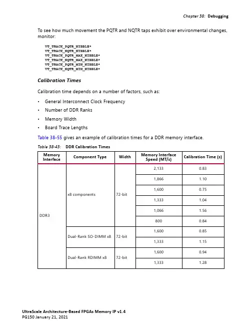
FPGA可编程逻辑器件芯片XC7K325T-2FFG900I中文规格书
- 格式:pdf
- 大小:517.33 KB
- 文档页数:5
Chapter1 Packaging OverviewAbout this GuideXilinx® 7series FPGAs include four FPGA families that are all designed for lowest power to enable a common design to scale across families for optimal power, performance, and cost.The Spartan®-7 family is the lowest density with the lowest cost entry point into the7series portfolio. The Artix®-7 family is optimized for highest performance-per-watt and bandwidth-per-watt for cost-sensitive, high-volume applications. The Kintex®-7 family is an innovative class of FPGAs optimized for the best price-performance. The Virtex®-7family is optimized for highest system performance and capacity.This 7series packaging and pinout product specification, part of an overall set ofdocumentation on the 7series FPGAs, is available on the Xilinx website .IntroductionThis section describes the pinouts for the 7series FPGAs in various fine pitch and flip-chip1.0mm pitch BGA packages, 0.8mm and 0.5mm pitch chip-scale packages, and 0.5mmpitch wire-bond lead frame packages.Spartan-7, Artix-7, and Kintex-7 devices are offered in low-cost, space-saving packages that are optimally designed for the maximum number of user I/Os.Virtex-7T and Virtex-7XT devices are offered exclusively in high performance flip-chip BGA packages that are optimally designed for improved signal integrity and jitter.For pinout and packaging information on the Virtex-7HT devices.Package inductance is minimized as a result of optimal placement and even distributionas well as an increased number of Power and GND pins.The FFG, FLG, FHG, FBG, SBG, and RFG flip-chip packages marked with the Pb-free Character on the upper right of the device are RoHS 6 of 6 compliant. The FFG, FLG, FHG, FBG, SBG, and RFG flip-chip packages not marked with the Pb-free character are RoHS 6 of 6 compliant,Pin DefinitionsTable1-12 lists the pin definitions used in 7series FPGAs packages.Note:There are dedicated general purpose user I/O pins listed separately in Table1-12. There are also multi-function pins where the pin names start with either IO_LXXY_ZZZ_# or IO_XX_ZZZ_#, where ZZZ represents one or more functions in addition to being general purpose user I/O. If not used for their special function, these pins can be user I/O.user I/O after stage 2 configuration is complete.Power/Ground PinsGND Dedicated N/A GroundRSVDGND Dedicated N/A Reserved pins, tie to GNDVCCAUX Dedicated N/A 1.8V power-supply pins for auxiliary circuits VCCAUX_IO_G#(2)Dedicated N/A 1.8V/2.0V power-supply pins for auxiliary I/O circuits VCCINT Dedicated N/A0.9V/1.0V power-supply pins for the internal core logic VCCO_#(3)Dedicated N/A Power-supply pins for the output drivers (per bank) VCCBRAM Dedicated N/A 1.0V power-supply pins for the FPGA logic block RAMVCCBATT_0Dedicated N/A Decryptor key memory backup supply; this pin should be tied to the appropriate V CC or GND when not used(4). Specific Spartan-7 devices (XC7S6 and XC7S15) do not support AES encryption. In these devices, connect VCCBATT_0 to VCCAUX or GND.VREF Multi-function N/A These are input threshold voltage pins. They become user I/Os when an external threshold voltage is not needed (per bank).Analog to Digital Converter (XADC) PinsFor more information, see the XADC Package Pins table in UG480, 7Series FPGAs and Zynq-7000 All Programmable SoC XADC Dual 12-Bit 1 MSPS Analog-to-Digital Converter User GuideVCCADC_0(5)(6)Dedicated N/A XADC analog positive supply voltageThe XC7S6 and XC7S15 Spartan-7 devices do not support the XADC. In these devices, connect the VCCADC_0 pin to VCCAUX.GNDADC_0(5)(6)Dedicated N/A XADC analog ground referenceThe XC7S6 and XC7S15 Spartan-7 devices do not support the XADC. In these devices, connect the GNDADC_0 pin to GND.VP_0(5)Dedicated Input XADC dedicated differential analog input (positive side) VN_0(5)Dedicated Input XADC dedicated differential analog input (negative side) VREFP_0(5)Dedicated N/A 1.25V reference inputVREFN_ 0(5)Dedicated N/A 1.25V reference GND referenceAD0P through AD15PAD0N through AD15N Multi-function Input XADC (analog-to-digital converter) differential auxiliary analog inputs 0–15.Auxiliary channels 6, 7, 13, 14, and 15 are not supported on Kintex-7 devices.Table 1-12:7Series FPGAs Pin Definitions (Cont’d)Pin Name Type Direction DescriptionChapter 2:7Series FPGAs Package Files。