7、Semiconductor-5
- 格式:ppt
- 大小:206.00 KB
- 文档页数:21

RTS5306EUSB 3.0 SD/MMC Card Reader ControllerDATASHEETDoc Rev. 1.012th October 2012TRADEMARKSRealtek is a trademark of Realtek Semiconductor Corporation. All other names mentioned in this document aretrademarks/registered trademarks of their respective owners.Realtek provides this document “as is”, without warranty of any kind, neither expressed nor implied, including, but not limited to the particular purpose. Realtek may make improvements and/or changes in this manual or in the product(s) and/or the program(s) described in this manual at any time. This document could include technical inaccuracies or typographical errors. Revision HistoryRevision Description Page Date1.00 Correct the package type for ordering information 9 2012/10/12 0.90 First release 2012/7/17Table of Contents1.G ENERAL D ESCRIPTION (1)2.F EA TURES (1)3.B LOCK D IAGRAM (3)4.P IN D ESCRIPTION (4)5.P IN A SSIGNMENT (5)6.E LECTRICAL C HARACTERISTICS (6)7.P ACKAGE D IMENSIONS (7)8.O RDERING I NFORMATION (9)1. General DescriptionThe Realtek RTS5306E USB3.0 Card Reader controller is based upon Universal Serial Bus 3.0 Specification, which integrates USB 3.0 and USB2.0 Transceivers, MCU, SIE, regulators and memory card access units into a single chip. It can be linked in Super Speed, High Speed or Full Speed operation and supports USB2.0/USB3.0 power saving mode. It provides 1LUN (Logic Unit Number) for Secure Digital TM and MultiMediaCard TM.The Realtek USB3.0 Card Reader supports both the internal MCU program ROM and external Serial Flash interface. With the external Serial flash interface, the control firmware could be easily re-configured through USB link. This could ease the software developing works and squeeze the prototyping schedule.The Realtek RTS5306E USB3.0 Card Reader integrates all regulators, clock generation circuitry and MOSFET components for switching card power, and could dramatically reduce the system BOM cost.2. FeaturesCompliant with Universal Serial Bus 3.0 Specification Revision 1.0Compliant with USB Mass Storage Class Bulk only Transport Specification Rev. 1.0Compliant with SD Part 1 Physical Layer Specification Version 3.01Compliant with MultiMediaCard System Specification version 4.4 with 4-bit data busSupport Super-Speed(5Gpbs), High-speed (480Mbps) and Full-speed (12Mbps) Data TransferUSB bus power operationSupport USB2.0 LPM / USB3.0 U1/U2/U3 power saving modeSupport Control, Bulk IN / OUT data pipesSupport the following memory card interfaces:-Secure Digital TM (SD), MultiMediaCard TM (MMC), Mini-SD, Micro-SD (T-flash), SDHC, SDXC,RS-MMC, Mobile-MMC, MMCPlus and MMC-microSupport SD card clock 208MHz (max.) for SDR104 mode.Support SD card clock 100MHz (max.) for SDR50 mode and 50MHz (max.) for DDR50 mode.Support SD Lock/Unlock FunctionSupport SD Jukebox application (CPRM function)Support hardware CRC (Cyclic Redundancy Check) functionProgrammable clock rate for flash memory card interfacesIntegrated Fast 8051 microprocessorExternal Serial Flash memory interfaceOn chip 3.3V and 1.2V regulatorsOn chip MOSFET components for direct power control of all types memory cards Support Spread Spectrum Clock for SD/MMC to reduce EMI effect32-pin QFN (5x5 mm) package for 1LUN solution3. Block Diagram4. Pin DescriptionPin# NameI/OTypeDescription1 SS_RX+ I USB3.0 SuperSpeed RX D+2 SS_RX- I USB3.0 SuperSpeed RX D-3 SS_TX+ O USB3.0 SuperSpeed TX D+4 SS_TX- O USB3.0 SuperSpeed TX D+5 USB3_A V12 Power Analog 1.2V for USB3.06 RREF I Connect an external resistor (6.2K ± 1%) to the Reference GND7 A V33 Power Analog 3.3V power8 VBUS I VBUS 5V power input9 XTLI I 12Mhz Crystal oscillator input10 XTLO O 12Mhz Crystal oscillator output11 USB2_A V12 Power Analog 1.2V power12 DM I/O USB2.0 D- signal13 DP I/O USB2.0 D+ signal14 VBUS I VBUS 5V power input15 D3V3 Power Digital 3.3V power16 CARD_3V3 O Power output to SD/MMC Card17 SDREG O Internal regulator for the SD card control signals. An external capacitor should be connected.18 SD_D1 I/O SD/MMC Card Data 119 SD_D0 I/O SD/MMC Card Data 020 SD_CLK O SD/MMC Card Clock Signal21 SD_CMD I/O SD/MMC Card Command Signal22 SD_D3 I/O SD/MMC Card Data 323 SD_D2 I/O SD/MMC Card Data 224 SD_WP I SD Card Write Protection pin25 DV12S Power Digital 1.2V power26 EEDO/MOSI I/O Serial Data Output to EEPROM or Serial Flash27 EESK/SCK I/O Clock Signal to EEPROM or Serial Flash28 EECS/CS# I/O Chip Select to EEPROM or Serial Flash29 EEDI/MISO I/O Serial Data Input from EEPROM or Serial Flash30 GPIO0 I/O General purpose input/output31 SD_CD# I SD/MMC Card Detection pin32 VDD_RX Power 1.2V Power for USB3.0 RX5. Pin AssignmentThe version number is shown in the location marked ‘VV’ and G means Green Package6. Electrical Characteristics6.1 Absolute Maximum RatingsSupply Voltage ……………………………………………………………………… –0.5V to +5.5V Operating Temperature Range ….………………………………………………….. 0°C to +70°CLatch up Current ……………………………………………………………………………… mA Electrostatic Discharge Voltage (HBM)………………………………………………………. KV6.2 DC CharacteristicsSymbol Description Conditions Min. Typ. Max. Unit V DD Supply Voltage 4.5 5 5.5 V V IH Input Voltage High 2.0 V V IL Input Voltage Low 0.8 V V OH Output Voltage High 3.0 V V OL Output Voltage Low 0.4 VC in Input Pin Capacitance 10 pFTBD mAI DD Supply Current 8051 is running @ 6MHz(Without memory card)I SUS Suspend Current D+ 1.5KΩ resistor is included TBD uA7. Package DimensionsPlastic Quad Flat No-Lead Package 32 Leads 5x5mm2 OutlineDimension in mm Dimension in inchSymbolMin Nom Max Min Nom MaxA 0.80 0.85 0.90 0.031 0.033 0.035 A1 0.00 0.02 0.05 0.000 0.001 0.002 A3 0.20 REF 0.008 REFA4 0.10 REF 0.004 REFb 0.18 0.25 0.30 0.007 0.010 0.012 D/E 5.00 BSC 0.020 BSCD2/E2 3.25 3.50 3.75 0.128 0.138 0.148e 0.50 BSC 0.020 BSCL 0.30 0.40 0.50 0.012 0.016 0.020Notes:1. CONTROLLING DIMENSION:MILLIMETER(mm).2. REFERENCE DOCUMENTL:JEDEC MO-220.8. Ordering InformationPart Number Package Status RTS5306E-GR QFN-32 Green package Available。

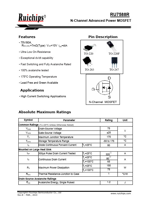
RU7088N-Channel Advanced Power MOSFETMOSFET Features Pin DescriptionApplicationsSymbol Parameter Rating Unit Common Ratings(T A=25°C Unless Otherwise Noted)V DSS Drain-Source Voltage70V GSS Gate-Source Voltage±25V T J Maximum Junction Temperature175°CT STG Storage Temperature Range-55 to 175°CI S Diode Continuous Forward Current T C=25°C80A Mounted on Large Heat SinkI DP300μs Pulse Drain Current Tested TC=25°C320AT C=25°C80①I D Continuous Drain CurrentT C=100°C60AT C=25°C150P D Maximum Power DissipationT C=100°C80W RθJC Thermal Resistance-Junction to Case 1.4°C/W Drain-Source Avalanche RatingsE AS Avalanche Energy, Single Pulsed150mJ •70V/80A,R DS (ON)=6.5mΩ (Type) V GS=10V I DS=40A•Ultra Low On-Resistance•Exceptional dv/dt capability•Fast Switching and Fully Avalanche Rated•100% avalanche tested•175°C Operating Temperature•Lead Free and Green Available•Switching Application Systems•Inverter SystemsAbsolute Maximum RatingsTO-220 TO-220FTO-263 TO-247N-Channel MOSFETElectrical Characteristics(T A =25°C Unless Otherwise Noted)RU7088SymbolParameter Test Condition Min.Typ.Max.UnitStatic Characteristics BV DSS Drain-Source Breakdown Voltage V GS =0V, I DS =-250µA 70V V DS = 70V, V GS =0V1I DSS Zero Gate Voltage Drain Current T J =85°C30µA V GS(th)Gate Threshold Voltage V DS =V GS , I DS =-250µA 234V I GSS Gate Leakage CurrentV GS =±25V, V DS =0V ±100nA R DS(ON)②Drain-Source On-state ResistanceV GS = 10V, I DS =40A6.59m ΩNotes:①Current limited by wire bond.②Pulse test ;Pulse width ≤300µs, duty cycle ≤2%.③Guaranteed by design, not subject to production testing.Diode Characteristics V SD②Diode Forward Voltage I SD =20A, V GS =0V 0.81 1.2V t rr Reverse Recovery Time 50ns Q rrReverse Recovery ChargeI SD =40A, dl SD /dt=100A/µs95nC Dynamic Characteristics③R G Gate ResistanceV GS =0V,V DS =0V,F=1MHz 1.4ΩC iss Input Capacitance 3100C oss Output Capacitance440C rss Reverse Transfer Capacitance V GS =0V,V DS = 30V,Frequency=1.0MHz260pFt d(ON)Turn-on Delay Time 1832t r Turn-on Rise Time 1528t d(OFF)Turn-off Delay Time 63110t fTurn-off Fall TimeV DD =30V, R L =30Ω,I DS =1A, V GEN =10V,R G =8Ω3360nsGate Charge Characteristics③Q g Total Gate Charge 75108Q gs Gate-Source Charge 14Q gdGate-Drain ChargeV DS =30V, V GS =10V,I DS =40A25nCTypical CharacteristicsPower DissipationDrain CurrentP t o t -P o w e r (W )I D - D r a i n C u r r e n t (A )T j - Junction Temperature (°C)T j - Junction Temperature (°C)Safe Operation AreaThermal Transient ImpedanceI D - D r a i n C u r r e n t (A )N o r m a l i z e d E f f e c t i v e T r a n s i e n tV DS - Drain-Source Voltage (V)Square Wave Pulse Duration (sec)Typical CharacteristicsOutput CharacteristicsDrain-Source On ResistanceI D - D r a i n C u r r e n t (A )R D S (O N )- O n R e s i s t a n c e (m Ω)V DS - Drain-Source Voltage (V)I D -Drain Current (A)Drain-Source On Resistance Gate Threshold VoltageR D S (O N )- O n - R e s i s t a n c e (m )N o r m a l i z e d T h r e s h o l d V o l t a g eV GS -Gate-Source Voltage (V)T j - Junction Temperature (°C)Typical CharacteristicsDrain-Source On ResistanceSource-Drain Diode ForwardN o r m a l i z e d O n R e s i s t a n c eI S - S o u r c e C u r r e n t (A )T j - Junction Temperature (°C)V SD - Source-Drain Voltage (V)CapacitanceGate ChargeC - C a p a c i t a n c e (p F )V G S - G a t e -S o u r c e V o l t a g e (V )V DS - Drain-Source Voltage (V)Q G - Gate Charge (nC)Avalanche Test Circuit and WaveformsSwitching Time Test Circuit and WaveformsOrdering and Marking InformationRU7088Package (Available)R : TO-220; S: TO-263 ; P: TO-220FOperating Temperature RangeC :-55 to 175 ºCAssembly MaterialG : Green & Lead FreePackagingT : TUBETR : Tape & ReelPackage InformationTO-220FB-3LALL DIMENSIONS REFER TO JEDEC STANDARD DO NOT INCLUDE MOLD FLASH OR PROTRUSIONSMMINCH MMINCH SYMBOLMIN NOM MAX MIN NOM MAX SYMBOL MIN NOM MAX MIN NOM MAX A 4.40 4.57 4.700.1730.1800.185Øp1 1.401.50 1.600.0550.0590.063A1 1.27 1.30 1.330.0500.0510.052e 2.54BSC 0.1BSC A2 2.35 2.40 2.500.0930.0940.098e1 5.08BSC 0.2BSC b 0.77-0.900.030-0.035H1 6.40 6.50 6.600.2520.2560.260b2 1.23- 1.360.048-0.054L 12.75-13.170.502-0.519C 0.480.500.520.0190.0200.021L1-- 3.95--0.156D 15.4015.6015.800.6060.6140.622L2 2.50REF.0.098REF.D19.009.109.200.3540.3580.362Øp 3.57 3.60 3.630.1410.1420.143DEP 0.050.100.200.0020.0040.008Q2.73 2.80 2.870.1070.1100.113E 9.709.9010.100.3820.3890.398θ15°7°9°5°7°9°E1-8.70--0.343-θ21°3°5°1°3°5°E29.8010.0010.200.3860.3940.401TO-263-2LALL DIMENSIONS REFER TO JEDEC STANDARD DO NOT INCLUDE MOLD FLASH OR PROTRUSIONSMMINCH MMINCH SYMBOLMIN NOM MAX MIN NOM MAX SYMBOLMIN NOM MAX MIN NOM MAX A 4.40 4.57 4.700.1730.1800.185L 2.00 2.30 2.600.0790.0900.102A100.100.2500.0040.010L3 1.17 1.27 1.400.0460.0500.055A2 2.59 2.69 2.790.1020.1060.110L1-- 1.70--0.067b 0.77-0.900.030-0.035L40.25BSC 0.01BSC b1 1.23- 1.360.048-0.052L22.50REF.0.098REF.c 0.34-0.470.013-0.019θ0°-8°0°-8°C1 1.22- 1.320.048-0.052θ15°7°9°5°7°9°D 8.608.708.800.3380.3430.346θ21°3°5°1°3°5°E 10.0010.1610.260.3940.40.404DEP 0.050.100.200.0020.0040.008e 2.54BSC 0.1BSC Øp11.401.501.600.0550.0590.063H14.7015.1015.500.5790.5940.610TO-220F-3LALL DIMENSIONS REFER TO JEDEC STANDARD DO NOT INCLUDE MOLD FLASH OR PROTRUSIONSMMINCH MMINCH SYMBOLMIN NOM MAX MIN NOM MAX SYMBOL MIN NOM MAX MIN NOM MAX E 9.9610.1610.360.3920.4000.408Øp3- 3.450--0.136-A 4.50 4.70 4.900.1770.1850.193θ15°7°9°5°7°9°A1 2.34 2.54 2.740.0920.1000.108θ2-45°--45°-A20.95 1.05 1.150.0370.0410.045DEP 0.050.100.150.0020.0040.006A30.420.520.620.0170.0200.024F1 1.90 2.00 2.100.0750.0790.083A4 2.65 2.75 2.850.1040.1080.112F213.6113.8114.010.5360.5440.552c -0.50--0.020-F3 3.20 3.30 3.400.1260.1300.134D 15.6715.8716.070.6170.6250.633G 3.25 3.45 3.650.1280.1360.144Q 8.809.009.200.3460.3540.362G1 5.90 6.00 6.100.2320.2360.240H1 6.48 6.68 6.880.2550.2630.271G2 6.907.007.100.2720.2760.280e 2.54BSC 0.1BSC b1 1.17 1.20 1.240.0460.0470.048Øp - 3.183--0.125-b20.770.80.850.0300.0310.033L 12.7812.9813.180.5030.5110.519b3 1.10 1.30 1.500.0430.0510.059D18.999.199.390.3540.3620.370E19.810.0010.200.3860.3940.412Øp1 1.40 1.50 1.600.0550.0590.063K10.750.80.850.0300.0310.033Øp21.151.201.250.0450.0470.049Copyright© Ruichips Semiconductor Co., Ltd Rev.B– JUN.,RU7088Customer ServiceWorldwide Sales and Service:Sales@Technical Support:Technical@Investor Relations Contacts:Investor@Marcom Contact:Marcom@Editorial Contact:Editorial@HR Contact:HR@Legal Contact:Legal@Shen Zhen RUICHIPS Semiconductor CO., LTDRoom501,the5floor An Tong Industrial Building,NO.207Mei Hua Road Fu Tian Area Shen Zhen City,CHINA TEL:(86-755) 8311-5334FAX: (86-755) 8311-4278E-mail: Sales-SZ@。


单词频率释义national 27国家的according 23依照alert 23警报university 22大学product 22产品battery 18电池device 18装置,设备receive 17接受,接收increase 17增加campus 17校园award 16奖品service 15服务information 14信息project 14计划,方案financial 14财政的,金融的crime 13犯罪program 13节目,程序package 13包裹robot 12机器人step 12脚步,步伐education 12教育federal 12联邦的tax 12税recycle 11再循环,回收online 11在线store 11储存,储藏nuclear 11核author 10作者provide 10提供article 10文章quality 10品质,质量website 10网站festival 10节日medical 10药的,内科的state 10情形,国家concern 10涉及,关系到wheelchair 10轮椅museum 9博物馆report 9报告future 9未来,将来economic 9经济design 9设计government 9政府material 9材料power 8力量organization 8组织energy 8能量disaster 8灾难emergency 8紧急情况present 8目前,礼物professor 8教授industry 8工业subject 8主题;科目effort 8成就;努力cause 8原理research 7研究poet 7诗人include 7包括safety 7安全性semiconductor 7半导体member 7成员tobacco 7烟草amount 7总数diagnose 7诊断reduce 7减少describe 7描述infer 7推理,推断prize 6奖品signal 6信号damage 6破坏environment 6环境technology 6技术exhibition 6展览improve 6提高encourage 6鼓励academy 6学会;学院consumer 6消费者management 6管理marketplace 6市场community 6社区brain 6大脑underline 6在……下面划线smoke 6烟teenager 6十几岁的青少年involve 6包括,笼罩immigrant 6移来的,移民的legacy 6遗产lack 6缺乏adult 6成年人publish 6出版,刊印action 6动作、行动however 5但是decade 5十年、十teen 5青少年below 5在……下面title 5头衔entitleexpect 5期待laboratory 5实验室special 5特别的effective 5有效的millisecond 5毫秒charge 5费用、充电hurricane 5飓风administrator 5管理人partner 5合伙人scalp 5头皮cap 5帽子deal 5交易loan 5贷款、借出media 5媒体natural 5自然的necessary 5必须的benefit 5利益,好处effect 5结果,效果develop 5发展salesman 5售货员produce 5制造offer 5提供,出价excite 5刺激,使兴奋solution 5解答,解决办法poetry 5诗,诗意merchant 5商人application 5请求,申请,应用drug 5药,毒品recent 5最近的form 5形状,外形wireless 5无线的complete 5全部的,完全的major 5主修课fuss 4大惊小怪career 4职业electrical 4电的rent 4租debt 4债务square 4正方形,广场unite 4联合,团结attack 4攻击,袭击promote 4促进,提升,distributor 4发行人variety 4变化,多样性command 4命令,掌握disable 4使残废source 4来源protect 4保护solid 4固体,立体afford 4供得起shock 4振动,震惊tuition 4学费force 4力量,武力statistic 4统计数据environmental 4环境的raise 4上升,提出purpose 4目的,意图possible 4可能的success 4成功expert 4专家brochure 4小册子issue 4出版,发行social 4社会的mention 4说起,提起attitude 4姿势,态度global 4全球的apply 4申请,适用manage 4处理break 4休息,暂停volunteer 4志愿者case 4案例overweight 4超重generation 4产生,一代人cozy 4舒适的latest 4最近的magazine 4杂志sensor 4传感器reasonable 4合理的operate 4操作,运转profit 4利润,益处journey 4旅行toward 4向,对于literature 4文学ski 4雪橇滑雪interview 4接见,会见handle 4手柄,处理respond 4回答,响应wristband 3袖口prevent 3防止,预防similar 3相似的comparison 3比较,对照director 3主任,导演collection 3收藏,收集require 3需要,要求carrier 3运送者approve 3赞成,同意deliver 3递送,传递inspire 3鼓舞,启发creative 3创造性的creativity 3创造力organize 3组织motivate 3激发advantage 3优势matter 3时间,问题regular 3有规律的retire 3退休choice 3选择illness 3疾病especially 3尤其是discuss 3讨论insurance 3保险order 3次序lazy 3懒的measure 3尺寸,测量increasingly 3日益增加地weight 3重量attract 3吸引deadly 3致命的attach 3系上,附上survey 3调查opinion 3意见patient 3病人,耐心的pressure 3压力scientist 3科学家average 3平均rate 3比率crisis 3危机crowd 3人群relate 3使联系colleague 3同事press 3按,压;媒体degree 3程度,学位legal 3合法的remove 3移除appear 3出现liquid 3液体item 3项目,条款intend 3打算fund 3资金;投资continue 3继续sign 3标志collect 3收集charity 3慈善cure 3治愈dismiss 3解散,解雇greenhouse 3温室burn 3燃烧critic 3批评,批评家arctic 3北极的expedition 3远征,探险suffer 3遭受customer 3消费者establish 3建立wildlife 3野生动植物novelist 3小说家prove 3证明request 3要求master 3主人,雇主slavery 3奴隶supplier 3供应者personal 3个人的outstanding 3杰出的repair 3修理join 3加入delight 3高兴,快乐department 3部门,系proof 3证据effectiveness 3有效性promoter 3促销者resource 3资源movement 3运动,动作progress 3进步truth 3事实、真理victim 3受害人,牺牲品camera 3相机classic 3杰作,名著international 3国际的protection 2保护positive 2积极的proposal 2提议,建议access 2道路,访问robotic 2机器人的experiment 2实验read 2读distribute 2分发,分配kindness 2仁慈,亲切explain 2解释litter 2垃圾yard 2院子couple 2一对,夫妇unexpected 2意料之外的spinal 2脊骨的touch 2接触dozen 2一打watchdog 2看门狗security 2安全(完整版)高考英语阅读理解历年真题高频词汇routinely 2例行公事地express 2表达cafeteria 2自助餐厅smoothly 2平稳的multicultural 2多元文化的vehicle 2交通工具,车辆communication 2交流improvement 2提升network 2网络particularly 2独特的,显著former 2以前的estimate 2估计trend 2潮流participation 2分享,参与furniture 2家具photographer 2摄影师accurate 2精确的ability 2能力mobile 2移动的timely 2及时的volume 2卷,音量wish 2希望splendid 2壮丽的strength 2力量infrastructure 2基础设施restaurant 2饭店administration 2管理chain 2链条,连锁campaign 2战役prizewinner 2得奖人human 2人类read 2读satisfy 2满意billboard 2布告板donate 2捐赠kick 2踢doubt 2怀疑tolerance 2宽容,容忍storefront 2店面error 2错误remind 2提醒trial 2实验unconcern 2不关心sympathy 2同情figure 2外形,轮廓,图形sector 2区域intrigue 2激起兴趣trust 2信任native 2本地人uncertainty 2不确定性note 2笔记arise 2出现wise 2明智sense 2感觉print 2印刷disease 2疾病schedule 2时间表circle 2圆圈playmate 2玩伴operator 2操作员draw 2画,吸引attention 2注意力unnecessary 2不必要的garage 2车库,汽车修理厂notice 2注意associate 2使联合communicate 2交流recently 2最近over-consumption 2过度消费household 2家庭。
MFG 常用英文单字Semiconductor半导体导体、绝缘体和半导体主要依据导电系数的大小,决定了电子的移动速度。
导体:金、银、铜、铁、人、水……导电系数大,传导绝缘体:塑料、木头、皮革、纸……导电系数小、传导不半导体:硅中加锗、砷、镓、磷……平时不导电加特定电压后导电Wafer 芯片或晶圆:原意为法国的松饼,饼干上有格子状的饰纹,与FAB内生产的芯片图形类Lot 批;一批芯片中最多可以有25片,最少可以只有一片。
ID Identification的缩写。
用以辨识各个独立的个体,就像公司内每一个人有自己的识别证。
Wafer ID 每一片芯片有自己的芯片刻号,叫Wafer ID。
Lot ID 每一批芯片有自己的批号,叫Lot ID。
Part ID 各个独立的批号可以共享一个型号,叫Part ID。
WIP Work In Process,在制品。
从芯片投入到芯片产品,FAB内各站积存了相当数量的芯片,统称为FAB内的WIP 。
一整个制程又可细分为数百个Stage和Step,每一个Stage所堆积的芯片,称为Stage WIP。
Lot Priority 每一批产品在加工的过程中在WIP中被选择进机台的优先级。
Super Hot Run的优先级为1,视为等级最高,必要时,当Lo上一站加工时,本站便要空着机台等待Super Hot RuHot Run的优先级为2,紧急程度比Super Hot Run次一级。
Normal的优先级为3,视为正常的等级,按正常的派货原则视常班向生产指令而Cycle time 生产周期,FAB Cycle Time 定义为:从芯片投入到芯片产生的这一段时间。
Stage Cycle Time:Lot从进站等候开始到当站加工后出货时间点截Spec. 规格Specification的缩写。
产品在机台加工过程中,每一站均设定规格。
机台加工后,产品或控片经由量测机台量测,该产品加工后,是否在规格内。
February 5, 2008 LM2500742V, 0.5A Step-Down Switching RegulatorGeneral DescriptionThe LM25007 is a monolithic step-down switching regulator featuring all of the functions needed to implement a low cost, efficient, power supply. Capable of driving a 0.5Amp load over a 9V-42V input voltage range, this device is easy to apply and is provided in the small MSOP-8 and the thermally enhanced LLP-8 packages. Ultra-fast transient response is achieved through the use of a constant on-time architecture with Vin feed forward. This feature provides an almost constant oper-ating frequency over load and input voltage variations. The operating frequency can be adjusted with a single resistor. This architecture is easy to use and tolerant of component selection. An intelligent current limit is implemented in the LM25007 with forced off time that is inversely proportional to Vout thus ensuring recovery from fault conditions. The output voltage may be set from 2.5V to >30V. To improve efficiency in light load applications, the Vcc pin can be connected to an external voltage source to eliminate the drop through the in-ternal regulator. Additional features include: thermal shut-down, Vcc under-voltage lockout, gate drive under-voltage lockout, and max duty cycle limiter.Features■Integrated 0.74 ohm N-Channel MOSFET switch■Guaranteed 0.5Amp output current■Ultra-Fast Transient Response■Up to 800kHz operation■No control loop compensation required■Vin feed forward provides constant operating frequency ■2% accurate 2.5V feedback from -40°C to 125°C■Highly efficient operation■Intelligent current limit protection■External shutdown control■Thermal shutdown■MSOP-8 and thermally enhanced LLP packages Typical Applications■12VDC and 24VDC distributed rail systems■24VAC systems■Automotive body electronics and telematics■Industrial systems■HB-LED constant current sourcePackage■MSOP - 8■LLP - 8 (4mm x 4mm)Basic Step-Down Regulator20165513© 2008 National Semiconductor LM25007 42V, 0.5A Step-Down Switching RegulatorConnection Diagram201655028-Lead MSOP, LLPOrdering InformationOrder Number Package Type NSC Package DrawingSupplied AsLM25007MM MSOP-8MUA08A 1000 Units on Tape and Reel LM25007MMX MSOP-8MUA08A 3500 Units on Tape and Reel LM25007SD LLP-8SDC08A 1000 Units on Tape and Reel LM25007SDXLLP-8SDC08A4500 Units on Tape and ReelPin DescriptionsPin Name DescriptionApplication Information1SW Switching NodePower switching node. Connect to the inductor,bootstrap capacitor, and free-wheeling diode.2BSTBoost Boot–strap capacitor inputAn external capacitor is required between the BST and the SW pins. A 0.01µF ceramic capacitor is recommended.3RCL Current Limit OFF time programming pinA resistor between this pin and RTN sets the off-time when current limit is detected. The off-time is preset to 17 µs if FB = 0V .4RTN Circuit Ground5FBFeedback Signal from Regulated OutputThis pin is connected to the inverting input of the internal regulation comparator. The regulation threshold is 2.5V.6RON/SD On-time set pinA resistor between this pin and VIN sets the switch on-time as a function of Vin. The minimum recommended on-time is 300ns at the maximum input voltage.7VCCOutput from the internal high voltage bias regulator.If an auxiliary voltage is available to raise the voltageon this pin above the regulation setpoint (7V), the internal series pass regulator will shutdown, reducing the IC power dissipation. Do not exceed 14V. This output provides gate drive power for the internal Buck switch. An internal diode is provided between this pin and the BST pin. A local 0.1uF decoupling capacitor is recommended.8VIN Input supply voltageRecommended operating range: 9V to 42V.-EPExposed pad, underside of the LLP package option Exposed metal pad on the LLP package underside. Itis recommended to connect this pad to the PC board ground plane to aid in heat dissipation. 2L M 25007Typical Application Circuit and Block Diagram20165501 LM25007Absolute Maximum Ratings (Note 1)If Military/Aerospace specified devices are required,please contact the National Semiconductor Sales Office/Distributors for availability and specifications.VIN to RTN 45V BST to RTN59V SW to RTN (Steady State)-1V ESD Rating (Note 5) Human Body Model2kVBST to V CC 45V BST to SW 14V VCC to RTN14VAll Other Inputs to RTN-0.3 to 7VStorage Temperature Range -65°C to +150°COperating Ratings(Note 1)V IN9V to 42VJunction Temperature−40°C to + 125°CElectrical CharacteristicsSpecifications with standard type are for T J = 25°C only; limits in boldface type apply over the full Operating Junction Temperature (T J ) range. Minimum and Maximum limits are guaranteed through test, design, or statistical correlation. Typical values represent the most likely parametric norm at T J = 25°C, and are provided for reference purposes only. Unless otherwise stated the following conditions apply: V IN = 24V, R ON = 200k Ω. (Note 3).Symbol ParameterConditionsMinTypMaxUnitsStartup Regulator V CC Reg V CC Regulator Output 6.677.4VV CC Current Limit(Note 4)11mAV CC Supply V CC undervoltage Lockout Voltage (V CC increasing) 6.3 V V CC Undervoltage Hysteresis206 mV V CC UVLO Delay (filter) 3 µs Operating Current (I CC )Non-Switching, FB = 3V 500675µA Shutdown/Standby Current RON/SD = 0V 70150µA Switch CharacteristicsBuck Switch Rds(on)I TEST = 200mA,VBST −VSW = 6.3V (Note 6)0.741.34ΩGate Drive UVLO (VBST – VSW)Rising 3.4 4.5 5.5VGate Drive UVLO Hysteresis 400 mV Current Limit Current Limit Threshold535725900mA Current Limit Response Time I switch Overdrive = 0.1A Time to Switch Off 225 ns OFF time generator (test 1)FB=0V, RCL = 100K 17 µs OFF time generator (test 2)FB=2.3V, RCL = 100K 2.65 µs On Time GeneratorTON -1Vin = 10V Ron = 200K 2.15 2.77 3.5µs TON -2Vin = 40V Ron = 200K 450615810ns Remote Shutdown Threshold Rising 0.450.7 1.1VRemote Shutdown Hysteresis40mV 4L M 25007Symbol Parameter Conditions Min Typ Max Units Minimum Off TimeMinimum Off Timer FB = 0V300ns Regulation and OV ComparatorsFB Reference Threshold Internal referenceTrip point for switch ON2.445 2.5 2.550VFB Over-Voltage Threshold Trip point for switch OFF 2.875VFB Bias Current100nA Thermal ShutdownTsd Thermal Shutdown Temp.165°C Thermal Shutdown Hysteresis25°C Thermal ResistanceθJA Junction to Ambient MUA Package200°C/WSDC Package40°C/WNote 1:Absolute Maximum Ratings are limits beyond which damage to the device may occur. Operating Ratings are conditions under which operation of the device is intended to be functional. For guaranteed specifications and test conditions, see the Electrical Characteristics.Note 2:For detailed information on soldering plastic MSOP and LLP packages, refer to the Packaging Data Book available from National Semiconductor Corporation.Note 3:All limits are guaranteed. All electrical characteristics having room temperature limits are tested during production with TA = TJ= 25°C. All hot and coldlimits are guaranteed by correlating the electrical characteristics to process and temperature variations and applying statistical process control.Note 4:The VCCoutput is intended as a self bias for the internal gate drive power and control circuits. Device thermal limitations limit external loading.Note 5:The human body model is a 100pF capacitor discharge through a 1.5kΩ resistor into each pin. The human body ESD compliance level for Pin 7 and 8is 1000V.Note 6:For devices procurred in the LLP-8 package the Rds(on) limits are guaranteed by design characterization data only.LM25007Typical Performance CharacteristicsOperational Waveforms20165508LM25007 Operation: VOUT= 10V, VIN= 20V, IOUT= 250mACH1: Switch Node, CH2: VOUT(AC), CH4: Inductor CurrentOperational Waveforms20165509LM25007 Operation: VOUT= 10V, VIN= 42V, IOUT= 250mACH1: Switch Node, CH2: VOUT(AC), CH4: Inductor CurrentLM25007 10V Output Efficiency20165510Current Limit Off-Time vs VFB20165511VINvs TONRON= 100k, 200k, 300k201655126LM257Detailed Operating DescriptionThe LM25007 is a monolithic step-down switching regulator featuring all of the functions needed to implement low cost,efficient, power supply. Capable of driving a 0.5Amp load over a 9-42V input voltage range, this device is easy to apply and is provided in the small MSOP-8 and the thermally enhanced LLP-8 packages. Ultra-fast transient response is achieved through the use of a constant on-time architecture with Vin feed forward. This feature provides and almost constant op-erating frequency over load and input voltage variations. The operating frequency may be adjusted up to 800kHz depend-ing on input and output voltages. This architecture is easy to use and tolerant of component selection. An intelligent current limit is implemented in the LM25007 with forced off time that is inversely proportional to Vout to ensure recovery from fault conditions. The output voltage may be set from 2.5V to >30V.To improve efficiency in light load applications, the Vcc pin can be tied to an external voltage source thus eliminating the drop through the integrated internal regulator. Additional pro-tection features include: thermal shutdown, Vcc under-volt-age lockout, gate drive under-voltage lockout, and max duty cycle limiter.Hysteretic Control Circuit OverviewThe LM25007 is a Buck DC-DC regulator that uses a constant on-time control scheme. The on-time is programmed by an external resistor and varies inversely with line input voltage (Vin). The core regulation elements of the LM25007 are the feedback comparator and the on-time one-shot. The regulator output voltage is sensed at the feedback pin (FB) and is com-pared to an internal reference voltage (2.5V). If the FB signal is below the reference voltage, the buck switch is turned on for a fixed time pulse determined by the line voltage and a programming resistor (R ON ). Following the on period the switch will remain off for at least the minimum off timer period of 300ns. If the FB pin voltage is still below the reference after the 300ns off-time, the switch will turn on again for another on time period. This switching behavior will continue until the FB pin voltage reaches the reference voltage level.The LM25007 operates in discontinuous conduction mode at light load currents or continuous conduction mode at heavier load currents. In discontinuous conduction mode, current through the output inductor starts at zero and ramps up to a peak value during the buck switch on-time and then back to zero during the off-time. The inductor current remains at zero until the next on-time period starts when FB falls below the internal reference. In discontinuous mode the operating fre-quency is relatively low and will vary with load. Therefore at light loads the conversion efficiency is maintained, since the switching losses decrease with the reduction in load current and switching frequency. The approximate discontinuous mode operating frequency can be calculated as follows:In continuous conduction mode, current flows continuously through the inductor and never ramps down to zero. In this mode the operating frequency is greater than the discontinu-ous mode frequency and remains relatively constant with load and line variations. The approximate continuous mode oper-ating frequency can be calculated as follows:The output voltage (Vout) can be programmed by two external resistors as shown in Figure 1. The regulated voltage is cal-culated as follows:V OUT = 2.5 x (R3 + R4) / R4The feedback comparator in hysteretic regulators depends on the output ripple voltage to switch the output transistor on and off at regular intervals. In order for the internal comparator to respond quickly to changes in output voltage, proportional to inductor current, a minimum amount of capacitor Equivalent Series Resistance (ESR) is required. A ripple voltage of 25mV is recommended at the feedback pin (FB) for stable operation.In cases where the intrinsic capacitor ESR is too small, addi-tional series resistance may be added.For applications where lower output voltage ripple is required the load can be connected directly to the low ESR output ca-pacitor, as shown in Figure 1. The series resistor (R5) will degrade the load regulation. Another technique for enhancing the ripple voltage at the FB pin is to place a capacitor in par-allel with the feedback divider resistor R3. The addition of the capacitor reduces the attenuation of the ripple voltage from the feedback divider.High Voltage Bias Regulator (VCC)The LM25007 contains an internal high voltage bias regulator.The input pin (Vin) can be connected directly to line voltages from 9 to 42 Volts. To avoid supply voltage transients due to long lead inductances on the input pin (VIN), it is always rec-ommended to connect a low ESR ceramic chip capacitor (≊0.1µF) between VIN and RTN pins located close to the LM25007. The regulator is internally current limited to 11mA.Upon power up, the regulator is enabled and sources current into an external capacitor connected to the VCC pin. When the voltage on the VCC pin reaches its UVLO level (6.3V), the controller output is enabled.An external auxiliary supply voltage can be diode connected to the Vcc pin. If the auxiliary voltage is greater than 7 Volts the internal regulator will shutoff, thus reducing internal power dissipation. Do not exceed 14V at VCC. See Figure 2.LM2500720165505FIGURE 1. Low Ripple Output Configuration20165506FIGURE 2. Self Biased Configuration 8L M 25007Over-Voltage ComparatorThe over-voltage comparator is provided to protect the output from overvoltage conditions due to sudden input line voltage changes or output loading changes. The over-voltage com-parator monitors the FB pin versus an internal 2.875V refer-ence. If the voltage at FB rises above 2.875V the comparator immediately terminates the buck switch on-time pulse.ON Time generator and ShutdownThe on-time of the LM25007 is set inversely proportional to the input voltage by an external resistor connected between RON/SD and VIN. The RON/SD terminal is a low impedance input biased at approximately 1.5V. The current through the resistor and into the RON/SD pin is approximately propor-tional to Vin and used internally to control the on-timer. This scheme of input voltage feed-forward hysteretic operation achieves nearly constant operational frequency over varying line and load conditions. The on-time equation for the LM25007 is :Ton = 1.42 x 10⁻¹⁰ x R ON / V INThe RON/SD pin of the LM25007 also provides a shutdown function which disables the regulator and significantly de-creases quiescent power dissipation. By pulling the pin below 0.7V activates the low power shutdown mode. The V IN qui-escent current in the shutdown mode is approximately 100µA internal to the LM25007 plus the current in the R ON resistor.See Figure 320165507FIGURE 3. Shutdown ImplementationCurrent LimitThe LM25007 contains an intelligent current limit off-timer in-tended to reduce the foldback characteristic inherent with fixed off-time over-current protection. If the current in the Buck switch exceeds 725mA the present cycle on-time is immedi-ately terminated (cycle by cycle current limit). Following the termination of the cycle a non-resetable current limit off timer is initiated. The duration of the off time is a function of the external resistor (RCL) and the FB pin voltage. When the FB pin voltage equals zero, the current limit off-time is internally preset to 17µs. This condition occurs in short circuit operation when a maximum amount of off-time is required.In cases of overload (not complete short circuit) the current limit off-time is reduced as a function of the output voltage (measured at the FB pin). Reducing the off-time with smaller overloads reduces the amount of foldback and also reduces the initial start-up time. The current limit off time for a given FB pin voltage and R CL resistor can be calculated by the fol-lowing equation:Toff = 10-5 / (0.59 + (V FB / 7.22 x 10⁻⁶ x R CL ))Applications utilizing low resistance inductors and/or a low voltage drop rectifier may require special evaluation at high line, short circuit conditions. In this special case the preset17µs (FB = 0V) off-time may be insufficient to balance the inductor volt*time product. Additional inductor resistance, out-put resistance or a larger voltage drop rectifier may be nec-essary to balance the inductor cycle volt*time product and limit the short circuit current.N - Channel Buck Switch and DriverThe LM25007 integrates an N-Channel Buck switch and as-sociated floating high voltage gate driver. The gate driver circuit works in conjunction with an external bootstrap capac-itor and an internal high voltage diode. The bootstrap capac-itor is charged by V CC through the internal high voltage diode.A 0.01uF ceramic capacitor connected between the BST pin and SW pin is recommended.During each cycle when the Buck switch turns off, the SW pin is approximately 0V. When the SW pin voltage is low, the bootstrap capacitor is charged from Vcc through the internal diode. The minimum off timer, set to 300ns, ensures that there will be a minimum interval every cycle to recharge the boot-strap capacitor.An external re-circulating diode from the SW pin to ground is necessary to carry the inductor current after the internal Buck switch turns off. This external diode must be of the Ultra-fast or Schottky type to reduce turn-on losses and current over-LM25007shoot. The reverse voltage rating of the re-circulating diode must be greater than the maximum line input voltage.Thermal ProtectionInternal Thermal Shutdown circuitry is provided to protect the integrated circuit in the event the maximum junction temper-ature is exceeded. When thermal protection is activated,typically at 165 degrees Celsius, the controller is forced into a low power reset state, disabling the output driver. This fea-ture is provided to prevent catastrophic failures from acciden-tal device overheating.Minimum Load CurrentA minimum load current of 1 mA is required to maintain proper operation. If the load current falls below that level, the boot-strap capacitor may discharge during the long off-time, and the circuit will either shutdown, or cycle on and off at a low frequency. If the load current is expected to drop below 1 mA in the application, the feedback resistors should be chosen low enough in value so they provide the minimum required current at nominal Vout.10V, 400mA Demo Board Bill of Materials (See Typical Application Circuit)ITEM PART NUMBER DESCRIPTION VALUE C1C4532X7R2A105M CAPACITOR, CER, TDK 1µ, 100V C2C4532X7R1E156M CAPACITOR, CER, TDK 15µ, 25V C3C1206C104K5RAC CAPACITOR, CER, KEMET 0.1µ, 50V C4C1206C103K5RAC CAPACITOR, CER, KEMET 0.01µ, 50V C5C3216X7R2A104KTCAPACITOR, CER, TDK 0.1µ, 100VD1MURA110T3DIODE, 100V, ON SEMI L1SLF7045T-101MR60-1BUCK INDUCTOR, TDK100µH R1CRCW12062003F RESISTOR 200K R2CRCW12061003F RESISTOR 100K R3CRCW12063011F RESISTOR 3.01K R4CRCW12061001F RESISTOR 1K R5CRCW12061R00FRESISTOR1U1LM25007REGULATOR, NATIONAL 10L M 25007Physical Dimensions inches (millimeters) unless otherwise noted8-Lead MSOP PackageNS Package Number MUA08A8-Lead LLP PackageNS Package Number SDC08A LM25007L M 25007 42V , 0.5A S t e p -D o w n S w i t c h i n g R e g u l a t o rFor more National Semiconductor product information and proven design tools, visit the following Web sites at:ProductsDesign SupportAmplifiers /amplifiers WEBENCH /webench Audio/audio Analog University /AU Clock Conditioners /timing App Notes /appnotes Data Converters /adc Distributors /contacts Displays /displays Green Compliance /quality/green Ethernet /ethernet Packaging/packaging Interface /interface Quality and Reliability /quality LVDS/lvds Reference Designs /refdesigns Power Management /power Feedback /feedback Switching Regulators /switchers LDOs /ldo LED Lighting /led PowerWise/powerwise Serial Digital Interface (SDI)/sdiTemperature Sensors /tempsensors Wireless (PLL/VCO)/wirelessTHE CONTENTS OF THIS DOCUMENT ARE PROVIDED IN CONNECTION WITH NATIONAL SEMICONDUCTOR CORPORATION (“NATIONAL”) PRODUCTS. NATIONAL MAKES NO REPRESENTATIONS OR WARRANTIES WITH RESPECT TO THE ACCURACY OR COMPLETENESS OF THE CONTENTS OF THIS PUBLICATION AND RESERVES THE RIG HT TO MAKE CHANG ES TO SPECIFICATIONS AND PRODUCT DESCRIPTIONS AT ANY TIME WITHOUT NOTICE. NO LICENSE, WHETHER EXPRESS,IMPLIED, ARISING BY ESTOPPEL OR OTHERWISE, TO ANY INTELLECTUAL PROPERTY RIG HTS IS G RANTED BY THIS DOCUMENT.TESTING AND OTHER QUALITY CONTROLS ARE USED TO THE EXTENT NATIONAL DEEMS NECESSARY TO SUPPORT NATIONAL’S PRODUCT WARRANTY. EXCEPT WHERE MANDATED BY G OVERNMENT REQUIREMENTS, TESTING OF ALL PARAMETERS OF EACH PRODUCT IS NOT NECESSARILY PERFORMED. NATIONAL ASSUMES NO LIABILITY FOR APPLICATIONS ASSISTANCE OR BUYER PRODUCT DESIG N. BUYERS ARE RESPONSIBLE FOR THEIR PRODUCTS AND APPLICATIONS USING NATIONAL COMPONENTS. PRIOR TO USING OR DISTRIBUTING ANY PRODUCTS THAT INCLUDE NATIONAL COMPONENTS, BUYERS SHOULD PROVIDE ADEQUATE DESIGN, TESTING AND OPERATING SAFEGUARDS.EXCEPT AS PROVIDED IN NATIONAL’S TERMS AND CONDITIONS OF SALE FOR SUCH PRODUCTS, NATIONAL ASSUMES NO LIABILITY WHATSOEVER, AND NATIONAL DISCLAIMS ANY EXPRESS OR IMPLIED WARRANTY RELATING TO THE SALE AND/OR USE OF NATIONAL PRODUCTS INCLUDING LIABILITY OR WARRANTIES RELATING TO FITNESS FOR A PARTICULAR PURPOSE, MERCHANTABILITY, OR INFRING EMENT OF ANY PATENT, COPYRIG HT OR OTHER INTELLECTUAL PROPERTY RIGHT.LIFE SUPPORT POLICYNATIONAL’S PRODUCTS ARE NOT AUTHORIZED FOR USE AS CRITICAL COM PONENTS IN LIFE SUPPORT DEVICES OR SYSTEM S WITHOUT THE EXPRESS PRIOR WRITTEN APPROVAL OF THE CHIEF EXECUTIVE OFFICER AND GENERAL COUNSEL OF NATIONAL SEMICONDUCTOR CORPORATION. As used herein:Life support devices or systems are devices which (a) are intended for surgical implant into the body, or (b) support or sustain life and whose failure to perform when properly used in accordance with instructions for use provided in the labeling can be reasonably expected to result in a significant injury to the user. A critical component is any component in a life support device or system whose failure to perform can be reasonably expected to cause the failure of the life support device or system or to affect its safety or effectiveness.National Semiconductor and the National Semiconductor logo are registered trademarks of National Semiconductor Corporation. All other brand or product names may be trademarks or registered trademarks of their respective holders.Copyright© 2008 National Semiconductor CorporationFor the most current product information visit us at National Semiconductor Americas Technical Support Center Email:new.feedback@ Tel: 1-800-272-9959National Semiconductor Europe Technical Support CenterEmail: europe.support@ German Tel: +49 (0) 180 5010 771English Tel: +44 (0) 870 850 4288National Semiconductor Asia Pacific Technical Support Center Email: ap.support@National Semiconductor Japan Technical Support Center Email: jpn.feedback@。
fpga的电平标准FPGA(现场可编程门阵列)作为一种集成电路芯片,常用于数字电路设计和嵌入式系统开发中。
在FPGA设计中,电平标准是非常重要的,它定义了电路中信号的电压范围和传输的规范。
下面是关于FPGA电平标准的一些相关参考内容。
1. TTL(Transistor-Transistor Logic)电平标准TTL是一种常见的逻辑系列,它使用0V表示低电平,3.3V表示高电平。
在FPGA设计中,TTL电平标准常用于连接其他数字电路设备,如传感器、驱动器等。
2. CMOS(Complementary Metal-Oxide-Semiconductor)电平标准CMOS是另一种常见的逻辑系列,它使用0V表示低电平,3.3V或5V表示高电平。
与TTL相比,CMOS电平标准具有更低的功耗和更广泛的电压范围,因此在FPGA设计中也经常使用。
3. LVDS(Low Voltage Differential Signaling)电平标准LVDS是一种差分信号传输标准,它使用两个互补的电压信号来表示数据。
通常,LVDS使用1.2V作为低电平,1.8V作为高电平。
LVDS电平标准在FPGA设计中常用于高速数据传输,如视频接口和通信接口。
4. LVCMOS(Low Voltage Complementary Metal-Oxide-Semiconductor)电平标准LVCMOS是一种低电压CMOS电平标准,它通常使用1.8V或3.3V作为供电电压。
LVCMOS电平标准在FPGA设计中常用于时钟信号、配置接口以及其他数字信号的传输。
5. HSTL(High Speed Transceiver Logic)电平标准HSTL是一种高速传输逻辑电平标准,它使用差分模式和低电压来实现高速数据传输。
HSTL电平标准常用于FPGA的高速信号接口,如PCI Express和DDR存储器控制器。
6. ECL(Emitter-Coupled Logic)电平标准ECL是一种常见的高速逻辑电平标准,它使用负电压作为低电平,正电压作为高电平。
Analogue electronic circuitCourse Content and Knowledge Part Arrangement1. Knowledge Unit One: Semiconductor diode and the analysis of its circuit (6 hours)(1) Knowledge point 1: semiconductors(2) Knowledge point 2: Semiconductor diode and its characteristics(3) Knowledge point 3: Basic applied diode circuit(4) Knowledge: special diode2.Knowledge Unit Two: Semiconductor transistor and the analysis of its circuit (10 hours)(1) Knowledge point 1: Bipolar semiconductor transistor(2) Knowledge point 2: Basic applied transistor circuit and its analysis methods(3) Knowledge point 3: Unipolar transistor and the analysis of its circuit3.Knowledge Unit Three: Amplifier circuit basis (18 hours)(1) Knowledge point 1: basic knowledge of the amplifier circuit(2) Knowledge point 2: three basic configuration amplifying circuit(3) Knowledge point 3: differential amplifier circuit(4) knowledge point 4: complementary symmetry power amplifier circuit(5) knowledge point 5: multi-stage amplifier circuit4.Knowledge Unit Four: Feedback amplifier circuit (7 hours)(1) Knowledge point 1: Component and basic types of Negative feedback amplifier circuit(2) Knowledge point 2: Performance of Negative feedback amplification circuit(3) Knowledge point 3: Several questions in the application of Negative feedback amplifying circuit5. Knowledge Unit Five: Frequency response of amplifying circuit (4 hours)(1) Knowledge point 1: frequency response of a simple RC low-pass and high-pass circuit(2) knowledge point 2: frequency response of a transistor amplification circuit(3) Knowledge point 3: frequency compensation of self-excited negative feedback amplifier circuit6.Knowledge Unit Six: Analog Integrated Amplifier Application Circuit (9 hours)(1) Knowledge point 1: basic arithmetic circuit(2) Knowledge point 2: active filter(3) Knowledge point 3: voltage comparator(4) Knowledge point 4: non-sine wave generator7.Knowledge Unit Seven: Integrated analog multiplier and its basic application (2 hours)(1) Knowledge point 1: integrated analog multiplier(2) Knowledge point 2: variable transconductance analog multiplier(3) Knowledge point 3: analog multiplier applications8.Knowledge Unit 8: DC circuit (6 hours)(1) Knowledge point 1: single-phase rectifier and filter circuit(2) Knowledge point 2: Linear integrated voltage regulator(3) Knowledge point 3: switch integrated stabilized voltage supplyTotal class hours 64, include lecture class 52 hours, exercise and discuss class 12 hours, experiments to be arranged separately.Class Hours Associate Sheet。