1半导体常用缩写
- 格式:pdf
- 大小:82.27 KB
- 文档页数:1
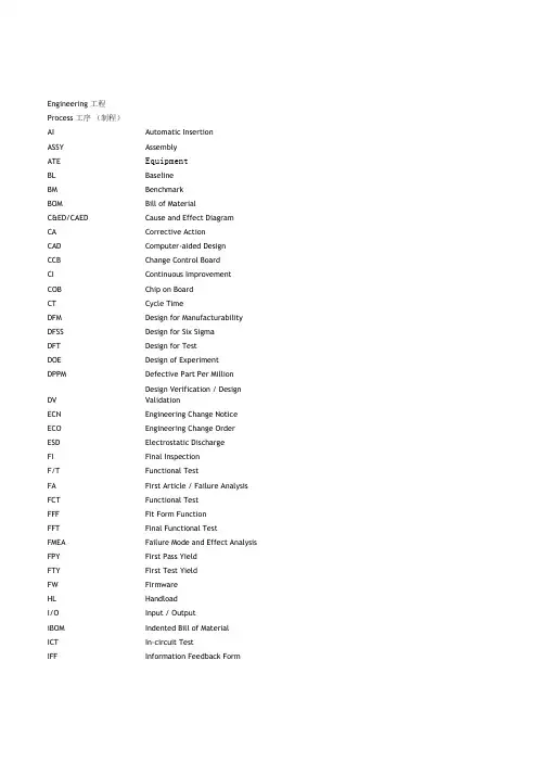
••半导体家园•••技术论坛••••产业动态•半导体公司名录•Automation•半导体厂务•求职招聘•芯片与系统•IC Design•IC Layout•设计验证•EDA技术•设计与制造•工艺整合•Lithography•Etching•Diffusion•Thin Film•CMP•度量检测•晶片制备•封装设计•封装仿真•封装工艺•封装设备•封装材料•封装原理•SMT表面贴装•PCB印刷电路板•Cp&Final Test•测试理论•测试设备•Test Board•Reliability•失效分析•MEMS专区•FPD平板显示器专区•LED半导体照明•太阳能光伏•品质管理•生产管理•供应商管理•人力资源•财务管理•机密管理•市场开发及客户管理•半导体公司创建•设备&工具供求区•原料&耗材供求区•制造加工供求区•元器件供求区•其他服务供求区•闲聊灌水•美图世界•足行天下•健康养生•英文互动•商学院•投资理财您的位置:半导体技术天地>> 首页>> 封装原理>> 查看帖子字体: 小中大设备管理中常用的英文简写代表的意思(很多哦)KEJIAN 发表于: 2009-2-23 13:18 来源: 半导体技术天地Abbreviations and their explanations 缩写与其解释Engineering 工程/ Process 工序(制程)4M&1EMan, Machine, Method, Material, Environment人,机器,方法,物料,环境- 可能导致或造成问题的根本原因AIAutomatic Insertion自动插机ASSYAssembly制品装配ATEAutomatic Test Equipment自动测试设备BLBaseline参照点BMBenchmark参照点BOMBill of Material生产产品所用的物料清单C&ED/CAEDCause and Effect Diagram原因和效果图CACorrective Action解决问题所采取的措施CADComputer-aided Design电脑辅助设计.用于制图和设计3维物体的软件CCBChange Control Board对文件的要求进行评审,批准,和更改的小组CIContinuous Improvement依照短期和长期改善的重要性来做持续改善COBChip on Board邦定-线焊芯片到PCB板的装配方法.CTCycle Time完成任务所须的时间DFMDesign for Manufacturability产品的设计对装配的适合性DFMEADesign Failure Mode and Effect Analysis设计失效模式与后果分析--在设计阶段预测问题的发生的可能性并且对之采取措施DFSSDesign for Six Sigma六西格玛(6-Sigma)设计-- 设计阶段预测问题的发生的可能性并且对之采取措施并提高设计对装配的适合性DFTDesign for Test产品的设计对测试的适合性DOEDesign of Experiment实验设计-- 用于证明某种情况是真实的DPPMDefective Part Per Million根据一百万件所生产的产品来计算不良品的标准DVDesign Verification / Design Validation设计确认ECNEngineering Change Notice客户要求的工程更改或内部所发出的工程更改文件ECOEngineering Change Order客户要求的工程更改ESDElectrostatic Discharge静电发放-由两种不导电的物品一起摩擦而产生的静电可以破坏ICs和电子设备FIFinal Inspection在生产线上或操作中由生产操作员对产品作最后检查Functional Test测试产品的功能是否与所设计的一样FAFirst Article / Failure Analysis首件产品或首件样板/ 产品不良分析FCTFunctional Test功能测试-检查产品的功能是否与所设计的一样FFFFit Form Function符合产品的装配,形状和外观及功能要求FFTFinal Functional Test包装之前,在生产线上最后的功能测试FMEAFailure Mode and Effect Analysis失效模式与后果分析-- 预测问题的发生可能性并且对之采取措施FPYFirst Pass Yield首次检查合格率FTYFirst Test Yield首次测试合格率FWFirmware韧体(软件硬化)-控制产品功能的软件HLHandload在波峰焊接之前,将PTH元件用手贴装到PCB上,和手插机相同I/OInput / Output输入/ 输出Indented Bill of Material内部发出的BOM(依照客户的BOM)ICTIn-circuit Test线路测试-- 用电气和电子测试来检查PCBA短路,开路,少件,多件和错件等等不良IFFInformation Feedback Form情报联络书-反馈信息所使用的一种表格IRInfra-red红外线KPIVKey Process Input Variable主要制程输入可变因素-在加工过程中,所有输入的参数/元素,将影响制成品的质量的可变因素KPOVKey Process Output Variable主要制程输出可变因素-在加工过程中,所有输出的结果,所呈现的产品品质特征。
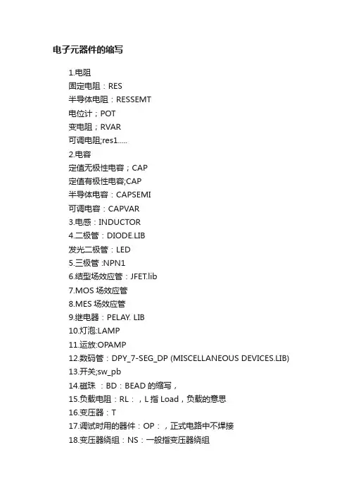
电子元器件的缩写1.电阻固定电阻:RES半导体电阻:RESSEMT电位计;POT变电阻;RVAR可调电阻;res1.....2.电容定值无极性电容;CAP定值有极性电容;CAP半导体电容:CAPSEMI可调电容:CAPVAR3.电感:INDUCTOR4.二极管:DIODE.LIB发光二极管:LED5.三极管 :NPN16.结型场效应管:JFET.lib7.MOS场效应管8.MES场效应管9.继电器:PELAY. LIB10.灯泡:LAMP11.运放:OPAMP12.数码管:DPY_7-SEG_DP (MISCELLANEOUS DEVICES.LIB)13.开关;sw_pb14.磁珠:BD:BEAD的缩写,15.负载电阻:RL:,L指Load,负载的意思16.变压器:T17.调试时用的器件:OP:,正式电路中不焊接18.变压器绕组:NS:一般指变压器绕组19.接插件、U型跳线:JP:原理图常用库文件:Miscellaneous Devices.ddbDallas Microprocessor.ddbIntel Databooks.ddbProtel DOS Schematic Libraries.ddb PCB元件常用库:Advpcb.ddbGeneral IC.ddbMiscellaneous.ddb部分分立元件库元件名称及中英对照AND 与门ANTENNA 天线BATTERY 直流电源BELL 铃,钟BVC 同轴电缆接插件BRIDGE 1 整流桥(二极管)BRIDGE 2 整流桥(集成块)BUFFER 缓冲器BUZZER 蜂鸣器CAP 电容CAPACITOR 电容CAPACITOR POL 有极性电容CAPVAR 可调电容CIRCUIT BREAKER 熔断丝COAX 同轴电缆CON 插口CRYSTAL 晶体整荡器DB 并行插口DIODE 二极管DIODE SCHOTTKY 稳压二极管DIODE VARACTOR 变容二极管DPY_3-SEG 3段LEDDPY_7-SEG 7段LEDDPY_7-SEG_DP 7段LED(带小数点) ELECTRO 电解电容FUSE 熔断器INDUCTOR 电感INDUCTOR IRON 带铁芯电感INDUCTOR3 可调电感JFET N N沟道场效应管JFET P P沟道场效应管LAMP 灯泡LAMP NEDN 起辉器LED 发光二极管METER 仪表MICROPHONE 麦克风MOSFET MOS管MOTOR AC 交流电机MOTOR SERVO 伺服电机NAND 与非门NOR 或非门NOT 非门NPN NPN三极管NPN-PHOTO 感光三极管OPAMP 运放OR 或门PHOTO 感光二极管PNP 三极管NPN DAR NPN三极管PNP DAR PNP三极管POT 滑线变阻器PELAY-DPDT 双刀双掷继电器RES1.2 电阻RES3.4 可变电阻RESISTOR BRIDGE 桥式电阻RESPACK 电阻SCR 晶闸管PLUG ? 插头PLUG AC FEMALE 三相交流插头SOCKET 插座SOURCE CURRENT 电流源SOURCE VOLTAGE 电压源SPEAKER 扬声器SW 开关SW-DPDY 双刀双掷开关SW-SPST 单刀单掷开关SW-PB 按钮THERMISTOR 电热调节器TRANS1 变压器TRANS2 可调变压器TRIAC 三端双向可控硅TRIODE 三极真空管VARISTOR 变阻器ZENER 齐纳二极管DPY_7-SEG_DP 数码管SW-PB 开关其他元件库Protel Dos Schematic 4000 Cmos .Lib (40.系列CMOS管集成块元件库)4013 D 触发器4027 JK 触发器Protel Dos Schematic Analog Digital.Lib(模拟数字式集成块元件库)AD系列 DAC系列 HD系列 MC系列Protel Dos Schematic Comparator.Lib(比较放大器元件库)Protel Dos Shcematic Intel.Lib(INTEL公司生产的80系列CPU 集成块元件库)Protel Dos Schematic Linear.lib(线性元件库)Protel Dos Schemattic Memory Devices.Lib(内存存储器元件库)Protel Dos Schematic SYnertek.Lib(SY系列集成块元件库)Protes Dos Schematic Motorlla.Lib(摩托罗拉公司生产的元件库)Protes Dos Schematic NEC.lib(NEC公司生产的集成块元件库)Protes Dos Schematic Operationel Amplifers.lib(运算放大器元件库)Protes Dos Schematic TTL.Lib(晶体管集成块元件库 74系列)Protel Dos Schematic Voltage Regulator.lib(电压调整集成块元件库)Protes Dos Schematic Zilog.Lib(齐格格公司生产的Z80系列CPU集成块元件库)元件属性对话框中英文对照Lib ref 元件名称Footprint 器件封装Designator 元件称号Part 器件类别或标示值Schematic Tools 主工具栏Writing T ools 连线工具栏Drawing Tools 绘图工具栏部分分立元件库元件名称及中英对照Power Objects 电源工具栏Digital Objects 数字器件工具栏Simulation Sources 模拟信号源工具栏PLD Toolbars 映象工具栏7407 驱动门1N914 二极管74Ls00 与非门74LS04 非门74LS08 与门74LS390 TTL 双十进制计数器7SEG 4针BCD-LED 输出从0-9 对应于4 根线的BCD码7SEG 3-8 译码器电路BCD-7SEG[size=+0]转换电路ALTERNATOR 交流发电机AMMETER-MILLI mA安培计AND 与门BATTERY 电池/电池组BUS 总线CAP 电容CAPACITOR 电容器CLOCK 时钟信号源CRYSTAL 晶振D-FLIPFLOP D 触发器FUSE 保险丝GROUND 地LAMP 灯LED-RED 红色发光二极管LOGIC ANALYSER 逻辑分析器LOGICPROBE 逻辑探针LOGICPROBE[BIG] 逻辑探针用来显示连接位置的逻辑状态LOGICSTATE 逻辑状态用鼠标点击,可改变该方框连接位置的逻辑状态LOGICTOGGLE 逻辑触发MASTERSWITCH 按钮手动闭合,立即自动打开MOTOR 马达OR 或门POT-LIN 三引线可变电阻器POWER 电源RES 电阻RESISTOR 电阻器SWITCH 按钮手动按一下一个状态SWITCH-SPDT 二选通一按钮VOLTMETER 伏特计VOLTMETER-MILLI mV伏特计VTERM 串行口终端Electromechanical 电机Inductors 变压器Laplace Primitives 拉普拉斯变换Memory IcsMicroprocessor IcsMiscellaneous 各种器件AERIAL-天线;ATAHDD;ATMEGA64;BATTERY;CELL;CRYSTAL-晶振;FUSE;METER-仪表;Modelling Primitives 各种仿真器件是典型的基本元器模拟,不表示具体型号,只用于仿真,没有PCBOptoelectronics 各种发光器件发光二极管,LED,液晶等等PLDs & FPGAsResistors 各种电阻Simulator Primitives 常用的器件Speakers & SoundersSwitches & Relays开关,继电器,键盘Switching Devices 晶阊管Transistors 晶体管(三极管,场效应管)TTL 74 seriesTTL 74ALS seriesTTL 74AS seriesTTL 74F seriesTTL 74HC seriesTTL 74HCT seriesTTL 74LS seriesTTL 74S seriesAnalog Ics 模拟电路集成芯片Capacitors 电容集合CMOS 4000 seriesConnectors 排座,排插Data Converters ADC,DACDebugging Tools 调试工具ECL 10000 SeriesAND 与门ANTENNA 天线BATTERY 直流电源BELL 铃,钟BVC 同轴电缆接插件BRIDEG 1 整流桥(二极管) BRIDEG 2 整流桥(集成块) BUFFER 缓冲器BUZZER 蜂鸣器CAP 电容CAPACITOR 电容CAPACITOR POL 有极性电容CAPVAR 可调电容CIRCUIT BREAKER 熔断丝COAX 同轴电缆CON 插口CRYSTAL 晶体整荡器DB 并行插口DIODE 二极管DIODE SCHOTTKY 稳压二极管DIODE VARACTOR 变容二极管DPY_3-SEG 3 段LEDDPY_7-SEG 7 段LEDDPY_7-SEG_DP 7 段LED(带小数点) ELECTRO 电解电容FUSE 熔断器INDUCTOR 电感INDUCTOR IRON 带铁芯电感INDUCTOR3 可调电感JFET N N 沟道场效应管JFET P P沟道场效应管LAMP 灯泡LAMP NEDN 起辉器LED 发光二极管METER 仪表MICROPHONE 麦克风MOSFETMOS管MOTOR AC 交流电机MOTOR SERVO 伺服电机NAND 与非门NOR 或非门NOT 非门NPN NPN 三极管NPN-PHOTO 感光三极管OPAMP 运放OR 或门PHOTO 感光二极管Device.lib 包括电阻、电容、二极管、三极管和PCB的连接器符号ACTIVE.LIB 包括虚拟仪器和有源器件DIODE.LIB 包括二极管和整流桥DISPLAY.LIB 包括 LCD、LEDBIPOLAR.LIB 包括三极管FET.LIB 包括场效应管ASIMMDLS.LIB 包括模拟元器件VALVES .LIB 包括电子管ANALOG.LIB 包括电源调节器、运放和数据采样IC CAPACITORS.LIB 包括电容COMS.LIB 包括 4000 系列ECL.LIB 包括 ECL10000 系列OPAMP.LIB 包括运算放大器RESISTORS.LIB 包括电阻FAIRCHLD .LIB 包括 FAIRCHLD 半导体公司的分立器件LINTEC.LIB 包括 LINTEC 公司的运算放大器NATDAC.LIB 包括国家半导体公司的数字采样器件NATOA.LIB 包括国家半导体公司的运算放大器TECOOR.LIB 包括TECOOR公司的SCR 和TRIACTEXOAC.LIB 包括德州仪器公司的运算放大器和比较器PNP 三极管NPN DAR NPN 三极管PNP DAR PNP三极管POT 滑线变阻器PELAY-DPDT 双刀双掷继电器RES1.2 电阻RES3.4 可变电阻RESISTOR BRIDGE ? 桥式电阻RESPACK ? 电阻SCR 晶闸管PLUG 插头PLUG AC FEMALE 三相交流插头SOCKET 插座SOURCE CURRENT 电流源SOURCE VOLTAGE 电压源SPEAKER 扬声器SW 开关SW-DPDY 双刀双掷开关SW-SPST 单刀单掷开关SW-PB 按钮THERMISTOR 电热调节器TRANS1 变压器TRANS2 可调变压器TRIAC 三端双向可控硅TRIODE 三极真空管VARISTOR 变阻器ZENER 齐纳二极管DPY_7-SEG_DP 数码管SW-PB 开关序号英文简写元件英文名元件中文名1 Res semi Semiconductor Resistor 半导体电阻2 Cap semi Semiconductor Capacitor 半导体电容器3 Cap Var Variable or AdjustableCapacitor可变或可调电容4 Cap Pol1 Polarized Capacitor (Radial) 极化电容(径向)5 Cap Pol2 Polarized Capacitor (Axial) 极化电容(轴向)6 Cap Capacitor 电容(径向)7 Cap Pol3 Polarized Capacitor (SurfaceMount)极化电容(表面贴装)8 Cap Feed Feed-Through Capacitor 馈通电容9 Cap2 Capacitor 电容10 ResVaristorVaristor (Voltage-SensitiveResistor)压敏电阻(电压敏感电阻)11 Res Tap Tapped Resistor 抽头电阻12 Res Thermal T hermal Resistor 热敏电阻13 Rpot Potentiometer Resistor (侧调或顶调)电位器14 Rpot SM Square Trimming Potentiometer (顶调)方形电位器15 Res Bridge Resistor Bridge 电阻桥16 Bridge1 Full Wave Diode Bridge 整流桥17 Bridge2 Bridge Rectifier 整流桥集成组件(比1封装较大)18 Res Adj Variable Resistor 可变电阻19 Res3 Resistor IPC的高密度贴片电阻20 D Tunnel2 Tunnel Diode - Dependent SourceModel隧道二极管 - 依赖源模型21 D Varactor Variable Capacitance Diode 变容二极管22 D Schottky Schottky Diode 肖特基二极管23 Diode1N54023 Amp General Purpose Rectifier 3放大器通用整流器其中,cap,cap2,cap pol1和cap pol2分别如下图所示:有极性电容为电解电容,无极性电容为普通电容,电解电容的容量一般比普通电容的大,在滤波时电解电容用于滤低频,普通电容用于滤高频。
半导体行业各品牌名称、缩写、中文名、总部
全名流行缩写官方中文名总部MediaTek MTK 联发科台湾Princeton PTC 普诚科技台湾Richtek / 立崎台湾Sunplus / 凌阳台湾Anapec 茂达台湾EUTech 德信台湾Realtek 瑞煜台湾Winbond 华邦台湾VIA 威盛台湾
日本半导体厂家
EPSON 爱普生日本Fujitsu 富士通日本NEC 日电日本OKI 冲电子日本 ROHM 罗姆日本Renesas 瑞萨日本SHARP 夏普日本Seiko NPC 精工日本YAMAHA 雅马哈日本Toshiba 东芝日本RICOH 理光日本TOREX 特瑞仕日本mitsubishi 三菱日本Sanyo 三洋日本AKM / 日本
韩国半导体厂家
Samsung 三星韩国Corelogic / 韩国Hynix 海力士韩国LG 乐金韩国Atlab / 韩国
美国半导体厂家
Analog Device ADI 模拟器件美国Agere System 杰尔美国Agilent 安捷伦美国AMD/Spansion / 美国Atmel 爱特梅尔美国。
半导体集成电路常见封装缩写解释1. DIP(dual in-line PACkage)双列直插式封装。
插装型封装之一,引脚从封装两侧引出,封装材料有塑料和陶瓷两种。
DIP 是最普及的插装型封装,应用范围包括标准逻辑IC,存贮器LSI,微机电路等。
引脚中心距2.54mm,引脚数从6 到64。
封装宽度通常为15.2mm。
有的把宽度为7.52mm 和10.16mm 的封装分别称为skinny DIP 和slim DIP(窄体型DIP)。
但多数情况下并不加区分,只简单地统称为DIP。
另外,用低熔点玻璃密封的陶瓷DIP 也称为Cerdip(见Cerdip)。
BGA是英文Ball Grid Array Package的缩写,即球栅阵列封装。
SOP小型外引脚封装Small Outline Package JSSOP收缩型小外形封装Shrink Small Outline Package P与SOP的区别:近似小外形封装,但宽度要比小外形封装更窄,可节省组装面积的新型封装。
2. DIP(dual tape carrier PACkage)同上。
日本电子机械工业会标准对DTCP 的命名(见DTCP)。
QTCP(quad tape carrier PACkage)四侧引脚带载封装。
TCP 封装之一,在绝缘带上形成引脚并从封装四个侧面引出。
是利用TAB 技术的薄型封装(见TAB、TCP)。
COB(chip on board)板上芯片封装,是裸芯片贴装技术之一,半导体芯片交接贴装在印刷线路板上,芯片与基板的电气连接用引线缝合方法实现,芯片与基板的电气连接用引线缝合方法实现,并用树脂覆盖以确保可靠性。
虽然COB 是最简单的裸芯片贴装技术,但它的封装密度远不如TAB 和倒片焊技术。
JLCC(J-leaded chip carrier)J 形引脚芯片载体。
指带窗口CLCC 和带窗口的陶瓷QFJ 的别称(见CLCC 和QFJ)。
MFG 常用英文单字Semiconductor半导体导体、绝缘体和半导体主要依据导电系数的大小,决定了电子的移动速度。
导体:金、银、铜、铁、人、水……导电系数大,传导绝缘体:塑料、木头、皮革、纸……导电系数小、传导不半导体:硅中加锗、砷、镓、磷……平时不导电加特定电压后导电Wafer 芯片或晶圆:原意为法国的松饼,饼干上有格子状的饰纹,与FAB内生产的芯片图形类Lot 批;一批芯片中最多可以有25片,最少可以只有一片。
ID Identification的缩写。
用以辨识各个独立的个体,就像公司内每一个人有自己的识别证。
Wafer ID 每一片芯片有自己的芯片刻号,叫Wafer ID。
Lot ID 每一批芯片有自己的批号,叫Lot ID。
Part ID 各个独立的批号可以共享一个型号,叫Part ID。
WIP Work In Process,在制品。
从芯片投入到芯片产品,FAB内各站积存了相当数量的芯片,统称为FAB内的WIP 。
一整个制程又可细分为数百个Stage和Step,每一个Stage所堆积的芯片,称为Stage WIP。
Lot Priority 每一批产品在加工的过程中在WIP中被选择进机台的优先级。
Super Hot Run的优先级为1,视为等级最高,必要时,当Lo上一站加工时,本站便要空着机台等待Super Hot RuHot Run的优先级为2,紧急程度比Super Hot Run次一级。
Normal的优先级为3,视为正常的等级,按正常的派货原则视常班向生产指令而Cycle time 生产周期,FAB Cycle Time 定义为:从芯片投入到芯片产生的这一段时间。
Stage Cycle Time:Lot从进站等候开始到当站加工后出货时间点截Spec. 规格Specification的缩写。
产品在机台加工过程中,每一站均设定规格。
机台加工后,产品或控片经由量测机台量测,该产品加工后,是否在规格内。
MFG 常用英文单字Semiconductor半导体导体、绝缘体和半导体主要依据导电系数的大小,决定了电子的移动速度。
导体:金、银、铜、铁、人、水……导电系数大,传导容易绝缘体:塑料、木头、皮革、纸……导电系数小、传导不容易半导体:硅中加锗、砷、镓、磷……平时不导电加特定电压后导电Wafer 芯片或晶圆:原意为法国的松饼,饼干上有格子状的饰纹,与FAB内生产的芯片图形类似。
Lot 批;一批芯片中最多可以有25片,最少可以只有一片。
ID Identification的缩写。
用以辨识各个独立的个体,就像公司内每一个人有自己的识别证。
Wafer ID 每一片芯片有自己的芯片刻号,叫Wafer ID。
Lot ID 每一批芯片有自己的批号,叫Lot ID。
Part ID 各个独立的批号可以共享一个型号,叫Part ID。
WIP Work In Process,在制品。
从芯片投入到芯片产品,FAB内各站积存了相当数量的芯片,统称为FAB内的WIP 。
一整个制程又可细分为数百个Stage和Step,每一个Stage所堆积的芯片,称为Stage WIP。
Lot Priority 每一批产品在加工的过程中在WIP中被选择进机台的优先级。
Super Hot Run的优先级为1,视为等级最高,必要时,当Lot在上一站加工时,本站便要空着机台等待Super Hot Run。
Hot Run的优先级为2,紧急程度比Super Hot Run次一级。
Normal的优先级为3,视为正常的等级,按正常的派货原则,或视常班向生产指令而定。
Cycle time 生产周期,FAB Cycle Time 定义为:从芯片投入到芯片产生的这一段时间。
Stage Cycle Time:Lot从进站等候开始到当站加工后出货时间点截止。
Spec. 规格Specification的缩写。
产品在机台加工过程中,每一站均设定规格。
机台加工后,产品或控片经由量测机台量测,该产品加工后,是否在规格内。
专业术语1 Active Area 主动区(工作区)主动晶体管(ACTIVE TR ANSISTOR)被制造的区域即所谓的主动区(ACTI VE AREA)。
在标准之MOS制造过程中ACTIVE AREA是由一层氮化硅光罩即等接氮化硅蚀刻之后的局部场区氧化所形成的,而由于利用到局部场氧化之步骤,所以ACTI VE AREA会受到鸟嘴(BIRD’S BEAK)之影响而比原先之氮化硅光罩所定义的区域来的小,以长0.6UM之场区氧化而言,大概会有0.5UM之BIRD’S BEAK 存在,也就是说ACTIVE AREA比原在之氮化硅光罩所定义的区域小0.5UM。
2 ACTONE 丙酮 1. 丙酮是有机溶剂的一种,分子式为CH3COCH3。
2. 性质为无色,具刺激性及薄荷臭味之液体。
3. 在FAB内之用途,主要在于黄光室内正光阻之清洗、擦拭。
4. 对神经中枢具中度麻醉性,对皮肤黏膜具轻微毒性,长期接触会引起皮肤炎,吸入过量之丙酮蒸汽会刺激鼻、眼结膜及咽喉黏膜,甚至引起头痛、恶心、呕吐、目眩、意识不明等。
5. 允许浓度1000PPM。
3 ADI 显影后检查 1.定义:After Developing Inspection 之缩写2.目的:检查黄光室制程;光阻覆盖→对准→曝光→显影。
发现缺点后,如覆盖不良、显影不良…等即予修改,以维护产品良率、品质。
3.方法:利用目检、显微镜为之。
4 AEI 蚀刻后检查 1. 定义:AEI即After Etching Inspection,在蚀刻制程光阻去除前及光阻去除后,分别对产品实施全检或抽样检查。
2.目的:2-1提高产品良率,避免不良品外流。
2-2达到品质的一致性和制程之重复性。
2-3显示制程能力之指针2-4阻止异常扩大,节省成本3.通常AEI检查出来之不良品,非必要时很少作修改,因为重去氧化层或重长氧化层可能造成组件特性改变可靠性变差、缺点密度增加,生产成本增高,以及良率降低之缺点。
单片机常见英文缩写(二)引言概述:本文将介绍一些与单片机相关的常见英文缩写。
这些缩写是在单片机领域中使用较为频繁的,了解并熟练运用这些缩写有助于我们更好地理解和应用单片机技术。
正文内容:一、单片机内部组成1.1 MCU:Microcontroller Unit,意为微控制器单元,是指能够完成微处理器和外围器件集成在一块芯片上的单片机。
1.2 CPU:Central Processing Unit,中央处理器,是单片机内部用来执行指令和处理数据的核心部件。
1.3 RAM:Random Access Memory,随机存储器,是单片机内部用来存储数据和程序的临时存储器件。
1.4 ROM:Read-Only Memory,只读存储器,是单片机内部用来存储程序固化后的指令和数据的非易失性存储器件。
1.5 Flash:一种可擦写和重新编程的存储器技术,常用于单片机中存储程序代码。
二、通信相关缩写2.1 UART:Universal Asynchronous Receiver and Transmitter,通用异步收发器,是常用的串行通信接口。
2.2 SPI:Serial Peripheral Interface,串行外围接口,是一种用于单片机和外围设备之间进行通信的接口协议。
2.3 I2C:Inter-Integrated Circuit,集成电路互联总线,是一种常用的串行通信协议,用于连接多个设备。
2.4 CAN:Controller Area Network,控制器局域网,是一种广泛应用于汽车、工控等领域的串行通信协议。
2.5 USB:Universal Serial Bus,通用串行总线,是一种用于连接计算机和外围设备的通信接口标准。
三、外设和模块缩写3.1 ADC:Analog-to-Digital Converter,模数转换器,用来将模拟信号转换为数字信号的电路。
3.2 PWM:Pulse Width Modulation,脉宽调制技术,用于控制模拟电路的输出功率。
半导体行业术语1 Active Area 主动区(工作区)主动晶体管(ACTIVE TRANSISTOR)被制造的区域即所谓的主动区(ACTIVE AREA)。
在标准之MOS制造过程中ACTIVE AREA是由一层氮化硅光罩即等接氮化硅蚀刻之后的局部场区氧化所形成的,而由于利用到局部场氧化之步骤,所以AC TIVE AREA会受到鸟嘴(BIRD’S BEAK)之影响而比原先之氮化硅光罩所定义的区域来的小,以长0.6UM之场区氧化而言,大概会有0.5UM之BIRD’S BEAK存在,也就是说ACTIVE ARE A比原在之氮化硅光罩所定义的区域小0.5UM。
2 ACTONE 丙酮1. 丙酮是有机溶剂的一种,分子式为CH3COCH3。
2. 性质为无色,具刺激性及薄荷臭味之液体。
3. 在FAB内之用途,主要在于黄光室内正光阻之清洗、擦拭。
4.对神经中枢具中度麻醉性,对皮肤黏膜具轻微毒性,长期接触会引起皮肤炎,吸入过量之丙酮蒸汽会刺激鼻、眼结膜及咽喉黏膜,甚至引起头痛、恶心、呕吐、目眩、意识不明等。
5. 允许浓度1000PPM。
3 ADI 显影后检查1.定义:After Developing Inspection 之缩写2.目的:检查黄光室制程;光阻覆盖→对准→曝光→显影。
发现缺点后,如覆盖不良、显影不良…等即予修改,以维护产品良率、品质。
3.方法:利用目检、显微镜为之。
4 AEI 蚀刻后检查1. 定义:AEI即After Etching Inspection,在蚀刻制程光阻去除前及光阻去除后,分别对产品实施全检或抽样检查。
2.目的:2-1提高产品良率,避免不良品外流。
2-2达到品质的一致性和制程之重复性。
2-3显示制程能力之指针2-4阻止异常扩大,节省成本3.通常AEI检查出来之不良品,非必要时很少作修改,因为重去氧化层或重长氧化层可能造成组件特性改变可靠性变差、缺点密度增加,生产成本增高,以及良率降低之缺点。
CUP Centra l Utilit y Plant中央動力廠房GEX Genera l EXhaus t 普通及熱排氣SEX Scrubb er EXhaus t 酸排氣VEX Volati le orgaic compou nd EXhaus t 有機溶劑排氣AEX Ammoni a EXhaus t 鹼性排氣PCW PlantCoolin g Water工藝冷卻水PV Proces s Vacuum工藝真空HV HouseVacuum真空吸塵CW City Water自來水FMCS Failit y Monito ringContro System廠務監控系統MCC MotorContro l Center馬達控制中心VFD Variab le Freque ncy Device變頻器CCTV CloseCircui t Televs ion 閉路電視PA Public Adress system廣播系統FA Fire Alarm system火災報警系統UPW UltraPure Water超純水FWW Fluori de WasteWater低濃度氫氟酸廢水IWW Indust ry WasteWater工業廢水OWW Organi c WasteWater有機溶劑廢水DAHW DrainAmonia Hydrid e Waste含氨廢水RCL Recycl e water製程回收循環水RCM Reclai m water製程回收再利用水HFW High Fluori de Wastewater高濃度氫氟酸廢水BGW Backgr iding Wastewater晶背研磨廢水SAW Sulfur ic Acid Wastewater硫酸廢液PAW Phosph oricAcid Wastewater磷酸廢液SW Stripp er Wastewater剝離液廢液TW Thinne r Wastewater清洗廢液PIX Pix wastewaterPIX廢液SLOW Oxideslurry wastewater介電質研磨廢水SLWP Metalslurry wastewater金屬研磨廢水SLWP Poly slurry wastewater多晶硅研磨廢水PN2 Proces s N2 製程用氮氣GN2 Genera l N2 一般用氮氣CDA Compre ssor Dry Air 壓縮乾燥空氣VMB ValveManifo ld Box 閥箱空調系統AHU Air Handli ng Unit 空调箱MAU Make-up Air Unit 外气空调箱VAV Variab le Air Volume box 可变风量风箱FFU Fan Filter Unit 风车过滤器HEPA High Effici encyPartic ulate Filter高效率过滤器ULP A UltraLow Penetr ation Filter超高效率过滤器A/S Air Shower空气浴尘室CUP Centra l Utilit y Plant中央動力廠房電力系統FMCS Failit y Monito ringContro l System廠務監控系統MCC MotorContro l Center馬達控制中心VFD Variab le Freque ncy Device變頻器CCTV CloseCircui t Televs ion 閉路電視SCADASuperv isory Contro l And Data Acquis ition监视控制和数据搜集系M CC MotorContro l Center馬達控制中心VFD Variab le Freque ncy Device變頻器水處理系統UPW UltraPure Water超純水RO Revers e Osmosi s 逆滲透膜TOC TotalOrgani c Carbon總有機碳MB MixedBed 混床UF UltraF iltra tion超濾SC Strong Cation強陽離子SA Strong Anion強陰離子WA Weak Anion弱陰離子DO Dissol ved Oxygen溶解氧MD Membra ne Degasi fy 脫氣膜GF Gravit y Filter重力式過濾器.DI Deioni ze 去離子水氣體/化學系統CQC Contin uous Qualit y Contro l连续品质控制系统VMB ValveManifo ld Box 閥箱VMP ValveManifo ld Panel閥盘GMS Gas Monito ringSystem气体监测系统CDS Chemic al Dispen se System化學系统SDS Slurry Dispen se System化學研磨系统环境安全卫生ESH Enviro nment Safety Health环境安全卫生SCBA Self Contai ned Brathi ng Appara tus 自给式空气呼吸器 HVACAHU Air Handli ng Unit 空调箱MAU Make-up Air Unit 外气空调箱VAV Variab le Air Volume box 可变风量风箱FD Fire Damper防火风门FSD combin ed Fire Smoke Damper防火防烟风门SD Smoke Damper防烟风门PHX Plated type Heat Exange r 板式热交换器FFU Fan Filter Unit 风车过滤器HEPA High Effici encyPartic ulate Filter高效率过滤器ULPA UltraLow Penetr ation Filter超高效率过滤器A/S Air Shower空气浴尘室A/L Air Lock 气闭门室DCC Dry Coolin g Coil 干盤管FCU Fan Coil Unit 小型冷风机SF SmokeFan 消防排烟风车EF Exhaus t Fan 通风排气风车CUP Centra l Utilit y Plant中央動力廠房GEX Genera l EXhaus t 普通及熱排氣SEX Scrubb er EXhaus t 酸排氣VEX Volati le orgaic compou nd EXhaus t 有機溶劑排氣AEX Ammoni a EXhaus t 鹼性排氣PCW Proces s Coolin g Water工藝冷卻水PV PlantVacuum工藝真空HV HouseVacuum真空吸塵CW City Water自來水FMCS Failit y Monito ringContro l System廠務監控系統MCC MotorContro l Center馬達控制中心VFD Variab le Freque ncy Device變頻器CCTV CloseCircui t Televs ion 閉路電視PA Public Adress system廣播系統FA Fire Alarm system火災報警系統UPW UltraPure Water超純水RO revers e Osmosi s 逆滲透膜TOC total organi c carbon總有機碳MB mixedbed 混床UF ultraf iltra tion超濾SC strong cation強陽離子SA strong Anion強陰離子WA weak Anion弱陰離子DO dissol ved oxygen溶解氧MD membra ne Degasi fy 脫氣膜GF gravit y Filter重力式過濾器.DI deioni ze 去離子水FWW Fluori de WasteWater低濃度氫氟酸廢水IWW Indust ry WasteWater工業廢水OWW Organi c WasteWater有機溶劑廢水DAHW DrainAmonia Hydrid e Wastew ater含氨廢水RCL Recycl e water製程回收循環水RCM Reclai m water製程回收再利用水HFW High Fluori de Waste高濃度氫氟酸廢液BGW Backgr iding Wastewater晶背研磨廢水SAW Sulfur ic Acid Waste硫酸廢液PAW Phosph oric Acid Waste磷酸廢液SW Stripp er Waste剝離液廢液TW Thinne r Waste清洗廢液PIX PIX wastePIX廢液SL W-O SLurry Wastew aterOxide介電質研磨廢水SLW-M SLurry Wastew aterMetal金屬研磨廢水SLW-P SLurry Wastew aterPoly 多晶硅研磨廢水PN2 Proces s N2 製程用氮氣GN2 Genera l N2 一般用氮氣CDA Compre ssor Dry Air壓縮乾燥空氣VMB ValveManifo ld Box 閥箱ESHESH Enviro nment Safety Health环境安全卫生SCBA Self Contai ned Brathi ng Appara tus 自给式空气呼吸器ISO Intern ation al Organi zatio n for Standa rdiza tion国际标准化组织。
••半导体家园•••技术论坛••••产业动态•半导体公司名录•Automation•半导体厂务•求职招聘•芯片与系统•IC Design•IC Layout•设计验证•EDA技术•设计与制造•工艺整合•Lithography•Etching•Diffusion•Thin Film•CMP•度量检测•晶片制备•封装设计•封装仿真•封装工艺•封装设备•封装材料•封装原理•SMT表面贴装•PCB印刷电路板•Cp&Final Test•测试理论•测试设备•Test Board•Reliability•失效分析•MEMS专区•FPD平板显示器专区•LED半导体照明•太阳能光伏•品质管理•生产管理•供应商管理•人力资源•财务管理•机密管理•市场开发及客户管理•半导体公司创建•设备&工具供求区•原料&耗材供求区•制造加工供求区•元器件供求区•其他服务供求区•闲聊灌水•美图世界•足行天下•健康养生•英文互动•商学院•投资理财您的位置:半导体技术天地>> 首页>> 封装原理>> 查看帖子字体: 小中大设备管理中常用的英文简写代表的意思(很多哦)KEJIAN 发表于: 2009-2-23 13:18 来源: 半导体技术天地Abbreviations and their explanations 缩写与其解释Engineering 工程/ Process 工序(制程)4M&1EMan, Machine, Method, Material, Environment人,机器,方法,物料,环境- 可能导致或造成问题的根本原因AIAutomatic Insertion自动插机ASSYAssembly制品装配ATEAutomatic Test Equipment自动测试设备BLBaseline参照点BMBenchmark参照点BOMBill of Material生产产品所用的物料清单C&ED/CAEDCause and Effect Diagram原因和效果图CACorrective Action解决问题所采取的措施CADComputer-aided Design电脑辅助设计.用于制图和设计3维物体的软件CCBChange Control Board对文件的要求进行评审,批准,和更改的小组CIContinuous Improvement依照短期和长期改善的重要性来做持续改善COBChip on Board邦定-线焊芯片到PCB板的装配方法.CTCycle Time完成任务所须的时间DFMDesign for Manufacturability产品的设计对装配的适合性DFMEADesign Failure Mode and Effect Analysis设计失效模式与后果分析--在设计阶段预测问题的发生的可能性并且对之采取措施DFSSDesign for Six Sigma六西格玛(6-Sigma)设计-- 设计阶段预测问题的发生的可能性并且对之采取措施并提高设计对装配的适合性DFTDesign for Test产品的设计对测试的适合性DOEDesign of Experiment实验设计-- 用于证明某种情况是真实的DPPMDefective Part Per Million根据一百万件所生产的产品来计算不良品的标准DVDesign Verification / Design Validation设计确认ECNEngineering Change Notice客户要求的工程更改或内部所发出的工程更改文件ECOEngineering Change Order客户要求的工程更改ESDElectrostatic Discharge静电发放-由两种不导电的物品一起摩擦而产生的静电可以破坏ICs和电子设备FIFinal Inspection在生产线上或操作中由生产操作员对产品作最后检查Functional Test测试产品的功能是否与所设计的一样FAFirst Article / Failure Analysis首件产品或首件样板/ 产品不良分析FCTFunctional Test功能测试-检查产品的功能是否与所设计的一样FFFFit Form Function符合产品的装配,形状和外观及功能要求FFTFinal Functional Test包装之前,在生产线上最后的功能测试FMEAFailure Mode and Effect Analysis失效模式与后果分析-- 预测问题的发生可能性并且对之采取措施FPYFirst Pass Yield首次检查合格率FTYFirst Test Yield首次测试合格率FWFirmware韧体(软件硬化)-控制产品功能的软件HLHandload在波峰焊接之前,将PTH元件用手贴装到PCB上,和手插机相同I/OInput / Output输入/ 输出Indented Bill of Material内部发出的BOM(依照客户的BOM)ICTIn-circuit Test线路测试-- 用电气和电子测试来检查PCBA短路,开路,少件,多件和错件等等不良IFFInformation Feedback Form情报联络书-反馈信息所使用的一种表格IRInfra-red红外线KPIVKey Process Input Variable主要制程输入可变因素-在加工过程中,所有输入的参数/元素,将影响制成品的质量的可变因素KPOVKey Process Output Variable主要制程输出可变因素-在加工过程中,所有输出的结果,所呈现的产品品质特征。
半导体工艺流程英文缩写Semiconductor process technology plays a crucial role in the fabrication of integrated circuits and other electronic devices. The complexity of semiconductor process technology often results in the use of numerous abbreviations to represent key steps, materials, and equipment. These abbreviations help provide a standardized and concise way of communicating within the semiconductor industry, but they can be overwhelming for those new to the field.半导体工艺技术在集成电路和其他电子设备的制造中起着至关重要的作用。
半导体工艺技术的复杂性往往导致使用大量缩写来代表关键步骤、材料和设备。
这些缩写有助于在半导体行业内进行标准化和简洁的交流,但对于新手来说可能会感到不知所措。
One common set of abbreviations used in semiconductor process technology is related to the different steps involved in the fabrication of a semiconductor device. For example, the process flow may include steps such as thin film deposition (TFD), photolithography (PL), etch (ET), and chemical mechanical planarization (CMP). Each of these steps plays a critical role in defining the features and electricalcharacteristics of the semiconductor device. Understanding these abbreviations is essential for engineers and technicians working in semiconductor fabrication facilities.在半导体工艺技术中常用的一组缩写涉及到半导体器件制造的不同步骤。
芯片,设计\版图,晶圆制造,工艺,制程,封装,测试,wafer,design,fabrication,process,layout,package,test1 Active Area 主动区(工作区)主动晶体管(ACTIVE TRANSISTOR)被制造的区域即所谓的主动区(ACTIVE AREA)。
在标准之MOS制造过程中ACTIVE AREA是由一层氮化硅光罩即等接氮化硅蚀刻之后的局部场区氧化所形成的,而由于利用到局部场氧化之步骤,所以ACTIVE AREA会受到鸟嘴(BIRD’S BEAK)之影响而比原先之氮化硅光罩所定义的区域来的小,以长0.6UM之场区氧化而言,大概会有0.5UM之BIRD’S BEAK存在,也就是说ACTIVE AREA比原在之氮化硅光罩所定义的区域小0.5UM。
2 ACTONE 丙酮1. 丙酮是有机溶剂的一种,分子式为CH3COCH3。
2. 性质为无色,具刺激性及薄荷臭味之液体。
3. 在FAB内之用途,主要在于黄光室内正光阻之清洗、擦拭。
4. 对神经中枢具中度麻醉性,对皮肤黏膜具轻微毒性,长期接触会引起皮肤炎,吸入过量之丙酮蒸汽会刺激鼻、眼结膜及咽喉黏膜,甚至引起头痛、恶心、呕吐、目眩、意识不明等。
5. 允许浓度1000PPM。
3 ADI 显影后检查1.定义:After Developing Inspection 之缩写2.目的:检查黄光室制程;光阻覆盖→对准→曝光→显影。
发现缺点后,如覆盖不良、显影不良…等即予修改,以维护产品良率、品质。
3.方法:利用目检、显微镜为之。
4 AEI 蚀刻后检查1. 定义:AEI即After Etching Inspection,在蚀刻制程光阻去除前及光阻去除后,分别对产品实施全检或抽样检查。
2.目的:2-1提高产品良率,避免不良品外流。
2-2达到品质的一致性和制程之重复性。
2-3显示制程能力之指针2-4阻止异常扩大,节省成本3.通常AEI检查出来之不良品,非必要时很少作修改,因为重去氧化层或重长氧化层可能造成组件特性改变可靠性变差、缺点密度增加,生产成本增高,以及良率降低之缺点。
A/D analog to digitalAA atomic absorptionAAS atomic absorption spectroscopyABC activity-based costingABM activity-based managementAC alternating current; activated carbon ACF anisotropic conductive filmACI after-clean inspectionACP anisotropic conductive pasteACT alternative control techniques; actual cycle timeADC analog-to-digital converterADE advanced development environmentADI after-develop inspectionADT applied diagnostic techniqueADTSEM Apply/Develop Track Specific Equipment ModelAE atomic emission; acousticemission; absolute ellipsometryAEC advanced equipment controllerAECS Advanced Equipment ControlSystem; Automated Equipment Control SystemAEI after-etch inspection; automated equipment interfaceAEM analytical electron microscopyAES Auger emission/electron spectroscopyAFM atomic force microscopyAFP abrasive-free polishAg silverA-GEMTF Advanced GEM Task ForceAGV automated guided vehicleAHF anhydrous hydrogen fluorideAHU air handling unitAIR automated image retrievalAl aluminumALD atomic layer depositionALE atomic layer epitaxy; application logic elementALS advanced light source; advanced low-power SchottkyAMC airborne molecular contamination AMHS automated material handling system AMT advanced manufacturing technology AMU atomic mass unitANN artificial neural networkANOVA analysis of varianceAOV air-operated valveAP adhesion promoterAPA advanced performance algorithmAPC advanced process controlAPCD add-on pollution control deviceAPCFI Advanced Process Control Framework Initiative APCVD atmospheric pressure chemical vapor deposition APEC advanced process equipment controlAPI application programming interface; atmospheric pressure ionizationAPM atmospheric passivation module; acoustic plate modeAPRDL Advanced Products Research and Development LaboratoryaPSM attenuating phase-shift maskAQI ACCESS query interfaceAQL acceptable quality levelAr argonAR aspect ratioARAMS Automated ReliabilityARC antireflective coatingARDE aspect ratio-dependent etchingARPA Advanced Research Projects Agency (see DARPA) ARS angle-resolved scatteringAs arsenicAS/RS automated storage and retrieval systemASAP Advanced Stepper Application ProgramASIC application-specific integrated circuitASO automatic shutoffASP advanced strip and passivation; advanced strip processorASR automated send receiveATDF Advanced ToolDevelopment FacilityATE automatic test equipmentATG automatic test generationATLAS abbreviated test language for all systems atm atmosphereATP advanced technology program; adenosine triphosphate; acceptance and tool performanceATR attenuated total reflectance Att attenuatedAu goldAVP advanced vertical processor AVS advanced visualization systemAWE asymptotic waveform evaluationAWISPM above wafer in situ particle monitoringAWS advanced wet stationB billion; boronBa bariumBARC bottom antireflective coatingBASE Boston Area Semiconductor Education (Council) BAW bulk acoustic waveBC bias contrastBDEV behavior-level deviationBDS Brownian Dynamics SimulationBe berylliumBEOL back end of lineBESOI bonded and etchback silicon on insulatorBF brightfieldBFGS Broyden-Fletcher- Goldfarb-Shanno optimization algorithmBFL buffered field-effect transistor logicBGA ball grid arrayBHT Brinell hardness testBi bismuthBiCMOS bipolar complementary metal-oxide semiconductor BIFET bipolar field-effect transistorBIM binary intensity maskBiMOS bipolar metal-oxide semiconductorBIST built-in self-testBIT bulk ion temperatureBITE built-in test equipmentBMC bubble memory controllerBMD bulk micro defectBOE buffered oxide etchantBOR bottom of rangeBOSS Book of SEMI Standards; binary object storage systemBOX buried oxideBPR beam profile reflectometry; business process reengineeringBPSG boron phosphosilicate glass BPTEOS BPSG from a TEOS sourceBr bromineBSE backscattered electron detection BTAB bumped tape automated bonding BV breakdown voltageC carbonCa calciumCA CIM architectureCAA CIM applications architectureCAB Competitive Analysis BenchmarkingCAD computer-aided designCADT control application development toolCAE computer-aided engineeringCAI computer-assisted instructionCAM computer-aided manufacturingCAPS computer-assisted problem solvingCAR chemically amplified resistCARRI Computerized Assessment of Relative Risk ImpactsCASE computer-aided softwareengineering; computer-aided systems engineeringCAT computer-aided testingCAW Construction Analysis Workgroup CAWC cryogenic aerosol wafer cleaning CBGA ceramic ball grid arrayCBS chemical bottle storage areaCBT computer-based trainingCC chip carrier; cluster controller CCC ceramic chip carrierCCD charge-coupled deviceCCSL compatible current-sinking logic CCW counterclockwiseCd cadmiumCD critical dimensionCD/OL critical dimension overlayCDA clean dry airCDE chemical downstream etchCDEM Customer Delivery Enterprise Model CDI collector-diffusion isolation CDM Common Device Model for SABCDO controlled decomposition/oxidation CDR chemical distribution roomCDS chemical distribution systemCe ceriumCE capillary electrophoresisCEC cell evaluation chipCEE control execution environment CEM continuous emissions monitoring CER-DIP ceramic dual in-line packageCFA component failure analysisCFC chlorofluorocarbonCFD computational fluid dynamics CFM contamination-free manufacturing CIC cleanroom interface chamberCID charge-injection deviceCIE computer-integrated engineering CIM computer-integrated manufacturingCIM-OSA computer-integrated manufacturing-open systems architecture (ESPRIT program)CIP Continuous Improvement ProgramCIS Center for Integrated SystemsCISC complex instruction set computerCl chlorineCLCC ceramic leaded chip carrierCLIC closed-loop intensity controlCM configuration management; cassette module CMC cassette module controllerCML current mode logicCMM capability maturity modelCMOS complementary metal-oxide semiconductorCMP chemical mechanical planarizationCMR common-mode rejection ratio; cancel move requestCNC computer numerical control; condensation nucleus counterCNT carbon nanotubeCo cobaltCOB chip-on-boardCOC cost of consumablesCODEC coder-decoderCOED computer-optimized experimental design COGS cost of goods soldCoO cost of ownershipCORBA common object request broker architecture CORE composite object referenceCOSS common object services specificationCOT customer-owned toolingCoV coefficient of varianceCp process capabilityCPD concurrent product developmentCPE CommunicationsCPGA ceramic pin grid arrayCpk process capability indexCQFP ceramic quad flat packCQN closed-queuing networkCr chromiumCRC cyclic redundancy check CRM Cost/Resource ModelCs cesiumCSA CIM systems architecture CSE control systems engineering CSF critical success factor CSL current-steering logic CSMA/CD carrier-senseCSP chip-scale packageCSPED concurrent semiconductor production and equipment developmentCST CIM systems technologyCSTR continuously stirred tank reactor CSV comma-separated variableCTC cluster tool controllerCTE coefficient of thermal expansion CTI cycle time improvementCTMC cluster tool modular communications Cu copperCUB central utility buildingCUBES capacity utilization bottleneck efficiency systemCUI common user interfaceCUSUM cumulative sumCV capacitance-to-voltageCVCM collected volatile condensable materials CVD chemical vapor depositionCW continuous waveCz Czochralski processD/A digital to analogD/B die bondingDAC digital-to-analog converterDAS direct absorption spectroscopyDASSL differential algebraic system solver DBMS database management systemDC direct currentDCA direct chip attachmentDCATS double-contained acid transfer system DCE distributed computer environmentDCL digital command language; display communication logDCS dichlorosilaneDDL device description language DDMS defect data management systemDEDS discrete-event dynamic simulationDES data encryption standard; display equipment statusDF darkfieldDFC densified fluid cleanDFE dual-frequency etchDFM design for manufacturingDFR design for reliabilityDFT design for testDFY design for yieldDHF dilute hydrofluoric acidDI deionized; dielectric isolation DIBL drain-induced barrier leakageDIC differential interference contrast DIL dual in-lineDIP dual in-line packageDLBI device-level burn-inDLOC developed source lines of code DLS display lot statusDLT device-level testDLTS deep-level transient spectroscopyDMA direct memory access; dynamic mechanical analysisDMH display message helpsDML data manipulation language; display message log DMM digital multimeterDMOS diffused metal-oxide semiconductorDMR display move requestsDO dynamic optimizationDOA dead-on alignmentDOAS differential optical absorption spectroscopy DOE design of experimentsDOF depth of focusDOP dioctylphthalateDPA destructive physical analysisDPM digital panel meterDPP discharge-produced plasmaDPSRAM dual-port static random access memoryDRAM dynamic random access memoryDRAPAC Design Rule and Process Architecture Council DRC design rule checkDRE destruction removal efficiencyDRIFTS diffuse reflectance infrared Fourier transform spectroscopyDRT defect review toolDSA display system activity; dimensionally stable anodeDSC differential scanning calorimetry DSMC direct simulation Monte Carlo DSQ downstream quartzDSS display stocker statusDSW direct step-on-waferDT dynamic testDTA differential thermal analysis DTC direct thermocouple controlDTL diode transistor logicDTM defect test monitor; delay time multiplier; device test module; digital terrain mapDTMPN defect test monitor phase numberDUT device under testDUV deep ultravioletDV design verificationDVER design rule verificationDVM digital voltmeterDVS display vehicle statusDWG domain work groupEAPSM embedded attenuated phase-shift mask EAROM electrically alterable read-only memory EASE equipment and software emulatore-beam electron beamEBHT electron-beam high-throughput lithography EBIC electron beam-induced currentEBR edge bead removalEC engineering change; equipment controller ECA engineering capability assessmentECAD electronic computer-aided design; engineering computer-aided designECAE electronic computer-aided engineering ECL emitter coupled logicECN engineering change noticeECO engineering change orderECQB electrochemical quartz crystal balance ECR electron cyclotron resonanceEDA electronic design automationEDS energy-dispersive spectroscopyEDU equipment-dependent uptimeEDX energy-dispersive X-rayEDXA energy-dispersive X-ray analysisEEDF electron energy distribution function EELS electron energy-loss spectroscopyEEPROM electrically erasable programmable read-only memoryEFEM equipment front-end moduleEFOCS evanescent fiber-optic chemical sensorEFTIR emission Fourier transform infrared spectroscopyEFV excess flow valveEGE ethylene glycol ethersEHS extremely hazardous substance EI equipment integrationEID Equipment InterfaceDevelopmentEIP Equipment Improvement Program; Equipment Improvement ProjectEIS electrochemical impedance spectroscopy EKF extended Kalman filterELF extremely low frequencyEM enterprise model; electromagnetic; electromigrationEMA equipment maturity assessmentEMC electromagnetic capability; electromagnetic compatabilityEMF electromagnetic fieldEMG electromigrationEMI electromagnetic interferenceEMMA electron microscopy and microanalysisEMP electromagnetic pulseEMR enter move requestEMU electromagnetic unitEOS electrical overstressEOT end of transfer; equivalent oxide thickness EP extreme pressure; electropolishEPL electron projection lithographyEPR electron paramagnetic resonanceEPROM electrically programmable read-only memory EPSS electronic performance support systemEPT equipment performance trackingEQUIP C/I equipment control and integration EQUIP RTC equipment real-time controlERAM equipment reliabilityERM enterprise reference modelERN external recurrent neural networkERP extended range pyrometerERS event reporting standardERT emergency response timeES engineering specification; expert system ESC electrostatic chuckESCA electron spectroscopy for chemical analysis ESD electrostatic dischargeESH environmentESM electronic service manualETAB Executive Technical Advisory BoardETQR External Total Quality and ReliabilityEUV extreme ultravioleteV electron voltEWMA exponentially weighted moving averageF fluorineF/I final inspectionFA failure analysisFAB fast atom bombardmentFAMOS floating-gate avalanche-injection metal-oxide semiconductorFBGA fine-pitch ball grid arrayFC flip chipFCM facilities cost modelFCS factory control systemFDC fault detection and classificationFDE frequency domain experimentsFDSOI fully depleted silicon on insulatorFe ironFEC fabrication evaluation chipFEM finite element modelFEOL front end of lineFESEM field emission scanning electron microscopy FET field-effect transistorFFT fast Fourier transformFFU filter fan unitFI filterability index; factory integration FIB focused ion beamFID flame ionization detectorFIFO first-inFIMS front-opening interface mechanical standard FL fuzzy logicFLOPC floating point operations needed per cycle FLOTOX floating gate tunnel oxideFLRT factory layout/relayout toolFM foreign materialFMEA failure mode and effects analysisFMMC factory material movement componentFMVP Framework Member Validation ProjectFNN feed-forward neural networkFOCS fiber-optic chemical sensorFOSB front opening shipping boxFOUP front opening unified podFOV field of viewFOX field oxideFP flash pointFPD focal plane deviation; flat panel display FPGA field-programmable gate arrayFPLA field-programmable logic arrayFPLF field-programmable logic familyFPLS field-programmable logic switchFPMS Factory Performance Modeling Software FPROM field-programmable read-only memory FRACAS Failure ReportingFRAME Failure Rate Analysis and ModelingFRMB fast ramp mini batchFSG fused silica glassFSM finite state machineFT final test; Fourier transformFTA fault tree analysisFTAB Focus Technical Advisory BoardFTIR Fourier transform infraredFW full waveFWHM full-width half-maximumFZ float zoneGa galliumGAC granular activated carbonGC gas chromatography; gravimetric calibrator GCC generic cell controllerGCD gas chromatography distillationGCMS gas chromatography mass spectroscopy GDPP gas drive plasma pinchGDS graphical design system; graphical design softwareGe germaniumGEM Generic EquipmentModelGEMVS GEM verification systemGES generic equipment simulatorGFC gas filter correlationGFCI ground fault circuit interrupterGIDL gate-induced drain leakageGILD gas immersion laser dopingGLC gas liquid chromatographyGOI gate oxide integrityGPIB general-purpose interface busGSCE gas source control equipmentGTS GEM Test SystemH hydrogenHAP hazardous air pollutantHARI high aspect ratio inspectionHAST highly accelerated stress testing HAZCOM Hazard Communication StandardHB horizontal Bridgeman crystalHCI hot carrier injectionHCM hollow cathode magnetronHCMOS high-density CMOSHCS hot-carrier suppressedHD high densityHDL hardware description languageHDP high-density plasmaHDPE high-density polyethyleneHe heliumHEM high-efficiency matchingHEPA high-efficiency particulate airHf hafniumHF hydrofluoric acidHg mercuryHIBS heavy ion backscattering spectrometry HiPOx high-pressure oxygenHLF horizontal laminar flowHMDS hexamethyldisilizaneHMIS hazardous materials inventory statement HMMP hazardous materials management plan HMOS high-performance MOS; high-density MOS HOMER hazardous organic mass emission rate HOPG highly oriented pyrolitic graphiteHP high purityHPEM Hybrid Plasma Equipment ModelHPI high pressure isolationHPL high-performance logicHPLC high-performance liquid chromatographyHPM hazardous production materials; high-purity metalHPV high-pressure ventHRA human reliability analysis HRR high ramp rateHRTEM high-resolution transmission electron microscopyHSQ hydrogen silsesquioxaneHTO high-temperature oxidation HTRB high-temperature reverse bias HUPW hot ultrapure waterHVAC heatingI iodineI/O input/outputI2L integrated injector logicI300I International 300 mm InitiativeIC integrated circuit; Investment Council; ion chromatographyICAP inductively coupled argon-plasma spectrometry ICMS integrated circuit measurement systemICP inductively coupled plasmaICP-AES inductively coupled plasma atomic emission spectroscopyICP-MS inductively coupled plasma mass spectrometry ICT ideal cycle timeIDDQ direct drain quiescent currentIDEAL initiatingIDL interface definition languageIDLH immediately dangerous to life or healthIDS interactive diagnostic systemIEA ion energy analysisIEC infused emitter couplingIEDF ion energy distribution functionIERN internal-external recurrent neural network IF interfaceIGFET insulated-gate field-effect transistorILB inner lead bondILD interlevel dielectric; interlayer dielectric ILS intracavity laser spectroscopyIM integrated model; integrated metrologyIMD intermetal dielectricIMMA ion microphobe mass analysisIMS ion mobility spectroscopyIn indiumINCAMS individual cassette manufacturing systemIPA isopropyl alcoholIPL ion projection lithographyIPT ideal process timeIr iridiumIR infraredIRAS infrared reflection-absorption spectroscopy IRIS imaging of radicals interacting with surfaces IRN internal recurrent neural networkIRONMAN Improving Reliability of New Machines at Night IRTC-1interconnect reliability test chip-1IS information systems; interface specifications; integrated systemsISC Industry Steering CouncilISEM inspection/review specific equipment model ISM inductor super magnetronISMT International SEMATECHISPM in situ particle monitorISR in situ rinseISS ion scattering spectroscopyITRI Interconnection TechnologyITRS International TechnologyIVH interstitial via holeIVP integrated vacuum processingJDP Joint Development ProgramJEDEC Joint Electron Device Engineering Council JESSI Joint European Submicron Silicon Initiative JIC Joint Industrial CouncilJIT just-in-timeJJT Josephson junction transistorJVD jet vapor depositionK potassium; thousandkeV kilo electron voltKPA key process areaKr kryptonkV kilovoltLa lanthanumLAMMA laser micro-mass analysisLAMMS laser micro-mass spectroscopyLC inductance-capacitance; liquid chromatography LCA lifecycle analysisLCC leaded chip carrierLCL lower confidence limitLDD lightly doped drainLDL lower detection limitLDP low-density plasmaLDPE low-density polyethyleneLEC liquid encapsulated Czochralski crystal LEL lower explosive limitLER line edge roughnessLF laminar flowLFL lower flammable limitLGQ linear Gaussian quadraticLi lithiumLI laser interferometryLIC linear integrated circuitLID leadless inverted deviceLIFO last inLIMA laser-induced mass analysisLIMS laser-induced mass spectrometryLLCC leadless chip carrierLLD lower limit of detectionLLNQ least lots next queueLM light microscopeLMMA laser microprobe mass analysisLOCOS local oxidation of siliconLOS loss of selectivityLPC linear predictive coding; laser particle counter; low particle concentration; liquid-borne particle counterLPCVD low-pressure chemical vapor deposition LPD light point defectLPE liquid phase epitaxyLPI low-pressure isolationLPP laser-produced plasmaLRS laser Raman spectroscopyLSE latex sphere equivalentLSHI large-scale hybrid integrationLSI large-scale integrationLSM laser scanning microscopeLTA laser thermal annealLTCVD low-temperature chemical vapor deposition LTO low-temperature oxidation/oxideLTPD lot tolerance percent defectiveLTV local thickness variationLV latent variableLVDT linear voltage differential transducer LVI low-voltage inverterLVS layout verification of schematicLWR linewidth reductionLWS large wafer studyM million; megaMACT maximum achievable control technologyMALDI matrix-assisted laser desorption and ionization MAN metropolitan area networkManagement StandardManufacturing and ScienceMAP manufacturing automation protocolMaster Deliverables ListMAWP maximum allowable working pressureMB machine batchMBC machine bath collectionMBE molecular beam epitaxyMBPC model-based process controlMBTC model-based temperature controlMCBA mean cycles between assistsMCBF mean cycles between failuresMCBI mean cycles between interruptsMCM multichip module; manufacturing cycle managementMCP master control processor;multichip package MCS material control systemMCU microprocessor control unit; mobile calibration unitMCVD metal chemical vapor depositionMDL minimum detection limit;MD-MOS multi-drain metal-oxide semiconductorMDQ market-driven qualityMEBS medium energy backscattering spectrometry MEEF mask error enhancement factorMEMS microelectromechanical systemMERIE magnetically enhanced reactive ion etching MES manufacturing execution systemsMESFET metal-semiconductor field-effect transistor METS Materials and Equipment Trading Service MeV mega electron voltMFC mass flow controllerMFM mass flow meterMg magnesiumMG manufactured goodsMHI material hazard indexMHz megahertzMIC monolithic integrated circuitMID material IDMIE magnetron ion etchingMIM metal-insulator-metalMIS metal insulator siliconMLCC multilayer ceramic capacitorMLL modify lot locationMLM multilevel metalMLR message log reportMMC Manufacturing Methods CouncilMMD Microlithographic Mask Development program MMIC monolithic microwave integrated circuit MMM material movement managementMMMS Material MovementMMO multimodel optimizationMMOS modified MOSMMST Microelectronics Manufacturing Science and TechnologyMn manganeseMNOS metal-nitride-oxide semiconductorMNS metal-nitride semiconductorMo molybdenumMO metal-organicMOCVD metal-organic chemical vapor deposition MOP modify operating proceduresMOS metal-oxide semiconductorMOS-C metal-oxide semiconductor capacitorMOSFET metal-oxide semiconductor field-effect transistor mp melting pointMP massively parallelMP-OES multipoint optical emission spectroscopy MPRES modular plasma reactor simulatorMPU microprocessor unitMRP materials requirements planningMRP-II manufacturing resource planningMS mass spectrometry; mass spectroscopy MSDS Material Safety Data SheetMSEM Metrology Specific Equipment ModelMSG Management Steering GroupMSHA Mine Safety and Health AdministrationMSI medium-scale integration; manufacturing support itemMSID mass spectrometer lead detectorMSLD mass spectrometer leak detectorMSTAB Manufacturing Systems Technical Advisory Board MTBA mean time between assistsMTBF mean time between failuresMTBFp mean (productive) time between failuresMTBI mean time between interrupt; mean time between incidentMTOL mean time off line; mean time on line MTS Material Tracking StandardMTTA mean time to assistMTTF mean time to failureMTTR mean time to repairMV megavoltMVTR moisture vapor transmission rateMW molecular weightMWBC mean wafers between cleansMWT monitor wafer turnerN nitrogenNa sodiumNA numerical apertureNCMS National Center forNCS Network Communication StandardNDA nondisclosure agreementNDE nondestructive evaluationNDIR nondispersive infrared spectroscopy NDP neutron depth profilingNDT nondestructive testingNDUV nondispersive ultraviolet spectroscopy NEC National Electric CodeNESHAP National Emissions Standards for Hazardous Air PollutantsNFOM near-field optical microscopyNGL next-generation lithographyNi nickelNIL nanoimprint lithographyNIRA near-infrared reflection analysisNMOS negative channel metal-oxidesemiconductor NMR nuclear magnetic resonanceNN neural networkNRE nonrecurring engineeringNTRS National Technology Roadmap for Semiconductors NTU nephelometric turbidity unitNVR non-volatile residueO oxygenOBA object behavior analysisOBEM Object-Based Equipment ModelOBIC optical beam-induced currentOBL object-based languageOC open cassetteOCR optical character recognitionOD outside diameterODS ozone-depleting substancesOEE overall equipment effectivenessOEM original equipment manufacturerOES optical emission spectroscopyOHT overhead transport; overhead hoist transport OHV overhead vehicleOL overlayOLB outer lead bondOLE object linking and embeddingOM operational modeling; optical microscopy OMA object management architectureOMS optical mass spectroscopyOMT object modeling techniqueOO object-orientedOOA object-oriented analysisOOD object-oriented designOODB object-oriented databaseOODBMS object-oriented database management system OOP object-oriented programmingOPC optical particle counter; optical proximity correctionOS operating systemOSD organic spin-on dielectricOSF Open Systems FoundationOSG organosilicate glassOSI open system interconnectionOSRM Office of Standard Reference Materials OSS Object Services StandardOx oxideP phosphorousP/T precision-tolerancePAB post-apply bakePAC photoactive compoundPACVD plasma-assisted chemical vapor depositionPA-FTIR photoacousticFourier transform infrared spectroscopyPAG photoacid generatorPAL process automation language; programmable array logic; process asset libraryPAM process application module PAS photoacoustic spectroscopyPAWS portable acoustic wave sensorPb leadPBET Performance-Based Equipment Training PBGA plastic ball grid arrayPBL poly-buffered LOCOSPBS photon backscatteringPC personal computer; programmable controller; process controlPCAD packaging computer-aided designPCB printed circuit boardPCMP post-chemical mechanical polishingPCMS plasma chemistry Monte-Carlo simulation PCO photocatalytic oxidationPCR principle component regressionPCT process change teamPd palladiumPDC passive data collectionPDF portable document formatPDSOI partially depleted silicon on insulator PDU protocol data unitPDVC phase-dependent voltage contrastPEB post-exposure bakePECVD plasma-enhanced chemical vapor deposition PED post-exposure delayPEDS plasma-enhanced deposition systemPEELS parallel electron energy loss spectrometry PEL permissible exposure levelPES photoelectron spectroscopyPET post-etch treatmentPETEOS plasma-enhancedtetraethylorthosilicate PFA perfluoroalkoxyPFC perfluorocarbonPFPE perfluorinated polyetherPGA pin grid arrayP-GILD projection gas immersion laser dopingPGV person-guided vehiclePI proportional integralPID proportional integral derivative; process-induced defectPIII plasma immersion ion implantationPIND particle impact noise detectionPIP process-induced particlePIV peak inverse voltage; post indicator valve PLA programmable logic array。
1. acceptance testing (WAT: wafer acceptance testing)2. acceptor: 受主,如B,掺入Si中需要接受电子3. ACCESS:一个EDA(Engineering Data Analysis)系统4. Acid:酸5. Active device:有源器件,如MOS FET(非线性,可以对信号放大)6. Align mark(key):对位标记7. Alloy:合金8. Aluminum:铝9. Ammonia:氨水10. Ammonium fluoride:NH4F11. Ammonium hydroxide:NH4OH12. Amorphous silicon:α-Si,非晶硅(不是多晶硅)13. Analog:模拟的14. Angstrom:A(1E-10m)埃15. Anisotropic:各向异性(如POLY ETCH)16. AQL(Acceptance Quality Level):接受质量标准,在一定采样下,可以95%置信度通过质量标准(不同于可靠性,可靠性要求一定时间后的失效率)17. ARC(Antireflective coating):抗反射层(用于METAL等层的光刻)18. Antimony(Sb)锑19. Argon(Ar)氩20. Arsenic(As)砷21. Arsenic trioxide(As2O3)三氧化二砷22. Arsine(AsH3)23. Asher:去胶机24. Aspect ration:形貌比(ETCH中的深度、宽度比)25. Autodoping:自搀杂(外延时SUB的浓度高,导致有杂质蒸发到环境中后,又回掺到外延层)26. Back end:后段(CONTACT以后、PCM测试前)27. Baseline:标准流程28. Benchmark:基准29. Bipolar:双极30. Boat:扩散用(石英)舟31. CD:(Critical Dimension)临界(关键)尺寸。
半导体工艺 rpr、prs
半导体工艺中的RPR和PRS是两个常见的缩写,具体含义如下:
1. RPR:Resist Pattern Repair(光阻图形修复)
RPR是指在半导体工艺中,当光刻胶(或光阻层)中出现缺陷或损坏时,使用特定的修复方法对其进行修复。
光刻胶是半导体工艺中用于制作图形的关键材料,光刻胶的质量直接影响到芯片的性能和可靠性。
当光刻胶中出现问题时,需要进行修复以确保工艺的顺利进行。
2. PRS:Post-etch Residue(刻蚀残留物)
PRS是指在半导体工艺中,在刻蚀过程中残留在表面上的物质。
刻蚀是半导体工艺中的一项重要步骤,用于去除不需要的材料以形成所需的图案和结构。
然而,在刻蚀过程中,有时会出现残留物,如剩余的刻蚀剂、未完全去除的材料等。
这些残留物可能对芯片的性能和可靠性产生负面影响,因此需要进行清除或处理。
PRS的控制和处理是半导体工艺中的重要问题之一。
半导体常用缩写词汇汇总
EPI 外延 PM 设备维护与保养
PCW 工艺冷却水 PMC 生产计划与物料控制
PLC 可编程序控制控制器
H2 氢气 Sb 锑
N2 氮气 As 砷
SiHCl3 (TCS)三氯氢硅 B 硼
PH3 磷烷 CMOS 互补金属氧化物半导体
HCl 氯化氢 CMP 化学机械抛光
Hg 汞(水银) ESD静电释放
HNO3 硝酸 H2O2双氧水
HF 氢氟酸 MOS 金属氧化物半导体
SPC 统计过程控制 PCM 工艺控制监测
MRB 异常评审委员会 PCN 工艺变更通知单
CAB 变更评审委员会 ECN 工程变更通知单
OCAP 失效控制计划。指制程过程中失控时所应采取的对应措施。是一种受控 文件,包含造
成异常的因素等
PSG 磷硅玻璃
TF 薄膜 PVD物理气相淀积
PHO 光刻 PCB 印刷电路板
DIF 扩散 RF 射频
II 注入 UV紫外线
CVD 化学气相淀积 VPE气相外延
SPV 扩散长度 Bubbler 鼓泡器
CD 关键尺寸 EMO 设备紧急按钮
CD-SEM 线宽扫描电镜 ScrubbLer 尾气处理器
ETCH 刻蚀(腐蚀) Coat 包硅
H2-BAKE 氢气烘烤 SRP 外延层纵向电阻率分布
1号液:(NH4OH:H2O2:H2O) NH4OH : H2O2 : H2O=1 : 2 : 7,
2号液:(HCl:H2O2:H2O) HCl : H2O2 : H2O=1 : 2 : 5
3号液(Caros清洗液):(H2SO4:H2O2) H2SO4 : H2O2=3 : 1,
4#号液:H2O:HF=10:1
CV:电容-电压测试
BOE混酸:氟化铵氢氟酸混合腐蚀液液
CZ:切克劳斯基直拉法 Wafer:抛光片
FZ:区熔方法 THK:膜厚
Rs:电阻 TTV:总厚度偏差
TIR:平整度 STIR:局部平整度
LTO:背封 BOW:弯曲度
CHIP:崩边SLIP:滑移线
MARK:痕迹 WARP:翘曲度
CRACK:裂纹 SPOT: 斑点
HAZE:发雾 CROWN:皇冠,边缘突起物