A CMOS digitally programmable class AB OTA circuit
- 格式:pdf
- 大小:130.51 KB
- 文档页数:6

电子信息、通信、电类专业将会遇到的面试题大全!精!!!看了让人大吃一惊.模拟电路1、基尔霍夫定理的内容是什么?(仕兰微电子)基尔霍夫电流定律是一个电荷守恒定律,即在一个电路中流入一个节点的电荷与流出同一个节点的电荷相等.基尔霍夫电压定律是一个能量守恒定律,即在一个回路中回路电压之和为零.2、平板电容公式(C=εS/4πkd)。
(未知)3、最基本的如三极管曲线特性。
(未知)4、描述反馈电路的概念,列举他们的应用。
(仕兰微电子)5、负反馈种类(电压并联反馈,电流串联反馈,电压串联反馈和电流并联反馈);负反馈的优点(降低放大器的增益灵敏度,改变输入电阻和输出电阻,改善放大器的线性和非线性失真,有效地扩展放大器的通频带,自动调节作用)(未知)6、放大电路的频率补偿的目的是什么,有哪些方法?(仕兰微电子)7、频率响应,如:怎么才算是稳定的,如何改变频响曲线的几个方法。
(未知)8、给出一个差分运放,如何相位补偿,并画补偿后的波特图。
(凹凸)9、基本放大电路种类(电压放大器,电流放大器,互导放大器和互阻放大器),优缺点,特别是广泛采用差分结构的原因。
(未知)10、给出一差分电路,告诉其输出电压Y+和Y-,求共模分量和差模分量。
(未知)11、画差放的两个输入管。
(凹凸)12、画出由运放构成加法、减法、微分、积分运算的电路原理图。
并画出一个晶体管级的运放电路。
(仕兰微电子)13、用运算放大器组成一个10倍的放大器。
(未知)14、给出一个简单电路,让你分析输出电压的特性(就是个积分电路),并求输出端某点的rise/fall时间。
(Infineon笔试试题)15、电阻R和电容C串联,输入电压为R和C之间的电压,输出电压分别为C上电压和R上电压,要求制这两种电路输入电压的频谱,判断这两种电路何为高通滤波器,何为低通滤波器。
当RC<< period - setup ? hold16、时钟周期为T,触发器D1的建立时间最大为T1max,最小为T1min。

硬件工程师面试试题一.现代通讯网络中广泛使用的交换方式有那两种?二.通常所说的TCP/IP协议对应于OSI模型的哪层?你认为网络模型分层有什么好处?如果让你来制订网络体系架构,你认为应该遵循什么原则?三.两个同步的时钟信号,一个为2M,一个为8K,用双踪示波器观察两个时钟信号,这时应该用哪个信号作为触发信号,为什么?四.逻辑设计中应尽量使用同步设计,什么叫做同步设计?异步设计能带来哪些问题?在哪些场合可以使用异步设计?五.什么情况下需要考虑高速信号设计,常用的信号匹配方式有哪些,各优缺点?六.提高硬件系统可靠性,应该从哪些方面进行考虑?七.当接到一项硬件开发任务后,怎样启动工作?模拟电路1、基尔霍夫定理的内容是什么?(仕兰微电子)2、平板电容公式(C=εS/4πkd)。
(未知)3、最基本的如三极管曲线特性。
(未知)4、描述反馈电路的概念,列举他们的应用。
(仕兰微电子)5、负反馈种类(电压并联反馈,电流串联反馈,电压串联反馈和电流并联反馈);负反馈的优点(降低放大器的增益灵敏度,改变输入电阻和输出电阻,改善放大器的线性和非线性失真,有效地扩展放大器的通频带,自动调节作用)(未知)6、放大电路的频率补偿的目的是什么,有哪些方法?(仕兰微电子)7、频率响应,如:怎么才算是稳定的,如何改变频响曲线的几个方法。
(未知)8、给出一个查分运放,如何相位补偿,并画补偿后的波特图。
(凹凸)9、基本放大电路种类(电压放大器,电流放大器,互导放大器和互阻放大器),优缺点,特别是广泛采用差分结构的原因。
(未知)10、给出一差分电路,告诉其输出电压Y+和Y-,求共模分量和差模分量。
(未知)11、画差放的两个输入管。
(凹凸)12、画出由运放构成加法、减法、微分、积分运算的电路原理图。
并画出一个晶体管级的运放电路。
(仕兰微电子)13、用运算放大器组成一个10倍的放大器。
(未知)14、给出一个简单电路,让你分析输出电压的特性(就是个积分电路),并求输出端某点的 rise/fall时间。

无源滤波器:这种电路主要有无源元件R、L和C组成。
有源滤波器:集成运放和R、C组成,具有不用电感、体积小、重量轻等优点。
集成运放的开环电压增益和输入阻抗均很高,输出电阻小,构成有源滤波电路后还具有一定的电压放大和缓冲作用。
但集成运放带宽有限,所以目前的有源滤波电路的工作频率难以做得很高。
无源滤波装置该装置由电容器、电抗器,有时还包括电阻器等无源元件组成,以对某次谐波或其以上次谐波形成低阻抗通路,以达到抑制高次谐波的作用;由于SVC的调节范围要由感性区扩大到容性区,所以滤波器与动态控制的电抗器一起并联,这样既满足无功补偿、改善功率因数,又能消除高次谐波的影响。
国际上广泛使用的滤波器种类有:各阶次单调谐滤波器、双调谐滤波器、二阶宽颇带与三阶宽频带高通滤波器等。
1)单调谐滤波器:一阶单调谐滤波器的优点是滤波效果好,结构简单;缺点是电能损耗比较大,但随着品质因数的提高而减少,同时又随谐波次数的减少而增加,而电炉正好是低次谐波,主要是2~7次,因此,基波损耗较大。
二阶单调谐滤波器当品质因数在50以下时,基波损耗可减少20~50%,属节能型,滤波效果等效。
三阶单调谐滤波器是损耗最小的滤波器,但组成复杂些,投资也高些,用于电弧炉系统中,2次滤波器选用三阶滤波器为好,其它次选用二阶单调谐滤波器。
2)高通(宽频带)滤波器,一般用于某次及以上次的谐波抑制。
当在电弧炉等非线性负荷系统中采用时,对5次以上起滤波作用时,通过参数调整,可形成该滤波器回路对5次及以上次谐波的低阻抗通路。
有源滤波器虽然无源滤波器具有投资少、效率高、结构简单及维护方便等优点,在现阶段广泛用于配电网中,但由于滤波器特性受系统参数影响大,只能消除特定的几次谐波,而对某些次谐波会产生放大作用,甚至谐振现象等因素,随着电力电子技术的发展,人们将滤波研究方向逐步转向有源滤波器(Active PowerFliter,缩写为APF)。
APF即利用可控的功率半导体器件向电网注入与谐波源电流幅值相等、相位相反的电流,使电源的总谐波电流为零,达到实时补偿谐波电流的目的。
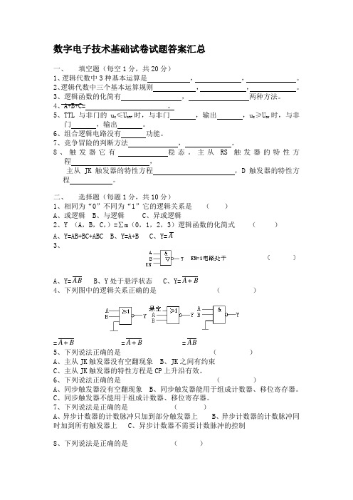
数字电子技术基础试卷试题答案汇总一、 填空题(每空1分,共20分) 1、逻辑代数中3种基本运算是 , , 。
2、逻辑代数中三个基本运算规则 , , 。
3、逻辑函数的化简有 , 两种方法。
4、A+B+C= 。
5、TTL 与非门的u I ≤U OFF 时,与非门 ,输出 ,u I ≥U ON 时,与非门 ,输出 。
6、组合逻辑电路没有 功能。
7、竞争冒险的判断方法 , 。
8、触发器它有 稳态。
主从RS 触发器的特性方程 ,主从JK 触发器的特性方程 ,D 触发器的特性方程 。
二、 选择题(每题1分,共10分)1、相同为“0”不同为“1”它的逻辑关系是 ( ) A 、或逻辑 B 、与逻辑 C 、异或逻辑2、Y (A ,B ,C ,)=∑m (0,1,2,3)逻辑函数的化简式 ( ) A 、Y=AB+BC+ABC B 、Y=A+B C 、Y=A3、A 、Y=AB B 、Y 处于悬浮状态C 、Y=B A +4、下列图中的逻辑关系正确的是 ( )=B A + =B A + =AB5、下列说法正确的是 ( ) A 、主从JK 触发器没有空翻现象 B 、JK 之间有约束 C 、主从JK 触发器的特性方程是CP 上升沿有效。
6、下列说法正确的是 ( )A 、同步触发器没有空翻现象B 、同步触发器能用于组成计数器、移位寄存器。
C 、同步触发器不能用于组成计数器、移位寄存器。
7、下列说法是正确的是 ( ) A 、异步计数器的计数脉冲只加到部分触发器上 B 、异步计数器的计数脉冲同时加到所有触发器上 C 、异步计数器不需要计数脉冲的控制8、下列说法是正确的是 ( )A、施密特触发器的回差电压ΔU=UT+-UT-B、施密特触发器的回差电压越大,电路的抗干扰能力越弱 C、施密特触发器的回差电压越小,电路的抗干扰能力越强9、下列说法正确的是()A、多谐振荡器有两个稳态B、多谐振荡器有一个稳态和一个暂稳态C、多谐振荡器有两个暂稳态10、下列说法正确的是()A、555定时器在工作时清零端应接高电平B、555定时器在工作时清零端应接低电平C、555定时器没有清零端三、判断题(每题1分,共10分)1、A+AB=A+B ()2、当输入9个信号时,需要3位的二进制代码输出。

电子信息、通信、电类专业将会遇到的面试题大全!精!!!看了让人大吃一惊.模拟电路1、基尔霍夫定理的内容是什么?(仕兰微电子)基尔霍夫电流定律是一个电荷守恒定律,即在一个电路中流入一个节点的电荷与流出同一个节点的电荷相等.基尔霍夫电压定律是一个能量守恒定律,即在一个回路中回路电压之和为零.2、平板电容公式(C=εS/4πkd)。
(未知)3、最基本的如三极管曲线特性。
(未知)4、描述反馈电路的概念,列举他们的应用。
(仕兰微电子)5、负反馈种类(电压并联反馈,电流串联反馈,电压串联反馈和电流并联反馈);负反馈的优点(降低放大器的增益灵敏度,改变输入电阻和输出电阻,改善放大器的线性和非线性失真,有效地扩展放大器的通频带,自动调节作用)(未知)6、放大电路的频率补偿的目的是什么,有哪些方法?(仕兰微电子)7、频率响应,如:怎么才算是稳定的,如何改变频响曲线的几个方法。
(未知)8、给出一个差分运放,如何相位补偿,并画补偿后的波特图。
(凹凸)9、基本放大电路种类(电压放大器,电流放大器,互导放大器和互阻放大器),优缺点,特别是广泛采用差分结构的原因。
(未知)10、给出一差分电路,告诉其输出电压Y+和Y-,求共模分量和差模分量。
(未知)11、画差放的两个输入管。
(凹凸)12、画出由运放构成加法、减法、微分、积分运算的电路原理图。
并画出一个晶体管级的运放电路。
(仕兰微电子)13、用运算放大器组成一个10倍的放大器。
(未知)14、给出一个简单电路,让你分析输出电压的特性(就是个积分电路),并求输出端某点的rise/fall时间。
(Infineon笔试试题)15、电阻R和电容C串联,输入电压为R和C之间的电压,输出电压分别为C上电压和R上电压,要求制这两种电路输入电压的频谱,判断这两种电路何为高通滤波器,何为低通滤波器。
当RC<< period - setup ? hold16、时钟周期为T,触发器D1的建立时间最大为T1max,最小为T1min。
EE笔试/面试题目集合分类--IC设计基础1、我们公司的产品是集成电路,请描述一下你对集成电路的认识,列举一些与集成电路相关的内容(如讲清楚模拟、数字、双极型、CMOS、MCU、RISC、CISC、DSP、ASIC、FPGA等的概念)。
(仕兰微面试题目)2、FPGA和ASIC的概念,他们的区别。
(未知)答案:FPGA是可编程ASIC。
ASIC:专用集成电路,它是面向专门用途的电路,专门为一个用户设计和制造的。
根据一个用户的特定要求,能以低研制成本,短、交货周期供货的全定制,半定制集成电路。
与门阵列等其它ASIC(Application Specific IC)相比,它们又具有设计开发周期短、设计制造成本低、开发工具先进、标准产品无需测试、质量稳定以及可实时在线检验等优点模拟电路1、基尔霍夫定理的内容是什么?(仕兰微电子)2、平板电容公式(C=εS/4πkd)。
(未知)3、最基本的如三极管曲线特性。
(未知)4、描述反馈电路的概念,列举他们的应用。
(仕兰微电子)5、负反馈种类(电压并联反馈,电流串联反馈,电压串联反馈和电流并联反馈);负反馈馈的优点(降低放大器的增益灵敏度,改变输入电阻和输出电阻,改善放大器的线性和非线性失真,有效地扩展放大器的通频带,自动调节作用)(未知)6、放大电路的频率补偿的目的是什么,有哪些方法?(仕兰微电子)7、频率响应,如:怎么才算是稳定的,如何改变频响曲线的几个方法。
(未知)8、给出一个查分运放,如何相位补偿,并画补偿后的波特图。
(凹凸)9、基本放大电路种类(电压放大器,电流放大器,互导放大器和互阻放大器),优缺点,特别是广泛采用差分结构的原因。
(未知)10、给出一差分电路,告诉其输出电压Y+和Y-,求共模分量和差模分量。
(未知)11、画差放的两个输入管。
(凹凸)12、画出由运放构成加法、减法、微分、积分运算的电路原理图。
并画出一个晶体管级的运放电路。
(仕兰微电子)13、用运算放大器组成一个10倍的放大器。
电子工程师面试时经常被问问题大总结时间:2011-02-15 3165次阅读【网友评论0条我要评论】收藏电源网讯以下是电源网小编多方搜集整理的电子工程师在面试时经常被面试官问到的问题,希望对各位即将找工作的工程师有所帮助。
模拟电路1、基尔霍夫定理的内容是什么?(仕兰微电子)基尔霍夫电流定律是一个电荷守恒定律,即在一个电路中流入一个节点的电荷与流出同一个节点的电荷相等. 基尔霍夫电压定律是一个能量守恒定律,即在一个回路中回路电压之和为零.2、平板电容公式(C=εS/4πkd)。
(未知)3、最基本的如三极管曲线特性。
(未知)4、描述反馈电路的概念,列举他们的应用。
(仕兰微电子)5、负反馈种类(电压并联反馈,电流串联反馈,电压串联反馈和电流并联反馈);负反馈的优点(降低放大器的增益灵敏度,改变输入电阻和输出电阻,改善放大器的线性和非线性失真,有效地扩展放大器的通频带,自动调节作用)(未知)6、放大电路的频率补偿的目的是什么,有哪些方法?(仕兰微电子)7、频率响应,如:怎么才算是稳定的,如何改变频响曲线的几个方法。
(未知)8、给出一个查分运放,如何相位补偿,并画补偿后的波特图。
(凹凸)9、基本放大电路种类(电压放大器,电流放大器,互导放大器和互阻放大器),优缺点,特别是广泛采用差分结构的原因。
(未知)10、给出一差分电路,告诉其输出电压Y+和Y-,求共模分量和差模分量。
(未知)11、画差放的两个输入管。
(凹凸)12、画出由运放构成加法、减法、微分、积分运算的电路原理图。
并画出一个晶体管级的运放电路。
(仕兰微电子)13、用运算放大器组成一个10倍的放大器。
(未知)14、给出一个简单电路,让你分析输出电压的特性(就是个积分电路),并求输出端某点的rise/fall时间。
(Infineon笔试试题)15、电阻R和电容C串联,输入电压为R和C之间的电压,输出电压分别为C上电压和R上电压,要求制这两种电路输入电压的频谱,判断这两种电路何为高通滤波器,何为低通滤波器。
ADC0803/0804 CMOS 8-bit A/D convertersLarge values of source resistance where an input bypass capacitoris not used will not cause errors as the input currents settle out priorto the comparison time. If a low pass filter is required in the system,use a low valued series resistor (< 1 kΩ) for a passive RC section oradd an op amp active filter (low pass). For applications with sourceresistances at or below 1 kΩ, a 0.1 µF bypass capacitor at the inputswill prevent pickup due to series lead inductance or a long wire. A100 Ω series resistor can be used to isolate this capacitor (both theresistor and capacitor should be placed out of the feedback loop)from the output of the op amp, if used.Analog Differential Voltage Inputs andCommon-Mode RejectionThese A/D converters have additional flexibility due to the analogdifferential voltage input. The V IN(–) input (Pin 7) can be used tosubtract a fixed voltage from the input reading (tare correction). Thisis also useful in a 4/20 mA current loop conversion. Common-modenoise can also be reduced by the use of the differential input.The time interval between sampling V IN(+) and V IN(–) is 4.5 clockperiods. The maximum error due to this time difference is given by:V(max) = (V P)(2f CM)(4.5/f CLK),where:V = error voltage due to sampling delayV P = peak value of common-mode voltagef CM = common mode frequencyFor example, with a 60 Hz common-mode frequency, f cm, and a1 MHz A/D clock, f CLK, keeping this error to 1/4 LSB (about 5 mV)would allow a common-mode voltage, V P, which is given by:V P +[V(max)(fCLK)(2fCM)(4.5)orV P +(5x10*3)(104)(6.28)(60)(4.5)+2.95VThe allowed range of analog input voltages usually places more severe restrictions on input common-mode voltage levels than this, however.An analog input span less than the full 5 V capability of the device, together with a relatively large zero offset, can be easily handled by use of the differential input. (See Reference Voltage Span Adjust). Noise and Stray PickupThe leads of the analog inputs (Pins 6 and 7) should be kept as short as possible to minimize input noise coupling and stray signal pick-up. Both EMI and undesired digital signal coupling to these inputs can cause system errors. The source resistance for these inputs should generally be below 5 kΩ to help avoid undesired noise pickup. Input bypass capacitors at the analog inputs can create errors as described previously. Full scale adjustment with any input bypass capacitors in place will eliminate these errors. Reference VoltageFor application flexibility, these A/D converters have been designed to accommodate fixed reference voltages of 5V to Pin 20 or 2.5 V to Pin 9, or an adjusted reference voltage at Pin 9. The reference can be set by forcing it at V REF/2 input, or can be determined by the supply voltage (Pin 20). Figure 6 indicates how this is accomplished.Reference Voltage Span AdjustNote that the Pin 9 (V REF/2) voltage is either 1/2 the voltage applied to the V CC supply pin, or is equal to the voltage which is externally forced at the V REF/2 pin. In addition to allowing for flexible references and full span voltages, this also allows for a ratiometric voltage reference. The internal gain of the V REF/2 input is 2, making the full-scale differential input voltage twice the voltage at Pin 9.For example, a dynamic voltage range of the analog input voltage that extends from 0 to 4 V gives a span of 4 V (4–0), so the V REF/2 voltage can be made equal to 2 V (half of the 4 V span) and full scale output would correspond to 4 V at the input.On the other hand, if the dynamic input voltage had a range of0.5 to 3.5 V, the span or dynamic input range is 3 V (3.5–0.5). To encode this 3 V span with 0.5 V yielding a code of zero, the minimum expected input (0.5 V, in this case) is applied to the V IN(–) pin to account for the offset, and the V REF/2 pin is set to 1/2 the 3 V span, or 1.5 V. The A/D converter will now encode the V IN(+) signal between 0.5 and 3.5 V with 0.5 V at the input corresponding to a code of zero and 3.5 V at the input producing a full scale output code. The full 8 bits of resolution are thus applied over this reduced input voltage range. The required connections are shown inFigure 7.Operating ModeThese converters can be operated in two modes:1) absolute mode2) ratiometric modeIn absolute mode applications, both the initial accuracy and the temperature stability of the reference voltage are important factors in the accuracy of the conversion. For V REF/2 voltages of 2.5 V, initial errors of ±10 mV will cause conversion errors of ±1 LSB due to the gain of 2 at the V REF/2 input. In reduced span applications, the initial value and stability of the V REF/2 input voltage become even more important as the same error is a larger percentage of the V REF/2 nominal value. See Figure 8.In ratiometric converter applications, the magnitude of the reference voltage is a factor in both the output of the source transducer and the output of the A/D converter, and, therefore, cancels out in the final digital code. See Figure 9.Generally, the reference voltage will require an initial adjustment. Errors due to an improper reference voltage value appear asfull-scale errors in the A/D transfer function.ERRORS AND INPUT SPAN ADJUSTMENTSThere are many sources of error in any data converter, some of which can be adjusted out. Inherent errors, such as relative accuracy, cannot be eliminated, but such errors as full-scale and zero scale offset errors can be eliminated quite easily. See Figure 7. Zero Scale ErrorZero scale error of an A/D is the difference of potential between the ideal 1/2 LSB value (9.8 mV for V REF/2=2.500 V) and that input voltage which just causes an output transition from code 0000 0000 to a code of 0000 0001.If the minimum input value is not ground potential, a zero offset can be made. The converter can be made to output a digital code of 0000 0000 for the minimum expected input voltage by biasing theV IN(–) input to that minimum value expected at the V IN(–) input to that minimum value expected at the V IN(+) input. This uses the differential mode of the converter. Any offset adjustment should be done prior to full scale adjustment.CMOS 8-bit A/D convertersADC0803/0804 SO20:plastic small outline package; 20 leads; body width 7.5 mm SOT163-1CMOS 8-bit A/D convertersADC0803/0804 DIP20:plastic dual in-line package; 20 leads (300 mil)SOT146-1ADC0803/0804 CMOS 8-bit A/D convertersDefinitionsShort-form specification — The data in a short-form specification is extracted from a full data sheet with the same type number and title. For detailed information see the relevant data sheet or data handbook.Limiting values definition — Limiting values given are in accordance with the Absolute Maximum Rating System (IEC 60134). Stress above one or more of the limiting values may cause permanent damage to the device. These are stress ratings only and operation of the device at these or at any other conditions above those given in the Characteristics sections of the specification is not implied. Exposure to limiting values for extended periods may affect device reliability.Application information — Applications that are described herein for any of these products are for illustrative purposes only. Philips Semiconductors make no representation or warranty that such applications will be suitable for the specified use without further testing or modification.DisclaimersLife support — These products are not designed for use in life support appliances, devices, or systems where malfunction of these products can reasonably be expected to result in personal injury. Philips Semiconductors customers using or selling these products for use in such applications do so at their own risk and agree to fully indemnify Philips Semiconductors for any damages resulting from such application.Right to make changes — Philips Semiconductors reserves the right to make changes in the products—including circuits, standard cells, and/or software—described or contained herein in order to improve design and/or performance. When the product is in full production (status ‘Production’), relevant changes will be communicated via a Customer Product/Process Change Notification (CPCN). Philips Semiconductors assumes no responsibility or liability for the use of any of these products, conveys no license or title under any patent, copyright, or mask work right to these products, and makes no representations or warranties that these products are free from patent, copyright, or mask work right infringement, unless otherwise specified.Contact informationFor additional information please visit.Fax: +31 40 27 24825For sales offices addresses send e-mail to:© Koninklijke Philips Electronics N.V. 2002All rights reserved. Printed in U.S.A.Date of release: 10-02Document order number:9397 750 10538。
eda技术实用教程-veriloghdl答案【篇一:eda技术与vhdl程序开发基础教程课后答案】eda的英文全称是electronic design automation2.eda系统设计自动化eda阶段三个发展阶段3. eda技术的应用可概括为4.目前比较流行的主流厂家的eda软件有、5.常用的设计输入方式有原理图输入、文本输入、状态机输入6.常用的硬件描述语言有7.逻辑综合后生成的网表文件为 edif8.布局布线主要完成9.10.常用的第三方eda工具软件有synplify/synplify pro、leonardo spectrum1.8.2选择1.eda技术发展历程的正确描述为(a)a cad-cae-edab eda-cad-caec eda-cae-cadd cae-cad-eda2.altera的第四代eda集成开发环境为(c)a modelsimb mux+plus iic quartus iid ise3.下列eda工具中,支持状态图输入方式的是(b)a quartus iib isec ispdesignexpertd syplify pro4.下列几种仿真中考虑了物理模型参数的仿真是(a)a 时序仿真b 功能仿真c 行为仿真d 逻辑仿真5.下列描述eda工程设计流程正确的是(c)a输入-综合-布线-下载-仿真b布线-仿真-下载-输入-综合c输入-综合-布线-仿真-下载d输入-仿真-综合-布线-下载6.下列编程语言中不属于硬件描述语言的是(d)a vhdlb verilogc abeld php1.8.3问答1.结合本章学习的知识,简述什么是eda技术?谈谈自己对eda技术的认识?答:eda(electronic design automation)工程是现代电子信息工程领域中一门发展迅速的新技术。
2.简要介绍eda技术的发展历程?答:现代eda技术是20世纪90年代初从计算机辅助设计、辅助制造和辅助测试等工程概念发展而来的。