FPGA可编程逻辑器件芯片XC5VFX100T-2FFG1738I中文规格书
- 格式:pdf
- 大小:378.03 KB
- 文档页数:5
IntroductionArtix®-7 FPGAs are available in -3, -2, -1, -1LI, and -2L speed grades, with -3 having the highest performance. The Artix-7FPGAs predominantly operate at a 1.0V core voltage. The -1LI and -2L devices are screened for lower maximum static power and can operate at lower core voltages for lower dynamic power than the -1 and -2 devices, respectively. The -1LI devices operate only atV CCINT =V CCBRAM =0.95V and have the same speed specifications as the -1 speed grade. The -2L devices can operate at either of two V CCINT voltages, 0.9V and 1.0V and are screened for lower maximum static power. Whenoperated at V CCINT =1.0V, the speed specification of a -2L device is the same as the -2 speed grade. When operated at V CCINT =0.9V, the -2L static and dynamic power is reduced.Artix-7 FPGA DC and AC characteristics are specified in commercial, extended, industrial, expanded (-1Q), and military (-1M) temperature ranges. Except the operating temperature range or unless otherwise noted, all the DC and AC electrical parameters are the same for a particular speed grade (that is, the timing characteristics of a -1Mspeed grade military device are the same as for a -1C speed grade commercial device). However, only selected speed grades and/or devices are available in each temperature range. For example, -1M is only available in thedefense-grade Artix-7Q family and -1Q is only available in XA Artix-7FPGAs.All supply voltage and junction temperature specifications are representative of worst-case conditions. The parameters included are common to popular designs and typical applications.Available device and package combinations can be found in :•7Series FPGAs Overview (DS180)•Defense-Grade 7Series FPGAs Overview (DS185)•XA Artix-7 FPGAs Overview (DS197)DC CharacteristicsTable 1:Absolute Maximum Ratings (1)SymbolDescription Min Max UnitsFPGA Logic V CCINT Internal supply voltage –0.5 1.1V V CCAUX Auxiliary supply voltage–0.5 2.0V V CCBRAM Supply voltage for the block RAM memories –0.5 1.1V V CCO Output drivers supply voltage for HR I/O banks –0.5 3.6V V REF Input reference voltage –0.5 2.0V V IN (2)(3)(4)I/O input voltage–0.4V CCO +0.55V I/O input voltage (when V CCO =3.3V) for V REF and differential I/O standards except TMDS_33(5)–0.4 2.625V V CCBATTKey memory battery backup supply–0.52.0VGTP Transceiver V MGTAVCC Analog supply voltage for the GTP transmitter and receiver circuits–0.5 1.1V V MGTAVTT Analog supply voltage for the GTP transmitter and receiver termination circuits –0.5 1.32V V MGTREFCLK Reference clock absolute input voltage–0.5 1.32V V INReceiver (RXP/RXN) and Transmitter (TXP/TXN) absolute input voltage–0.51.26V找FPGA ,上赛灵思半导体(深圳)有限公司I DCIN-FLOAT DC input current for receiver input pins DC coupled RX termination =floating –14mA I DCIN-MGTAVTT DC input current for receiver input pins DC coupled RX termination =V MGTAVTT –12mA I DCIN-GND DC input current for receiver input pins DC coupled RX termination =GND – 6.5mA I DCOUT-FLOAT DC output current for transmitter pins DC coupled RX termination =floating –14mA I DCOUT-MGTAVTTDC output current for transmitter pins DC coupled RX termination =V MGTAVTT –12mA XADC V CCADC XADC supply relative to GNDADC –0.5 2.0V V REFPXADC reference input relative to GNDADC–0.52.0VTemperature T STG Storage temperature (ambient)–65150°C T SOL Maximum soldering temperature for Pb/Sn component bodies (6)–+220°C Maximum soldering temperature for Pb-free component bodies (6)–+260°C T j Maximum junction temperature (6)–+125°CNotes:1.Stresses beyond those listed under Absolute Maximum Ratings might cause permanent damage to the device. These are stress ratings only, and functional operation of the device at these or any other conditions beyond those listed under Operating Conditions is not implied.Exposure to Absolute Maximum Ratings conditions for extended periods of time might affect device reliability.2.The lower absolute voltage specification always applies.3.For I/O operation, refer to 7Series FPGAs SelectIO Resources User Guide (UG471).4.The maximum limit applies to DC signals. For maximum undershoot and overshoot AC specifications, see Table 4.5.See Table 9 for TMDS_33 specifications.6.For soldering guidelines and thermal considerations, see 7Series FPGA Packaging and Pinout Specification (UG475).Table 2:Recommended Operating Conditions (1)(2)Symbol Description Min Typ Max UnitsFPGA LogicV CCINT (3)For -3, -2, -2LE (1.0V), -1, -1Q, -1M devices: internal supply voltage0.95 1.00 1.05V For -1LI (0.95V) devices: internal supply voltage 0.920.950.98V For -2LE (0.9V) devices: internal supply voltage 0.870.900.93V V CCAUX Auxiliary supply voltage1.71 1.80 1.89V V CCBRAM (3)For -3, -2, -2LE (1.0V), -2LE (0.9V), -1, -1Q, -1M devices: block RAM supply voltage0.95 1.00 1.05V For -1LI (0.95V) devices: block RAM supply voltage 0.920.950.98V V CCO (4)(5)Supply voltage for HR I/O banks 1.14– 3.465V V IN (6)I/O input voltage–0.20–V CCO +0.20V I/O input voltage (when V CCO =3.3V) for V REF and differential I/O standards except TMDS_33(7)–0.20– 2.625V I IN (8)Maximum current through any pin in a powered or unpowered bank when forward biasing the clamp diode.––10mA V CCBATT (9)Battery voltage1.0–1.89VGTP TransceiverV MGTAVCC (10)Analog supply voltage for the GTP transmitter and receiver circuits0.97 1.0 1.03V V MGTAVTT (10)Analog supply voltage for the GTP transmitter and receiver termination circuits1.171.21.23VXADC V CCADCXADC supply relative to GNDADC1.711.801.89VTable 1:Absolute Maximum Ratings (1) (Cont’d)Symbol DescriptionMin Max UnitsTable 3:DC Characteristics Over Recommended Operating ConditionsSymbolDescriptionMin Typ (1)Max Units V DRINT Data retention V CCINT voltage (below which configuration data might be lost)0.75––V V DRI Data retention V CCAUX voltage (below which configuration data might be lost) 1.5––V I REF V REF leakage current per pin––15µA I L Input or output leakage current per pin (sample-tested)––15µA C IN (2)Die input capacitance at the pad––8pF I RPU Pad pull-up (when selected) @ V IN =0V, V CCO =3.3V 90–330µA Pad pull-up (when selected) @ V IN =0V, V CCO =2.5V68–250µA Pad pull-up (when selected) @ V IN =0V, V CCO =1.8V 34–220µA Pad pull-up (when selected) @ V IN =0V, V CCO =1.5V 23–150µA Pad pull-up (when selected) @ V IN =0V, V CCO =1.2V12–120µA I RPD Pad pull-down (when selected) @ V IN =3.3V68–330µA I CCADC Analog supply current, analog circuits in powered up state ––25mA I BATT (3)Battery supply current––150nA R IN_TERM (4)Thevenin equivalent resistance of programmable input termination to V CCO /2 (UNTUNED_SPLIT_40)284055ΩThevenin equivalent resistance of programmable input termination to V CCO /2 (UNTUNED_SPLIT_50)355065ΩThevenin equivalent resistance of programmable input termination to V CCO /2 (UNTUNED_SPLIT_60)446083ΩDIFF_SSTL18_II0.3000.9001.4250.100–(V CCO /2)–0.600(V CCO /2)+0.60013.4–13.4Notes:1.V ICM is the input common mode voltage.2.V ID is the input differential voltage (Q –Q).3.V OL is the single-ended low-output voltage.4.V OH is the single-ended high-output voltage.Table 10:Complementary Differential SelectIO DC Input and Output Levels (Cont’d)I/O Standard V ICM (1)V ID (2)V OL (3)V OH (4)I OL I OH V, Min V,Typ V, Max V,Min V, MaxV, Max V, Min mA, Max mA, MinAC Switching CharacteristicsAll values represented in this data sheet are based on the speed specifications from the ISE® Design Suite and Vivado®Design Suite as outlined in Table12.Table 12:Artix-7 FPGA Speed Specification Version By DeviceVersion In:Typical V CCINTDeviceISE 14.7Vivado 2018.2(Table2)N/A 1.22 1.0V XC7A12T, XC7A15T, XC7A25T, XC7A35T, XC7A50T, XC7A75TN/A 1.220.95V XC7A12T, XC7A15T, XC7A25T, XC7A35T, XC7A50T, XC7A75T, XC7A100T,XC7A200TN/A 1.140.9V XC7A12T, XC7A15T, XC7A25T, XC7A35T, XC7A50T, XC7A75T1.10 1.22 1.0V XC7A100T, XC7A200T1.07 1.140.9V XC7A100T, XC7A200TN/A 1.15 1.0V XA7A12T, XA7A15T, XA725T, XA7A35T, XA7A50T, XA7A75T1.07 1.15 1.0V XA7A100T1.06 1.11 1.0V XQ7A100T, XQ7A200TN/A 1.11 1.0V XQ7A50T。

Chapter2 Power Distribution SystemChapter 2:Power Distribution SystemTable 2-2 lists the PCB decoupling capacitor guidelines per V CC supply rail for Artix-7devices.CSGA324XC7S5001351111123124FTGB196XC7S5001351111113124FGGA484XC7S5001351111124124FGGA484XC7S7501471111137124FGGA676XC7S7501471111137124FGGA484XC7S10001581111137124FGGA676XC7S1001581111137124Notes:1.PCB capacitor specifications are listed in Table 2-5.2.Total includes all capacitors for all supplies. The values in this table account for the number of I/O banks in the device.3.One 47µF (or 100µF) capacitor is required for up to four V CCO banks when powered by the same voltage.4.Decoupling capacitors cover down to approximately 100KHz.PackageDeviceV CCINTV CCBRAMV CCAUXV CCO (per Bank)330µF 100µF 4.7µF 0.47µF 100µF 47µF 4.7µF 0.47µF 47µF 4.7µF 0.47µF47µF or100µF (3)4.7µF 0.47µFTable 2-2:Required PCB Capacitor Quantities per Device: Artix-7Devices (1)(2)PackageDeviceV CCINTV CCBRAM V CCAUXV CCO Bank 0V CCO all other Banks(per Bank)680µF 330µF 100µF 47µF 4.7µF 0.47µF 100µF 47µF 4.7µF 0.47µF 47µF 4.7µF 0.47µF 47µF47µF or100µF (3)4.7µF 0.47µFCPG238XC7A12T 00101201011121124CSG325XC7A12T 00101201011121124CPG236XC7A15TXA7A15T 0122111121124CPG238XC7A25T 00102301011121124CSG325XC7A25T 00102301011121124CPG236XC7A35T XA7A35T 0123111121124CPG236XC7A50T XA7A50T 01003510011121124FTG256XC7A15T 00102201011231124FTG256XC7A35T 00102301011231124FTG256XC7A50T 01003510011231124FTG256XC7A75T 01004610021231124FTG256XC7A100T 01006810021231124CSG324XC7A15T XA7A15T 0122111241124CSG324XC7A35T XA7A35T 00102301011241124CSG324XC7A50T XA7A50T01003510011241124FFG1930RF1930XC7VX980T XQ7VX980T 600110201010011FLG1930XC7VX1140T 600100211010011FLG1155XC7VH580T 300100111010011FLG1931XC7VH580T 300100111010011FLG1932XC7VH870T511161111Notes:1.PCB Capacitor specifications are listed in Table 2-5.2.Total includes all capacitors for all supplies, except for the MGT supplies MGTAVCC, MGTVCCAUX, and MGTAVTT, which are covered in UG476, 7 SeriesFPGAs GTX/GTH Transceivers User Guide . The values in this table account for the number of I/O banks in the device.3.See UG471, 7 Series FPGAs SelectIO Resources User Guide for a description of the VCCAUX_IO rail specification to see which I/O banks are grouped together ineach VCCAUX_IO group. See UG475, 7 Series FPGAs Packaging and Pinout Product Specification to see which I/O banks are grouped together in each VCCAUX_IO group.4.One 47µF (or 100µF) capacitor is required for up to four V CCO banks when powered by the same voltage.5.Decoupling capacitors cover down to approximately 100KHz.PackageDeviceV CCINT V CCBRAM V CCAUXV CCAUX_IO per Group (3)V CCO Bank 0V CCO all otherBanks (per Bank)680µF330µF 4.7µF 660µF 330µF 100µF 4.7µF 47µF 4.7µF 100µF 47µF 4.7µF 47µF 47µF or 100µF (4)Chapter 2:Power Distribution SystemTable 2-6 lists the capacitors present in the packages for Kintex-7devices.0.47µFC >0.47µF 06032-Terminal Ceramic X7R or X5R0.5nH1m Ω<ESR <20m Ω6.3VGRM188R70J474KA01Notes:1.Values can be larger than specified.2.Body size can be smaller than specified.3.ESR must be within the specified range.4.Voltage rating can be higher than specified.Table 2-5:PCB Capacitor Specifications (Continued)Ideal Value Value Range (1)Body Size (2)Type ESL Maximum ESR Range (3)Voltage Rating (4)Suggested Part Number Table 2-6:Package Capacitor Quantities per Device: Kintex-7Devices (1)Package DeviceV CCINT V CCAUX V CCAUX_IO per Group (2)V CCO per Bank (3)2.2μF 2.2μF 1.0μF 0.47μF FBG484FBV484XC7K70T 21N/A 1FBG484FBV484XC7K160T 21N/A 1FBG676FBV676XC7K70T 21N/A 1FBG676FBV676XC7K160T 21N/A 1FBG676FBV676XC7K325T 2111FBG676FBV676XC7K410T 2111FBG900FBV900XC7K325T 2111FBG900FBV900XC7K410T 2111FFG676FFV676XC7K160T XA7K160T 4211FFG676FFV676RF676XC7K325T XQ7K325T 4211FFG676FFV676RF676XC7K410T XQ7K410T4211。
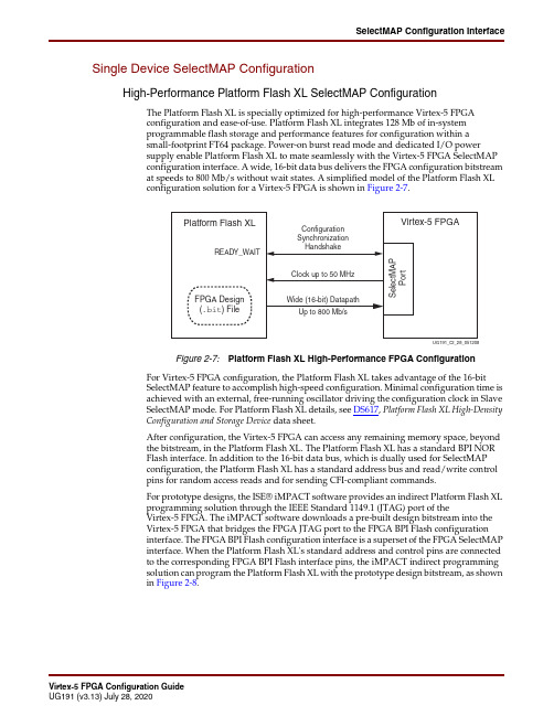
SelectMAP Configuration InterfaceSingle Device SelectMAP ConfigurationHigh-Performance Platform Flash XL SelectMAP ConfigurationThe Platform Flash XL is specially optimized for high-performance Virtex-5 FPGAconfiguration and ease-of-use. Platform Flash XL integrates 128Mb of in-systemprogrammable flash storage and performance features for configuration within asmall-footprint FT64 package. Power-on burst read mode and dedicated I/O powersupply enable Platform Flash XL to mate seamlessly with the Virtex-5 FPGA SelectMAPconfiguration interface. A wide, 16-bit data bus delivers the FPGA configuration bitstreamat speeds to 800Mb/s without wait states. A simplified model of the Platform Flash XLconfiguration solution for a Virtex-5 FPGA is shown in Figure2-7.UG191_c2_28_051208Figure 2-7:Platform Flash XL High-Performance FPGA Configuration For Virtex-5 FPGA configuration, the Platform Flash XL takes advantage of the 16-bitSelectMAP feature to accomplish high-speed configuration. Minimal configuration time isachieved with an external, free-running oscillator driving the configuration clock in SlaveSelectMAP mode. For Platform Flash XL details, see DS617, Platform Flash XL High-DensityConfiguration and Storage Device data sheet.After configuration, the Virtex-5 FPGA can access any remaining memory space, beyondthe bitstream, in the Platform Flash XL. The Platform Flash XL has a standard BPI NORFlash interface. In addition to the 16-bit data bus, which is dually used for SelectMAPconfiguration, the Platform Flash XL has a standard address bus and read/write controlpins for random access reads and for sending CFI-compliant commands.For prototype designs, the ISE® iMPACT software provides an indirect Platform Flash XLprogramming solution through the IEEE Standard 1149.1 (JTAG) port of theVirtex-5FPGA. The iMPACT software downloads a pre-built design bitstream into theVirtex-5FPGA that bridges the FPGA JTAG port to the FPGA BPI Flash configurationinterface. The FPGA BPI Flash configuration interface is a superset of the FPGA SelectMAPinterface. When the Platform Flash XL's standard address and control pins are connectedto the corresponding FPGA BPI Flash interface pins, the iMPACT indirect programmingsolution can program the Platform Flash XL with the prototype design bitstream, as shownin Figure2-8.Chapter 2:Configuration InterfacesFigure 2-23 shows the BPI-Up configuration waveforms.Notes related to Figure 2-23:∙CCLK is output in BPI modes. The BPI Flash does not require CCLK, but the Virtex-5FPGA uses the rising edge of CCLK to sample D[max:0] pins.∙The Virtex-5 FPGA stops loading the bitstream after the DONE pin goes High.∙Dual-mode configuration I/O switches to User mode after the GTS_cycle. By default,this is one cycle after DONE goes High.∙M can be 7 or 15.∙FCS_B, FOE_B, and FWE_B should have weak pull-ups after configuration through either I/O constraints or external pull-up resistors.∙The first address 0 for BPI-Up is extended for multiple cycles due to the initial latency.RS[1:0]Output Dual Revision Select pins. Not used for typical single bitstream applications.RS[1:0] are 3-stated and pulled up with weak resistors during the initialconfiguration if the HSWAP pin enables the pull ups. If pull ups aredisabled, then a weak external pull up is required (after power-up orassertion of PROGRAM_B). RS[1:0] are actively driven Low to load thefallback bitstream when a configuration error is detected. RS[1:0] canalso be controlled by the user through the bitstream or ICAP. See “Fallback MultiBoot,” page 153.CSO_B Output Dual Parallel daisy chain active-Low chip select output. Not used in singleFPGA applications.Table 2-9:Virtex-5 Device BPI Configuration Interface Pins (Continued)Pin NameTypeDedicated or Dual-PurposeDescriptionFigure 2-23:Virtex-5 Device BPI-Up Configuration WaveformsCCLKINIT_BFC S _BFOE_BFWE_BADDR[25:0]D[M:0]DONEUG191_c2_26_011708Byte Peripheral Interface Parallel Flash ModePower-On Sequence PrecautionsAt power-on, the FPGA automatically starts its configuration procedure. When the FPGAis in a Master-BPI configuration mode, the FPGA asserts FCS_B Low and drives a sequenceof addresses to read the bitstream from a BPI Flash. The BPI Flash must be ready forasynchronous reads before the FPGA drives FCS_B Low and outputs the first address toensure the BPI Flash can output the stored bitstream.Because different power rails can supply the FPGA and BPI Flash or because the FPGA andBPI flash can respond at different times along the ramp of a shared power supply, specialattention to the FPGA and BPI Flash power-on sequence or power-on ramps is essential.The power-on sequence or power supply ramps can cause the FPGA to awake before theBPI Flash or vice versa. For many systems with near-simultaneous power supply ramps,the FPGA power-on reset time (TPOR) can sufficiently delay the start of the FPGAconfiguration procedure such that the BPI Flash becomes ready before the start of theFPGA configuration procedure. In general, the system design must consider the effect ofthe power sequence, the power ramps, FPGA power-on reset time, and BPI Flashpower-on reset time on the timing relation between the start of FPGA configuration andthe readiness of the BPI Flash for asynchronous reads. Check DS202, Virtex-5 FPGA DataSheet: DC and Switching Characteristics data sheet for Virtex-5 FPGA power supplyrequirements and timing. Check DS617, Platform Flash XL High-Density Configuration andStorage Device data sheet for the BPI Flash power supply requirements and timing.One of the following system design approaches can ensure that the BPI Flash is ready forasynchronous reads before the FPGA starts its configuration procedure:∙Control the sequence of the power supplies such that the BPI Flash is certain to be powered and ready for asynchronous reads before the FPGA begins its configurationprocedure.∙Hold the FPGA PROGRAM_B pin Low from power-up to delay the start of the FPGA configuration procedure and release the PROGRAM_B pin to High after the BPI flashis fully powered and is able to perform asynchronous reads.∙Hold the FPGA INIT_B pin Low from power-up to delay the start of the FPGA configuration procedure and release the INIT_B pin to High after the BPI flashbecomes ready for asynchronous reads.See the Power-On Precautions if 3.3V Supply is Last in Sequence subsection of the Master BPIMode section in UG332, Spartan-3 Generation Configuration User Guide, for reference. Page Mode SupportMany NOR Flash devices support asynchronous page reads. The first access to a pageusually takes the longest time (~100ns), subsequent accesses to the same page take lesstime (~25ns). The following parameters are bitstream programmable in Virtex-5 devices totake advantage of page reads and maximize the CCLK frequency:∙Page sizes of 1 (default), 4, or 8.If the actual Flash page size is larger then 8, the value of 8 should be used to maximizethe efficiency.∙First access CCLK cycles of 1 (default), 2, 3, or 4. CCLK cycles must be 1 if the page size is 1.∙CCLK frequencyThe sequence of page-mode operation is controlled by the Virtex-5 bitstream (seeTable6-15). After an FPGA reset, the default page size is 1, the first access CCLK is 1, andChapter 2:Configuration InterfacesBoard Layout for Configuration Clock (CCLK)。

Chapter 1:Packaging OverviewPin DefinitionsTable1-12 lists the pin definitions used in 7series FPGAs packages.Note:There are dedicated general purpose user I/O pins listed separately in Table1-12. There are also multi-function pins where the pin names start with either IO_LXXY_ZZZ_# or IO_XX_ZZZ_#,where ZZZ represents one or more functions in addition to being general purpose user I/O. If notused for their special function, these pins can be user I/O.user I/O after stage 2 configuration is complete.Table 1-12:7Series FPGAs Pin DefinitionsPin Name Type Direction DescriptionUser I/O PinsIO_LXXY_# IO_XX_#Dedicated Input/OutputMost user I/O pins are capable of differential signalingand can be implemented as pairs. The top and bottom I/O pins are always single ended. Each user I/O is labeledIO_LXXY_#, where:°IO indicates a user I/O pin°L indicates a differential pair, with XX a unique pair inthe bank and Y = [P|N] for the positive/negative sidesof the differential pair°# indicates a bank numberConfiguration PinsFor more information, see the Configuration Pin Definitions table in UG470, 7Series FPGAs Configuration User Guide.CCLK_0Dedicated(1)Input/Output Configuration clock. Output in Master mode or input in Slave modeDONE_0Dedicated(1)Bidirectional DONE indicates successful completion of configuration(active High)INIT_B_0Dedicated(1)Bidirectional(open-drain)Indicates initialization of configuration memory (active Low)M0_0, M1_0, or M2_0Dedicated(1)Input Configuration mode selectionPROGRAM_B_0Dedicated(1)Input Asynchronous reset to configuration logic (active Low) TCK_0Dedicated(1)Input JTAG clockTDI_0Dedicated(1)Input JTAG data inputTDO_0Dedicated(1)Output JTAG data outputTMS_0Dedicated(1)Input JTAG mode selectChapter 2:7Series FPGAs Package FilesTo download all available Artix-7 FPGAs package/device/pinout files click here: Table 2-2:Artix-7 FPGAs Package/Device Pinout FilesChapter 3:Device DiagramsArtix-7 FPGAs Device DiagramsDeviceCP236CPG236CPG238CS324CSG324CS325CSG325FT256FTG256SB484SBG484SBV484RS484FG484FGG484FG676FGG676FB484FBG484RB484FB676FBG676RB676FF1156FFG1156XC7A12T page 100page 105XC7A15T page 98page 102page 109page 111page 113XC7A25T page 100page 107XC7A35T page 98page 102page 109page 111page 113XC7A50T page 98page 102page 109page 111page 113XC7A75T page 102page 111page 116page 119XC7A100T page 102page 111page 116page 119XC7A200T page 122page 125page 128page 131XA7A12T page 100page 105XA7A15T page 98page 102page 109page 113XA7A25T page 100page 107XA7A35T page 98page 102page 109XA7A50T page 98page 102page 109XA7A75T page 102page 116XA7A100Tpage 102page 116Table 5-1:Thermal Resistance Data—All DevicesPackage PackageBody Size DevicesθJB(°C/W)θJA(°C/W)θJC(°C/W)θJA-Effective (°C/W)(1)@250 LFM@500 LFM@750 LFMSpartan-7 FPGAsCPGA1968 x 8XC7S615.135.08.4630.128.627.9 CPGA1968 x 8XA7S615.135.08.4630.128.627.9 CPGA1968 x 8XC7S1515.135.08.4630.128.627.9 CPGA1968 x 8XA7S1515.135.08.4630.128.627.9 CSGA22513 x 13XC7S617.432.210.626.725.124.2 CSGA22513 x 13XA7S617.432.210.626.725.124.2 CSGA22513 x 13XC7S1517.432.210.626.725.124.2 CSGA22513 x 13XA7S1517.432.210.626.725.124.2 CSGA22513 x 13XC7S2515.630.69.427.123.524.4 CSGA22513 x 13XA7S2515.630.69.427.123.524.4 CSGA32415 x 15XC7S259.422.1 5.6518.116.716.2 CSGA32415 x 15XA7S259.422.1 5.6518.116.716.2 CSGA32415 x 15XC7S507.620.1 4.4715.914.814.1 CSGA32415 x 15XA7S507.620.1 4.4715.914.814.1 FTGB19615 x 15XC7S613.727.88.922.521.120.0 FTGB19615 x 15XC7S1513.727.88.922.521.120.0 FTGB19615 x 15XC7S2512.526.27.120.919.418.6 FTGB19615 x 15XC7S508.822.6 5.317.315.915.1 FGGA48423 x 23XC7S509.217.9 5.8513.812.712.1 FGGA48423 x 23XA7S509.217.9 5.8513.812.712.1 FGGA48423 x 23XC7S75 6.815.8 3.8512.111.010.4 FGGA48423 x 23XA7S75 6.815.8 3.8512.111.010.4 FGGA48423 x 23XC7S100 6.815.8 3.8512.111.010.4 FGGA48423 x 23XA7S100 6.815.8 3.8512.111.010.4 FGGA67627 x 27XC7S75 6.815.0 3.7111.210.29.7 FGGA67627 x 27XA7S75 6.815.0 3.7111.210.29.7 FGGA67627 x 27XC7S100 6.815.0 3.7111.210.29.7 FGGA67627 x 27XA7S100 6.815.0 3.7111.210.29.7 Artix-7 FPGAsCP/CPG23610 x 10XC7A15T7.924.8 5.2920.318.918.0 CPG23610 x 10XA7A15T7.924.8 5.2920.318.918.0 CP/CPG23610 x 10XC7A35T7.924.8 5.2920.318.918.0。
Master BPI Configuration InterfaceDetermining the Maximum Configuration Clock FrequencyIn Master BPI mode, the FPGA delivers the configuration clock. The master configuration clock frequency of the FPGA is set through the BitGen -g ConfigRate option. The BitGen -g ConfigRate option sets the nominal configuration clock frequency. The default BitGen ConfigRate setting of 2 is recommended. This default value sets thenominal master CCLK frequency to 2MHz, which satisfies timing requirements for the leading BPI flash families. If the timing requirements discussed in this section are satisfied, the BitGen ConfigRate setting can be increased for a faster configuration time. When determining a valid ConfigRate setting, these timing parameters must be considered:•FPGA nominal master CCLK frequency (BitGen ConfigRate)•FPGA Master CCLK frequency tolerance (FMCCKTOL)•A[25:0] outputs valid after CCLK falling edge (TBPICCO)•BPI flash address to output valid (access) time (TACC)•FPGA data setup time to CCLK rising edge (TBPIDCC)The master configuration clock of the FPGA has a tolerance of FMCCKTOL. Due to the master configuration clock tolerance (FMCCKTOL), the BitGen -g ConfigRate option must be checked so that half the period for the worst-case (fastest) master CCLK frequency is greater than the sum of the FPGA address valid time, BPI flash access time, and FPGA set up time, as shown in Equation 2-1.Equation 2-1Power-On Sequence PrecautionsAt power-on, the FPGA automatically starts its configuration procedure. When the FPGA is in a Master-BPI configuration mode, the FPGA asserts FCS_B Low and drives a sequence of addresses to read the bitstream from a parallel NOR flash. The parallel NOR flash must be ready for asynchronous reads before the FPGA drives FCS_B Low and outputs the first address to ensure the parallel NOR flash can output the stored bitstream.Because different power rails can supply the FPGA and parallel NOR flash or because the FPGA and parallel NOR flash can respond at different times along the ramp of a shared power supply, special attention to the FPGA and parallel NOR flash power-on sequence or power-on ramps is essential. The power-on sequence or power supply ramps can cause the FPGA to awake before the parallel NOR flash or vice versa. For many systems with near-simultaneous power supply ramps, the FPGA power-on reset time (T POR ) can sufficiently delay the start of the FPGA configuration procedure such that the parallel NOR flash becomes ready before the start of the FPGA configuration procedure. In general, the system design must consider the effect of the power sequence, the power ramps, FPGA power-on reset time, and parallel NOR flash power-on reset time on the timing relation between the start of FPGA configuration and the readiness of the parallel NOR flash for asynchronous reads. Check DS162, Spartan-6 FPGA Data Sheet: DC and Switching Characteristics , for Spartan-6 FPGA power supply requirements and timing.One of the following system design approaches can ensure that the parallel NOR flash is ready for asynchronous reads before the FPGA starts its configuration procedure:•Control the sequence of the power supplies such that the parallel NOR flash is certainto be powered and ready for asynchronous reads before the FPGA begins itsconfiguration procedure.12ConfigRate ×FMCCKTOLMAX×------------------------------------------------------------------------------------------------TBPICCO TACC TBPIDCC ++≥Chapter 2:Configuration Interface Basics•Hold the FPGA PROGRAM_B pin Low from power-up to delay the start of the FPGAconfiguration procedure and release the PROGRAM_B pin to High after the parallel NOR flash is fully powered and is able to perform asynchronous reads.•Hold the FPGA INIT_B pin Low from power-up to delay the start of the FPGA configuration procedure and release the INIT_B pin to High after the parallel NOR flash becomes ready for asynchronous reads.External Configuration Clock for Master ModesBy default, Spartan-6 FPGAs perform master mode configuration using an internally generated clock source. However, Spartan-6 FPGAs support the ability to dynamically switch to an external clock source during master mode configuration. The external clock source is effective for an application where faster and stable configuration times are needed.USERCCLK is a dual-purpose pin that can be used by the application as GCLK0 after the configuration. To enable the external clock source during master mode configuration, the ExtMasterCclk_en option in BitGen must be enabled. The USERCCLK frequency can be divided down using the ExtMasterCclk_divide BitGen option. The allowable values are 1 (default) and all even numbers between 2 and 1022. The I/O standard for theUSERCCLK is LVCMOS 8mA slow slew rate. The configuration begins with the CCLK generated by the FPGA internal oscillator. When the configuration clock register setting is reached in the bitstream, the FPGA switches from the internal oscillator to the clock found on USERCCLK (or divided down, as set by the BitGen option ExtMasterCclk_divide ). The clock multiplexer is designed to generate a glitchless output clock during thetransition. Care must be exercised when also using this clock output as an input to the design. When the end of startup (EOS) completes, the I/O standard for this pin as specified by the design is enabled. At this time, the input of this pin might glitch as the I/O changes from the default I/O standard to the user-specified I/O standard.Board Layout for Configuration Clock (CCLK)The Spartan-6 FPGA configuration I/Os use the LVCMOS slow slew rate 8mA I/O standard. This requires more attention to PCB trace routing and termination for proper signal integrity.These basic guidelines must be followed:•Route the CCLK net as a 50Ω controlled impedance transmission line.•Always route the CCLK net without any branching; do not use a star topology (Figure 2-25).•Stubs, if necessary, must be shorter than 8mm (0.3 inches).Table 2-8:Spartan-6 FPGA External Configuration Clock Interface Pin Pin NameType Dedicated or Dual-Purpose Description USERCCLK Input Dual-purpose Externalconfiguration clocksource for all masterconfiguration modesChapter 3:Boundary-Scan and JTAG ConfigurationChapter 4:User PrimitivesGenerating PROM FilesParallel Bus Bit OrderTraditionally, in SelectMAP x8 mode, configuration data is loaded one byte per CCLK, with the most-significant bit (MSB) of each byte presented to the D0 pin. Although this convention (D0 = MSB, D7 = LSB) differs from many other devices, it is consistent across all Xilinx FPGAs. The bit-swap rule also applies to Spartan-6 FPGA BPI x8 modes (see Bit Swapping, page 80).In Spartan-6 devices, the bit-swap rule is extended to x16 bus widths; the data is bit swapped within each byte.Table 5-8 and Table 5-9 show examples of a sync word inside a bitstream. These examples illustrate what is expected at the FPGA data pins when using parallel configuration modes, such as Slave SelectMAP and Master SelectMAP (BPI) modes.Delaying ConfigurationThere are two ways to delay configuration for Spartan-6 devices:•Hold the INIT_B pin Low during initialization. When INIT_B has gone High,configuration cannot be delayed by subsequently pulling INIT_B Low.•Hold the PROGRAM_B pin Low. The signals relating to initialization and delaying configuration are defined in Table 5-10.Table 5-8:Sync Word Bit Swap Example Sync Word[31:24](1)[23:16][15:8][7:0]Bitstream Format0xAA 0x990x550x66Bit Swapped0x550x990xAA 0x66Notes:1.[31:24] changes from 0xAA to 0x55 after bit swapping.Table 5-9:Sync Word Data Sequence Example for x8 and x16 ModesCCLK Cycle1234D[7:0] pins for x80x550x990xAA 0x66D[15:0] pins for x160x55990xAA66Table 5-10:Signals Relating to Initialization and Delaying Configuration Signal Name Type Access (1)Description PROGRAM_B Input Externally accessible via thePROGRAM_B pin.Global asynchronous chip reset. Can be held Low to delay configuration.INIT_B Input, Output, or Open DrainExternally accessible via the INIT_B pin.Before the Mode pins are sampled, INIT_B is an input thatcan be held Low to delay configuration.After the Mode pins are sampled, INIT_B is an open-drain, active-Low output that indicates whether a CRCerror occurred during configurati on or a readback CRCerror occurred after configuration (when enabled):0 = CRC error1 = No CRC error (needs an external pull-up)。

SPI InterfacesTable 43:SPI Master Mode Interface Switching Characteristics (1)Symbol DescriptionMin Typ Max Units T DCMSPICLK SPI master mode clock duty cycle –50–%T MSPIDCK Input setup time for SPI {0,1}_MISO 2.00––ns T MSPICKD Input hold time for SPI {0,1}_MISO8.20––ns T MSPICKO Output delay for SPI {0,1}_MOSI and SPI {0,1}_SS –3.10– 3.90nsT MSPISSCLK Slave select asserted to first active clock edge 1––F SPI_REF_CLK cycles T MSPICLKSS Last active clock edge to slave select deasserted 0.5––F SPI_REF_CLK cyclesF MSPICLK SPI master mode device clock frequency ––50.00MHz F SPI_REF_CLK SPI reference clock frequency––200.00MHzNotes:1.Test conditions: LVCMOS33, slow slew rate, 8mA drive strength, 15pF loads.Figure 12:SPI Master (CPHA =0) Interface Timing DiagramFigure 13:SPI Master (CPHA =1) Interface Timing DiagramPL Performance CharacteristicsThis section provides the performance characteristics of some common functions and designs implemented in the PL. The numbers reported here are worst-case values; they have all been fully characterized. These values are subject to the same guidelines as the AC Switching Characteristics, page 15. In each table, the I/O bank type is either High Performance (HP) or High Range (HR).Table 53 provides the maximum data rates for applicable memory standards using the Zynq-7000SoC memory PHY. The final performance of the memory interface is determined through a complete design implemented in the Vivado or ISE Design Suite, following guidelines in the Zynq-7000 SoC and 7Series Devices Memory Interface Solutions User Guide (UG586).Table 52:PL Networking Applications Interface PerformancesDescriptionI/O Bank Type Speed GradeUnits -3E -2E/-2I/-2LI-1C/-1I -1Q/-1LQ SDR LVDS transmitter (using OSERDES; DATA_WIDTH =4 to 8)HR 710710625625Mb/s HP 710710625625Mb/s DDR LVDS transmitter (using OSERDES; DATA_WIDTH =4 to 14)HR 12501250950950Mb/s HP 1600140012501250Mb/s SDR LVDS receiver (SFI-4.1)(1)HR 710710625625Mb/s HP 710710625625Mb/s DDR LVDS receiver (SPI-4.2)(1)HR 12501250950950Mb/s HP1600140012501250Mb/sNotes:1.LVDS receivers are typically bounded with certain applications where specific dynamic phase-alignment (DPA) algorithms dominate deterministic performance.PS ConfigurationDDR Memory InterfacesTable 25:PS Reset/Power Supply Timing RequirementsSymbol DescriptionPS_CLK Frequency(MHz)Min Max Units T SLW (1)128KB CRC eFUSE disabled and PLL enabled.Default configuration301239ms 33.331240ms 601340ms 128KB CRC eFUSE disabled and PLL in bypass.30–3213ms 33.33–2713ms 60–925ms 128KB CRC eFUSE enabled and PLL enabled.(2)30–199ms 33.33–1612ms 60–325ms 128KB CRC eFUSE enabled and PLL in bypass.(2)30–830–788ms 33.33–746–705ms 60–408–374msNotes:1.Valid for power supply ramp times of less than 6ms. For ramp times longer than 6ms, see the BootROM Performance section of the Zynq-7000SoC Technical Reference Manual (UG585).2.If any PS and PL power supplies are tied together, observe the PS_POR_B assertion time requirement (T PSPOR ) in Table 24 and its accompanying note.Table 26:Processor Configuration Access Port Switching CharacteristicsSymbol DescriptionMin Typ Max Units F PCAPCKMaximum processor configuration access port (PCAP) frequency––100MHzTable 27:DDR3 Interface Switching Characteristics (1333Mb/s)(1)Symbol Description Min Max Units T DQVALID (2)Input data valid window 450–ps T DQDS (3)Output DQ to DQS skew 95–ps T DQDH (4)Output DQS to DQ skew 222–ps T DQSS Output clock to DQS skew–0.110.08T CK T CACK (5)Command/address output setup time with respect to CLK 465–ps T CKCA (6)Command/address output hold time with respect to CLK528–ps质量等级领域:宇航级IC 、特军级IC 、超军级IC 、普军级IC 、禁运IC 、工业级IC ,军级二三极管,功率管等;应用领域:航空航天、船舶、汽车电子、军用计算机、铁路、医疗电子、通信网络、电力工业以及大型工业设备祝您:工作顺利,生活愉快!以深圳市美光存储技术有限公司提供的参数为例,以下为XC7Z035-2FFG676I的详细参数,仅供参考。
Chapter 8:External Memory Interfaces in Stratix III DevicesMemory Interfaces Pin SupportOptional Parity, DM, BWSn, NWSn, ECC and QVLD PinsIn Stratix III devices, you can use any of the DQ pins from the same DQS/DQ groupfor data as parity pins. The Stratix III device family supports parity in ×8/×9,×16/×18, and ×32/×36 modes. There is one parity bit available per eight bits of datapins. Use any of the DQ (or D) pins in the same DQS/DQ group as data for parity asthey are treated, configured, and generated like a DQ pin.DM pins are only required when writing to DDR3, DDR2, DDR SDRAM, andRLDRAM II devices. QDR II+ and QDR II SRAM devices use the BWSn (or NWSn inthe ×8 QDR II SRAM devices) signal to select which byte to write into the memory.Each group of DQS and DQ signals in DDR3, DDR2, and DDR SDRAM devicesrequire a DM pin. There is one DM pin per RLDRAM II device and one BWSn pin per9 bits of data in ×9, ×18, and ×36 QDR II+/QDR II SRAM. The ×8 QDR II SRAMdevice has two BWSn pins per 8 data bits, which are referred to as NWSn pins.A low signal on DM, NWSn, or BWSn indicates that the write is valid. If theDM/BWSn/NWSn signal is high, the memory masks the DQ signals. If the systemdoes not require write data masking, connect the memory DM pins low to indicateevery write data is valid. You can use any of the DQ pins in the same DQS/DQ groupas write data for the DM/BWSn/NWSn signals. Generate the DM or BWSn signalsusing DQ pins and configure the signals similar to the DQ (or D) output signals.Stratix III devices do not support the DM signal in ×4 DDR3 SDRAM or in ×4 DDR2SDRAM interfaces with differential DQS signaling.Some DDR3, DDR2, and DDR SDRAM devices or modules support error correctioncoding (ECC), which is a method of detecting and automatically correcting errors indata transmission. In a 72-bit DDR3, DDR2, or DDR SDRAM interface, typically eightECC pins are used in addition to the 64 data pins. Connect the DDR3, DDR2, andDDR SDRAM ECC pins to a Stratix III device DQS/DQ group. These signals are alsogenerated similar to DQ pins. The memory controller requires encoding and decodinglogic for ECC data. You can also use the extra byte of data for other error checkingmethods.QVLD pins are used in RLDRAM II and QDR II+ SRAM interfaces to indicate readdata availability. There is one QVLD pin per memory device. A high on QVLDindicates that the memory is outputting the data requested. Similar to DQ inputs, thissignal is edge-aligned with the read clock signals (CQ/CQn inQDR II+/QDR II SRAM and QK/QK# in RLDRAM II) and is sent half a clock cyclebefore data starts coming out of the memory. The QVLD pin is not used in theALTMEMPHY megafunction solution for QDR II+ SRAM.For more information about the parity, ECC, and QVLD pins as these pins are treatedas DQ pins refer to “Data and Data-Strobe/Clock Pins” on page8–4.Address and Control/Command PinsAddress and control/command signals are typically sent at a single data rate. Theonly exception is in QDR II SRAM burst-of-two devices, where the read address mustbe captured on the rising edge of the clock while the write address must be capturedon the falling edge of the clock by the memory. There is no special circuitry requiredfor the address and control/command pins. You can use any of the user I/O pins inthe same I/O bank as the data pins.You can also bypass the DQS delay chain to achieve 0° phase shift.Update Enable CircuitryBoth the DQS delay settings and phase-offset settings pass through a register before going into the DQS delay chains. The registers are controlled by the update enable circuitry to allow enough time for any changes in the DQS delay setting bits to arrive at all the delay elements. This allows them to be adjusted at the same time. The update enable circuitry enables the registers to allow enough time for the DQS delay settings to travel from the DQS phase-shift circuitry or core logic to all the DQS logic blocks before the next change. It uses the input reference clock or a user clock from the core to generate the update enable output. The ALTMEMPHY megafunction uses this circuit by default. See Figure 8–14 for an example waveform of the update enable circuitry output.DQS Postamble CircuitryFor external memory interfaces that use a bi-directional read strobe like DDR3, DDR2, and DDR SDRAM, the DQS signal is low before going to or coming from ahigh-impedance state. The state where DQS is low, just after a high-impedance state, is called the preamble. The state where DQS is low, just before it returns to ahigh-impedance state, is called the postamble. There are preamble and postamble specifications for both read and write operations in DDR3, DDR2, and DDR SDRAM. The DQS postamble circuitry ensures that the data is not lost if there is noise on the DQS line during the end of a read operation that occurs while the DQS is in a postamble state.Stratix III devices have a dedicated postamble register that you can control to ground the shifted DQS signal used to clock the DQ input registers at the end of a read operation. This ensures that any glitches on the DQS input signals at the end of the read postamble time do not affect the DQ IOE registers.In addition to the dedicated postamble register, Stratix III devices also have an HDR block inside the postamble enable circuitry. These registers are used if the controller is running at half the frequency of the I/Os.Figure 8–14.Example of a DQS Update Enable WaveformUpdate Ena b le Circuitry OutputSystem ClockDQS Delay Settings (Updated every 8 cycles)DLL Counter Update (Every 8 cycles)6 b itDLL Counter Update (Every 8 cycles)Stratix III External Memory Interface FeaturesChapter Revision HistoryChapter Revision HistoryTable8–13 lists the revision history for this chapter. Table8–13.Chapter Revision History(Part 1 of 2)。
Package OverviewTable81 shows the 10 low-cost, space-saving production package styles for the Spartan-3 family. Each package style is available as a standard and an environmentally-friendly lead-free (Pb-free) option. The Pb-free packages include an extra ‘G’ in the package style name. For example, the standard "VQ100" package becomes "VQG100" when ordered as thePb-free option. The mechanical dimensions of the standard and Pb-free packages are similar, as shown in the mechanical drawings provided in Table83.Not all Spartan-3 device densities are available in all packages. However, for a specific package there is a common footprint that supports the various devices available in that package. See the footprint diagrams that follow.Table 81:Spartan-3 Family Package OptionsPackage Leads Type MaximumI/OPitch(mm)Footprint(mm)Height(mm)VQ100 / VQG100100Very-thin Quad Flat Pack630.516 x 16 1.20 CP132 / CPG132(1)132Chip-Scale Package890.58 x 8 1.10 TQ144 / TQG144144Thin Quad Flat Pack970.522 x 22 1.60 PQ208 / PQG208208Quad Flat Pack1410.530.6 x 30.6 4.10 FT256 / FTG256256Fine-pitch, Thin Ball Grid Array173 1.017 x 17 1.55 FG320 / FGG320320Fine-pitch Ball Grid Array221 1.019 x 19 2.00 FG456 / FGG456456Fine-pitch Ball Grid Array333 1.023 x 23 2.60 FG676 / FGG676676Fine-pitch Ball Grid Array489 1.027 x 27 2.60 FG900 / FGG900900Fine-pitch Ball Grid Array633 1.031 x 31 2.60 FG1156 / FGG1156(1)1156Fine-pitch Ball Grid Array784 1.035 x 35 2.60Characteristic Quad Flat-Pack (QFP)Ball Grid Array (BGA) Maximum User I/O141633Packing Density (Logic/Area)Good BetterSignal Integrity Fair Better Simultaneous Switching Output (SSO) Support Limited BetterThermal Dissipation Fair BetterMinimum Printed Circuit Board (PCB) Layers46Hand Assembly/Rework Possible Very DifficultPackage Thermal CharacteristicsThe power dissipated by an FPGA application has implications on package selection and system design. The power consumed by a Spartan-3 FPGA is reported using either the XPower Estimator (XPE) or the XPower Analyzer integrated in the Xilinx ISE development software. T able86 provides the thermal characteristics for the various Spartan-3 device/package offerings.The junction-to-case thermal resistance (θJC) indicates the difference between the temperature measured on the package body (case) and the die junction temperature per watt of power consumption. The junction-to-board (θJB) value similarly reports the difference between the board and junction temperature. The junction-to-ambient (θJA) value reports the temperature difference per watt between the ambient environment and the junction temperature. The θJA value is reported at different air velocities, measured in linear feet per minute (LFM). The “Still Air (0 LFM)” column shows the θJA value in a system without a fan. The thermal resistance drops with increasing air flow.Table 86:Spartan-3 FPGA Package Thermal CharacteristicsPackage Device Junction-to-Case (θJC)Junction-to-Board (θJB)Junction-to-Ambient (θJA) at Different Air FlowsUnitsStill Air(0 LFM)250 LFM500 LFM750 LFMVQ(G)100XC3S5012.0–46.238.435.834.9°C/Watt XC3S20010.0–40.533.731.330.5°C/WattCP(G)132(1)XC3S5014.532.853.046.444.042.5°C/WattTQ(G)144XC3S507.6–41.031.927.225.6°C/Watt XC3S200 6.6–34.526.923.021.6°C/Watt XC3S400 6.1–32.825.521.820.4°C/WattPQ(G)208XC3S5010.6–37.427.624.422.6°C/Watt XC3S2008.6–36.226.723.621.9°C/Watt XC3S4007.5–35.426.123.121.4°C/WattFT(G)256XC3S2009.922.931.725.624.524.2°C/Watt XC3S4007.919.028.422.821.521.0°C/Watt XC3S1000 5.614.724.819.218.017.5°C/WattFG(G)320XC3S4008.913.924.419.017.817.0°C/Watt XC3S10007.811.822.317.015.815.0°C/Watt XC3S1500 6.79.820.315.1813.813.1°C/WattFG(G)456XC3S4008.413.620.815.113.913.4°C/Watt XC3S1000 6.410.619.313.412.311.7°C/Watt XC3S1500 4.98.318.312.411.210.7°C/Watt XC3S2000 3.7 6.517.711.710.510.0°C/WattFG(G)676XC3S1000 6.010.417.913.712.612.0°C/Watt XC3S1500 4.98.816.812.411.310.7°C/Watt XC3S2000 4.17.915.611.19.99.3°C/Watt XC3S4000 3.67.015.010.59.38.7°C/Watt XC3S5000 3.4 6.314.710.39.18.5°C/WattFG(G)900XC3S2000 3.77.014.310.39.38.8°C/Watt XC3S4000 3.3 6.413.69.78.78.2°C/Watt XC3S5000 2.9 5.913.19.28.17.6°C/WattCP132 FootprintFigure 45:CP132 Package Footprint (Top View). Note pin 1 indicator in top-left corner and logo orientation.44I/O: Unrestricted, general-purpose user I/O 12DUAL: Configuration pin, then possible user I/O11VREF: User I/O or input voltage reference for bank14DCI: User I/O or reference resistor input for bank8GCLK: User I/O, input, or global buffer input12VCCO: Output voltage supply for bank 7CONFIG: Dedicated configuration pins 4JTAG: Dedicated JT AG port pins 4VCCINT: Internal core voltage supply (+1.2V)0N.C.: No unconnected pins in this package12GND: Ground4VCCAUX: Auxiliary voltage supply (+2.5V)1234567891011121314A PROG_BVRP_0VRP_7VRP_6VRN_4VRN_2VRN_1VRP_1VRP_2VRP_4VRP_3VRN_3VRN_6VRN_7VRN_0VCCO_TOPVCCO_TOP VCCO_TOPVCCO_RIGHTVCCO_RIGHTVCCO_RIGHTVCCO_BOTTOMVCCO_BOTTOM VCCO_BOTTOMVCCO_LEFTVCCO_LEFT VCCO_LEFTVCCAUXVCCAUXVCCAUXVCCAUX B I/O I/O I/O I/O I/O I/O I/O I/O I/O I/O I/O I/O I/O I/O I/O I/O I/O I/O I/O I/O I/O I/O I/O I/O I/O I/O I/O I/O I/O I/O I/O I/O I/O I/O I/O I/O I/O I/O I/O I/O I/O I/O I/O I/O I/O I/O I/O I/O I/O I/O I/O I/O I/O I/O I/O I/O I/O I/O I/O I/O I/O I/O I/O I/O I/O I/O I/O I/O I/O I/O I/O I/O I/O I/O I/O I/O I/O I/O I/O I/O I/O HSWAP_ENC D L22N_7L22P_7L21P_7L21N_7L23P_7L24P_7L23N_7L24N_7L40P_7L40P_6L40N_7L24N_6L27N_5L31N_5L31N_4L31P_4L30P_4L30N_4L27N_4L01P_4L01N_4L01N_3L01P_3L27P_4L40N_6L24P_6L23P_6L22P_6L27P_5L22N_6L20P_6L20N_6L01N_6L01P_6L01P_5L01N_5L28N_5L31P_5L28P_5L23N_6E F G VREF_7VREF_6VREF_6VREF_5VREF_3VREF_3VREF_2VREF_2VREF_1VREF_0VREF_4H JK L M M1D4INIT_B DIN D0L20P_3L24P_3L22N_3L23N_3L20N_3L23P_3L40P_2L23N_2L40N_3L24N_3L24N_2L20N_2L01N_2L01P_2L01P_1L01N_1L21N_2L27N_1L27P_1L31P_1L30P_0L27P_0L27N_0L30N_0L31N_0L31N_1L01P_0L01N_0L01N_7L01P_7L31P_0L28P_1L28N_1L20P_2L40N_2L24P_2L23P_2L21P_2L40P_3L22P_3N M0CS_B D7DOUT BUSY D2D1PM2RD W R_BD6D5D3DONE CCLKVCCO_BOTTOM for Bottom Edge OutputsVCCO_TOP for Top Edge OutputsV C C O _R I G H T f o r R i g h t E d g e O u t p u t s V C C O _L E F T f o r L e f t E d g e O u t p u t sBank 5Bank 4B a n k 2B a n k 3B a n k 7B a n k 6Bank 0Bank 1DS099-4_17_011005PQ208: 208-lead Plastic Quad Flat PackThe 208-lead plastic quad flat package, PQ208, supports three different Spartan-3 devices, including the XC3S50, the XC3S200, and the XC3S400. The footprints for the XC3S200 and XC3S400 are identical, as shown in T able93 and Figure47. The XC3S50, however, has fewer I/O pins resulting in 17 unconnected pins on the PQ208 package, labeled as “N.C.” In Table93 and Figure47, these unconnected pins are indicated with a black diamond symbol ( ).All the package pins appear in Table93 and are sorted by bank number, then by pin name. Pairs of pins that form a differential I/O pair appear together in the table. The table also shows the pin number for each pin and the pin type, as defined earlier.If there is a difference between the XC3S50 pinout and the pinout for the XC3S200 and XC3S400, then that difference is highlighted in T able93. If the table entry is shaded grey, then there is an unconnected pin on the XC3S50 that maps to a user-I/O pin on the XC3S200 and XC3S400. If the table entry is shaded tan, then the unconnected pin on the XC3S50 maps to a VREF-type pin on the XC3S200 and XC3S400. If the other VREF pins in the bank all connect to a voltage reference to support a special I/O standard, then also connect the N.C. pin on the XC3S50 to the same VREF voltage. This provides maximum flexibility as you could potentially migrate a design from the XC3S50 device to an XC3S200 or XC3S400 FPGA without changing the printed circuit board.An electronic version of this package pinout table and footprint diagram is available for download from the XilinxPinout TableTable 93:PQ208 Package PinoutBankXC3S50Pin NameXC3S200, XC3S400Pin NamesPQ208 PinNumberType0IO IO P189I/O 0IO IO P197I/O 0N.C. ( )IO/VREF_0P200VREF 0IO/VREF_0IO/VREF_0P205VREF 0IO_L01N_0/VRP_0IO_L01N_0/VRP_0P204DCI 0IO_L01P_0/VRN_0IO_L01P_0/VRN_0P203DCI 0IO_L25N_0IO_L25N_0P199I/O 0IO_L25P_0IO_L25P_0P198I/O 0IO_L27N_0IO_L27N_0P196I/O 0IO_L27P_0IO_L27P_0P194I/O 0IO_L30N_0IO_L30N_0P191I/O 0IO_L30P_0IO_L30P_0P190I/O 0IO_L31N_0IO_L31N_0P187I/O 0IO_L31P_0/VREF_0IO_L31P_0/VREF_0P185VREF 0IO_L32N_0/GCLK7IO_L32N_0/GCLK7P184GCLK 0IO_L32P_0/GCLK6IO_L32P_0/GCLK6P183GCLK 0VCCO_0VCCO_0P188VCCO 0VCCO_0VCCO_0P201VCCO 1IO IO P167I/O 1IO IO P175I/O 1IO IO P182I/O 1IO_L01N_1/VRP_1IO_L01N_1/VRP_1P162DCI 1IO_L01P_1/VRN_1IO_L01P_1/VRN_1P161DCI1IO_L10N_1/VREF_1IO_L10N_1/VREF_1P166VREF 1IO_L10P_1IO_L10P_1P165I/O 1IO_L27N_1IO_L27N_1P169I/O 1IO_L27P_1IO_L27P_1P168I/O 1IO_L28N_1IO_L28N_1P172I/O 1IO_L28P_1IO_L28P_1P171I/O 1IO_L31N_1/VREF_1IO_L31N_1/VREF_1P178VREF 1IO_L31P_1IO_L31P_1P176I/O 1IO_L32N_1/GCLK5IO_L32N_1/GCLK5P181GCLK 1IO_L32P_1/GCLK4IO_L32P_1/GCLK4P180GCLK 1VCCO_1VCCO_1P164VCCO 1VCCO_1VCCO_1P177VCCO 2N.C. (◆)IO/VREF_2P154VREF 2IO_L01N_2/VRP_2IO_L01N_2/VRP_2P156DCI 2IO_L01P_2/VRN_2IO_L01P_2/VRN_2P155DCI 2IO_L19N_2IO_L19N_2P152I/O 2IO_L19P_2IO_L19P_2P150I/O 2IO_L20N_2IO_L20N_2P149I/O 2IO_L20P_2IO_L20P_2P148I/O 2IO_L21N_2IO_L21N_2P147I/O 2IO_L21P_2IO_L21P_2P146I/O 2IO_L22N_2IO_L22N_2P144I/O 2IO_L22P_2IO_L22P_2P143I/O 2IO_L23N_2/VREF_2IO_L23N_2/VREF_2P141VREF 2IO_L23P_2IO_L23P_2P140I/O 2IO_L24N_2IO_L24N_2P139I/O 2IO_L24P_2IO_L24P_2P138I/O 2N.C. (◆)IO_L39N_2P137I/O 2N.C. (◆)IO_L39P_2P135I/O 2IO_L40N_2IO_L40N_2P133I/O 2IO_L40P_2/VREF_2IO_L40P_2/VREF_2P132VREF 2VCCO_2VCCO_2P136VCCO 2VCCO_2VCCO_2P153VCCO 3IO_L01N_3/VRP_3IO_L01N_3/VRP_3P107DCI 3IO_L01P_3/VRN_3IO_L01P_3/VRN_3P106DCI 3N.C. (◆)IO_L17N_3P109I/O 3N.C. (◆)IO_L17P_3/VREF_3P108VREF 3IO_L19N_3IO_L19N_3P113I/O 3IO_L19P_3IO_L19P_3P111I/O 3IO_L20N_3IO_L20N_3P115I/OTable 93:PQ208 Package Pinout (Cont’d)Bank XC3S50 Pin NameXC3S200, XC3S400Pin Names PQ208 Pin Number Type。
Virtex-5 Family OverviewDS100 (v5.1) August 21, 2015Product SpecificationVirtex-5 Device and Package Combinations and Maximum I/Os Table 2:Virtex-5 Device and Package Combinations and Maximum Available I/Os PackageFF323FFG323FFV323FF324FFG324FFV324FF676FFG676FFV676FF1153FFG1153FFV1153(1)FF1760FFG1760FFV1760(2) FF665FFG665FFV665FF1136FFG1136FFV1136(3)FF1156FFG1156FF1738FFG1738FFV1738(4)FF1759FFG1759Size (mm)19x 1919x 1927x 2735x 3542.5x 42.527x 2735x 3535x 3542.5x 42.542.5x 42.5DeviceGTs I/O GTs I/O GTs I/O GTs I/O GTs I/O GTs I/O GTs I/O GTs I/O GTs I/O GTs I/O XC5VLX30N/A 220N/A 400XC5VLX50N/A 220N/A 440N/A 560XC5VLX85N/A 440N/A 560XC5VLX110N/A 440N/A 800N/A 800XC5VLX155N/A 800N/A 800XC5VLX220N/A 800XC5VLX330N/A 1,200XC5VLX20T4 GTPs 172XC5VLX30T4 GTPs 1728 GTPs 360XC5VLX50T8 GTPs 36012 GTPs 480XC5VLX85T12 GTPs 480XC5VLX110T16 GTPs 64016 GTPs 680XC5VLX155T16 GTPs 64016 GTPs 680XC5VLX220T16 GTPs 680XC5VLX330T24 GTPs 960XC5VSX35T8 GTPs 360XC5VSX50T8 GTPs 36012 GTPs 480XC5VSX95T16 GTPs 640XC5VSX240T24 GTPs 960XC5VTX150T40 GTXs 36040 GTXs 680XC5VTX240T48 GTXs 680XC5VFX30T8 GTXs 360XC5VFX70T8 GTXs 36016 GTXs 640XC5VFX100T16 GTXs 64016 GTXs 680XC5VFX130T20 GTXs 840XC5VFX200T24 GTXs 960Notes:1.FFV1153 package is not available in the LX155 device.2.FFV1760 package is available in the LX110 device only.3.FFV1136 package is not available in the LX155T and FX100T devices.4.FFV1738 package is available in the LX110T device only.Virtex-5 Family OverviewDS100 (v5.1) August 21, 2015Product SpecificationRevision HistoryThe following table shows the revision history for this document.DateVersion Revision 04/14/061.0Initial Xilinx release.05/12/061.1First version posted to the Xilinx website. Minor typographical edits and description updates to highlight new features. Removed LUT utilization bullet from "Virtex-5 FPGA Logic," page 3. 09/06/062.0Added LXT platform to entire document. This includes descriptions of the RocketIO GTP transceivers, the Ethernet MACs, and the PCI Express Endpoint block.10/12/062.1Added LX85T devices. Added System Monitor descriptions and functionality.12/28/062.2Added LX220T devices. Revised the Total I/O banks for the LX330 in Table 1. Revised the XC5VLX50T -FFG665 example in Figure 1. Clarified support for "Differential SSTL 1.8V and 2.5V (Class I and II)," page 7.02/02/073.0Added the SXT platform to entire document.05/23/073.1Removed support for IEEE 1149.609/04/073.2Revised maximum line rate from 3.2Gb/s to 3.75Gb/s in entire document.12/11/073.3Added LX20T, LX155T, and LX155 devices.12/17/07 3.4Added Disclaimer. Revised CMT section on page 3. Clarified "Virtex-5 FPGA LogiCORE EndpointBlock Plus Wrapper for PCI Express," page 10.03/31/08 4.0Added FXT platform to entire document.Clarified information in the following sections: "Integrated Endpoint Block for PCI Express Compliance" and "T ri-Mode Ethernet Media Access Controller."T o avoid confusion with PLL functionality, removed PMCD references in "Global Clocking," page 8.04/25/08 4.1Added XC5VSX240T to entire document.05/07/08 4.2Updated throughout data sheet that the RocketIO GTX transceivers are designed to run from 150 Mb/s to 6.5 Gb/s.Clarified PPC440MC_DDR2 memory controller on page 5.06/18/08 4.3Revised Ethernet MAC column in Table 1, page 2 and added Note 5. Also updated "Tri-Mode (10/100/1000Mb/s) Ethernet MACs," page 9.09/23/08 4.4Added TXT platform to entire document.Revised RocketIO GTX transciever datapath support on page 10.02/6/09 5.0Changed document classification to Product Specification from Advance Product Specification.08/21/15 5.1Updated T able 2 and Figure 1 with RoHS package information.。
XCN11007 (v1.0) January 10, 2011 XCN11007 (v1.0) January 10, 2011 Product Discontinuation Notice Overview The purpose of this notification is to communicate that Xilinx is discontinuing certain Development Systems products.
Description As part of standard Xilinx product review activities, the following products have been identified for obsolescence. This notice should be used in conjunction with previous discontinuance notices which can be found at
Products Affected 1.LogiCORE™ 3GPP Downlink Chip Rate2.LogiCORE, SPI-3 Link Layer Interface, Multi-channel3.LogiCORE, Security Monitor Part Numbers4.Virtex®-5 LXT Gigabit Ethernet Development Kit5.Xilinx Development Systems Kits and Boards Products on While Supplies Last
Table 1: LogiCORE, 3GPP Downlink Chip Rate
Part Number Description Replacement Part
EF-DI-DLCR-3GPP-SITE LogiCORE, 3GPP Downlink Chip Rate, Site License No Replacement Available
EFR-DI-DLCR-3GPP-SITE LogiCORE, 3GPP Downlink Chip Rate, Site License Renewal No Replacement Available
EF-DI-DLCR-3GPP-WW LogiCORE, 3GPP Downlink Chip Rate, Worldwide License No Replacement Available
EFR-DI-DLCR-3GPP-WW LogiCORE, 3GPP Downlink Chip Rate, Worldwide License Renewal No Replacement Available
Table 2: LogiCORE, SPI-3 Link Layer Interface, Multi-channel
Part Number Description Replacement Part
EF-DI-POSL3MC-SITE LogiCORE, POS-PHY L3 Link Layer Interface, Multi-Channel, Site License No Replacement Available
EFR-DI-POSL3MC-SITE LogiCORE, POS-PHY L3 Link Layer Interface, Multi-Channel, Site License Renewal No Replacement Available
找FPGA和CPLD可编程逻辑器件,上深圳宇航军工半导体有限公司Product Discontinuation Notice for Development Systems Product
XCN11007 (v1.0) January 10, 2011 Table 3: LogiCORE, Security Monitor Part Numbers
Part Number Description Replacement Part Number
DO-DI-MIL-SECMON-GNU-PROG LogiCORE, Security Monitor with GNU, Multi-Site, Single Project, Single Government Program License DO-DI-MIL-SECMON-GNU-WW DO-DI-MIL-SECMON-GNU-SITE LogiCORE, Security Monitor with GNU, Single Site, Multi-Project License DO-DI-MIL-SECMON-GNU-WW DO-DI-MIL-SECMON-PROG LogiCORE, Security Monitor without GNU, Multi-Site, Single Project, Single Government Program License DO-DI-MIL-SECMON-GNU-WW DO-DI-MIL-SECMON-SITE LogiCORE, Security Monitor without GNU, Single Site, Multi-Project License DO-DI-MIL-SECMON-GNU-WW DO-DI-MIL-SECMON-WW LogiCORE, Security Monitor without GNU, Multi-Site, Multi-Project License DO-DI-MIL-SECMON-GNU-WW DX-DI-MIL-SECMON-GNU-SITE-TO-WW
LogiCORE, Security Monitor with GNU,
Single Site, Multi-Project to Multi-Site, Multi-Project License DO-DI-MIL-SECMON-GNU-WW
DX-DI-MIL-SECMON-SITE-TO-WWLogiCORE, Security Monitor without GNU, Single Site, Multi-Project to Multi-Site, Multi-Project License DO-DI-MIL-SECMON-GNU-WW Product Discontinuation Notice for Development Systems Product
XCN11007 (v1.0) January 10, 2011 Product Discontinuation Notice for Development Systems Product
XCN11007 (v1.0) January 10, 2011 Key Dates and Ordering Information LogiCORE, 3GPP Downlink Chip Rate Product discontinued November 22nd, 2010. Existing Warranty Contracts will be honored after product discontinuance but will not be renewable.
LogiCORE, SPI-3 Link Layer Interface, Multi-channel Final orders accepted until February 11th, 2011. Final orders shipped by February 18th, 2011.
No technical support available after February 11th, 2012.
Existing Warranty Contracts will be honored after product discontinuance but will not be renewable.
LogiCORE, Security Monitor Part Numbers Product discontinued January 11th, 2011. Please use part number DO-DI-MIL-SECMON-GNU-WW for all new orders effective immediately.
Existing Warranty Contracts will be honored after product discontinuance but will not be renewable.
Virtex-5 LXT Gigabit Ethernet Development Kit Final orders accepted until March 1st, 2011.
Final orders shipped by March 15th, 2011.
No technical support available 6 months after product shipped to customer.
Multiple Xilinx Development Systems Kits and Boards Available While Supplies Last: The products listed are in stock, but will NOT be replenished when inventory has been depleted. When this occurs the product will be discontinued and no longer available for order.
Six months after the obsolescence process begins no technical support will be available for the product.
ResponseCustomers are requested to place last-time-buy orders in a timely manner prior to the key dates listed above to avoid product availability issues. If you anticipate that your last time buy requirements will exceed the current rate, please provide your Xilinx Sales Representative with a forecast of the requirements. All orders will be supported on a first-come, first-served basis with the non-cancellable and non-returnable (NCNR) condition. For additional information or questions, contact your local Xilinx Sales representative or Distributor.