LM2940CT-12NOPB 规格书
- 格式:pdf
- 大小:2.50 MB
- 文档页数:35

DESCRIPTIONFEATURES■Guaranted 1.5A Peak Current ■Low Quiescent Current■Low Dropout Voltage of 280mV at 1A■Extremely Tight Load and Line Regulation ■Extremely Fast Transient Response ■Reverse-battery Protection ■Internal Thermal Protection■Internal Short Circuit Current Limit ■Replacement for LM2940, MIC2940A,AS2940■Standard TO-220 and TO-263 packages The SPX2940 is a 1A, accurate voltage regulators with a low drop out voltage of 280mV (typical)at 1A. These regulators are specifically designed for low voltage applications that require a low dropout voltage and a fast transient response. They are fully fault protected against over-current,reverse battery, and positive and negative voltage transients.The SPX2940 is offered in 3-pin TO-220 & TO-263 packages. For a 3A version, refer to the SPX29300 data sheet.V OUTV FFigure 1. Fixed Output Linear Regulator.TYPICAL APPLICATIONS CIRCUITAPPLICATIONS■Powering VGA & Sound Card ■LCD Monitors■USB Power Supply ■Power PC TM Supplies ■SMPS Post-Regulator■PDA or Notebook Computer■High Efficiency Linear Power Supplies ■Portable Instrumentation ■Constant Current Regulators ■Cordless Telephones ■Automotive ElectronicsNow Available in Lead Free PackagingIN OUTABSOLUTE MAXIMUM RATINGSLead Temperature (soldering, 5 seconds).................................260°C Storage Temperature Range.....................................-65°C to +150°C Operating Junction Temperature Range ...................-40°C to +125°C Input Voltage (Note 5). (16V)NOTES:Note 1: Dropout voltage is defined as the input to output differential when the output voltage drops to 99% of its normal value.Note 2: V IN =V OUT (NOMINAL) + 1V. For example, use V IN =4.3V for a 3.3V regulator. Employ pulse-testing procedures to minimize temperature rise.Note 3: Ground pin current is the regulator quiescent current. The total current drawn from the source is the sum of the load current to the ground current.Note 4: Thermal regulation is defined as the change in the output voltage at a time T after a change in power dissipation is applied, excluding load or line regulationeffects.Note 5: Maximum positive supply voltage of 20V must be of limited duration (<100ms) and duty cycle (<1%). The maximum continuous supply voltage is 16V.at V IN =V OUT + 1V and I OUT = 10 mA, C IN = 6.8 µF, C OUT = 10µF; T A = 25°C, unless otherwise specified. The Boldface applies over the junction temperature range. Adjustable versions are set at 5.0V.PARAMETER CONDITIONSTYP MIN MAX UNITS 1.8V Version Output Voltage I OUT = 10mA1.8 1.746 1.854V10mA ≤I OUT ≤1A, 6V ≤V IN ≤16V 1.8 1.710 1.890 2.5V Version Output Voltage I OUT = 10mA2.5 2.425 2.575V10mA ≤I OUT ≤1A, 6V ≤V IN ≤16V 2.5 2.375 2.6253.3V Version Output Voltage I OUT = 10mA3.3 3.201 3.399V10mA ≤I OUT ≤1A, 6V ≤V IN ≤16V 3.3 3.135 3.4655.0V Version Output Voltage I OUT = 10mA5.0 4.850 5.150V10mA ≤I OUT ≤1A, 6V ≤V IN ≤16V 5.0 4.7505.250All Voltage Options Line Regulation I O =10mA, (V OUT +1V)≤V IN ≤16V 0.2 1.0%Load Regulation V IN =V OUT +1V, 10mA ≤I OUT ≤1A 0.3 1.5%∆V Output Voltage 20100ppm/°C ∆TTemperature Coef.Dropout Voltage (Note 1)I O =100mA 70200mV (except 1.8V version)I O =1A280550Ground Current (Note 3)I O =750mA, V IN =V OUT , + 1V 1225mA I O =1A18I GNDDO Ground Pin V IN =0.1V less than specified V OUT 1.2mACurrent at Dropout I OUT = 10mACurrent LimitV OUT =0V (Note 2) 2.2 1.5A Output Noise Voltage C L = 10µF400µV RMS10Hz to 100kHz)I L =100mAC L =33µF 260Thermal ResistanceTO-220 Junction to Case, at Tab 3TO-220 Junction to Ambient 60°C/WTO-263 Junction to Case, at Tab 3TO-263 Junction to Ambient 60ELECTRICAL CHARACTERISTICSFigure 2. Line Regulation Figure 3. Load RegulationFigure 4. Ground Current vs Load Current Figure 5. Ground Current vs Input VoltageINGNDBLOCK DIAGRAMTYPICAL PERFORMANCE CHARACTERISTICSFigure 6. Ground Current vs Current in Dropout Figure 7. Dropout Voltage vs Load CurrentFigure 8. Ground Current vs Temperature at Figure 9. Output Voltage vs Temperature at I LOAD = 10mA I LOAD =10mAFigure 10. Ground Current vs Temperature at Figure 11. Ground Current vs Temperature in Dropout I LOAD =500mA at I LOAD =750mATYPICAL PERFORMANCE CHARACTERISTICSFigure 12. Ground Current vs Temperature at I LOAD = 1.5AFigure 13. Ground Current vs Temperature in Dropout at I LOAD=1.5AFigure 14. Dropout Voltage vs Temperature at I LOAD= 750mA Figure 15. Dropout Voltage vs Temperature atI LOAD = 1.5mAFigure 16. Enable Current vs Temperature for V EN= 16VFigure 17. Enable Threshold vs TemperatureTYPICAL PERFORMANCE CHARACTERISTICSThe SPX2940 incorporates protection against over-current faults, reversed load insertion, over temperature operation, and positive and nega-tive transient voltage.Thermal ConsiderationsAlthough the SPX2940 offers limiting circuitry for overload conditions, it is still necessary to insure that the maximum junction temperature is not exceeded in the application. H eat will flow through the lowest resistance path, the junction-to-case path. In order to insure the best thermal flow of the component, proper mount-ing is required. Consult heatsink manufacturer for thermal resistance and design of heatsink.For example, TO-220 design:Assume that V IN = 10V, V OUT = 5V, I OUT = 1.5A,T A = 50°C/W, θHA = 1°C/W, θCH = 2°C/W, and θJC = 3°C/W.Where TA = ambient temperatureθHA = heatsink to ambient thermal resistance θCH = case to heatsink thermal resistance θJC = junction to case thermal resistance The power calculated under these conditions is:P D = (V IN - V OUT ) * I OUT = 7.5W.And the junction temperature is calculated as T J = T A + P D * (θHA + θCH + θJC ) or T J = 50 + 7.5 * (1 + 2 + 3) = 95°C Reliable operation is insured.Capacitor RequirementsThe output capacitor is needed to insure stability and minimize the output noise. The value of the capacitor varies with the load. However, a minimum value of 10µF aluminum capacitor will guarantee stability over all load conditions. A tantalum capacitor is recommended if a faster load transient response is needed.If the power source has a high AC impedance, a 0.1µF ceramic capacitor between input & ground is recommended.Minimum Load CurrentTo ensure a proper behavior of the regulator under light load, a minimum load of 5mA for SPX2940is required.APPLICATION INFORMATIONPACKAGE: 3 PIN TO-263View CBASE METALSECTION B-B3 PIN TO-263CONTACT AREA.140 - .190.020 - .055Dimensions in (mm)3 PIN TO-220JEDEC TO-220(AB) V ariation.080 - .115.015 .027 .040.045 - .070 .480 - .507A A1A2b b2D1D2 .380 - .420E MIN NOM MAXc .014 - .024D .560 - .650.330 - .355E1.270-.350E2 - - .030e .100 BSC e1.200 BSC H1.230 - .270L1- - .250L2- - -∆P .139 - .161Q.100 - .1353 PIN TO-220PACKAGE: 3 PIN TO-220PART NUMBERACC.OUTPUT VOLTAGEPACKAGESPX2940U-1.83% 1.8V 3 Lead TO-220SPX2940U-2.53% 2.5V 3 Lead TO-220SPX2940U-3.33% 3.3V 3 Lead TO-220SPX2940U-5.03% 5.0V 3 Lead TO-220SPX2940T-1.83% 1.8V 3 Lead TO-263SPX2940T-1.8/TR 3% 1.8V 3 Lead TO-263SPX2940T-2.53% 2.5V 3 Lead TO-263SPX2940T-2.5/TR 3% 2.5V 3 Lead TO-263SPX2340T-3.33% 3.3V 3 Lead TO-263SPX2340T-3.3/TR 3% 3.3V 3 Lead TO-263SPX2940T-5.03% 5.0V 3 Lead TO-263SPX2940T-5.0/TR 3%5.0V 3 Lead TO-263ANALOG EXCELLENCESipex Corporation reserves the right to make changes to any products described herein. Sipex does not assume any liability arising out of the application or use of any product or circuit described herein; neither does it convey any license under its patent rights nor the rights of others.Sipex Corporation Headquarters and Sales Office233 South Hillview Drive Milpitas, CA 95035TEL: (408) 934-7500FAX: (408) 935-7600ORDERING INFORMATIONTO-263-3 Package (T)V OUTGND V IN Front View TAB = GNDFront View TAB = GNDTO-220-3 Package (U)V INV OUT GND PACKAGE PINOUTSAvailable in lead free packaging. To order add "-L" suffix to part number.Example: SPX2940T-3.3/TR = standard; SPX2940T-3.3-L/TR = lead free /TR = Tape and ReelPack quantity is 500 for TO-263.。
LM2780LM2780 Ultra-Low Ripple Switched Capacitor Voltage InverterLiterature Number: SNVS200B芯天下--/LM2780OBSOLETE September 24, 2011Ultra-Low Ripple Switched Capacitor Voltage InverterGeneral DescriptionThe LM2780 is a charge pump that inverts an input voltage in the range of 1.8V to 5.5V to the corresponding output voltage of -1.8V to -5.5V. With use of three or four low-cost external ceramic capacitors, the LM2780 can provide up to 50mA of output current.The LM2780 operates at a 12kHz typical switching frequency to minimize supply current (60µA typ.). Two charge pumps operate 180° out of phase to significantly reduce the output voltage ripple compared to that of traditional single-phase charge pump circuits. If larger output ripple can be tolerated, optional capacitor C2 may be omitted to reduce the cost and size of the solution. The LM2780 is available in an 8-pin Micro SMD chip-scale package.See also: LM2781, a fast clock (210kHz typ) version of this topology with even lower output voltage ripple.Features■Inverts Input Voltage■Ultra-Low Voltage Ripple and 8Ω Typical Output Resistance with Two Flying Capacitors■Output Resistance of 18Ω Using One Flying Capacitor ■12kHz (typ.) Switching Frequency■8-pin micro SMD Package (1.4mm × 1.4mm × 0.5mm) Applications■Cellular Phones■Pagers■PDAs■Op-Amp Power Supplies■Interface Power Supplies■Handheld InstrumentsTypical Application Circuit20044601© 2011 National Semiconductor 200446 Version 3 Revision 4Print Date/Time: 2011/09/24 06:06:37LM2780 Ultra-Low Ripple Switched Capacitor Voltage Inverter20044602Pin DescriptionsName DescriptionC2+Secondary flying-capacitor connection V IN Input voltage. Input range: 1.8V to 5.5V C1+Primary flying-capacitor connectionSD Shutdown pin logic input. Low = on, High = shutdown GND GroundC2-Secondary flying-capacitor connection V OUT Output voltage. V OUT = -V INC1-Primary flying capacitor connectionOrdering InformationOrder Number Package Description Package Marking Supplied as LM2780TP TPA08: Thin Micro SMD 11Tape and reel, 250 pcs.LM2780TPXTPA08: Thin Micro SMD11Tape and reel, 3000 pcs.2200446 Version 3 Revision 4Print Date/Time: 2011/09/24 06:06:37L M 2780 200446 Version 3 Revision 4Print Date/Time: 2011/09/24 06:06:37LM27802004460320044604Output Resistance vs. Temperature (I OUT = 10mA)20044605Supply Current vs. Temperature (I OUT = 0)20044606Switching Frequency vs. Temperature 20044607Output Voltage Ripple vs. Output Current200446084200446 Version 3 Revision 4Print Date/Time: 2011/09/24 06:06:37L M 278020044610Operation DescriptionThe LM2780 is a switched capacitor voltage inverter that pro-duces a negative output voltage from a positive input voltage.To minimize output voltage ripple, the LM2780 contains two charge pump inverters that operate 180° out of phase. These two charge pumps can be seen in the block diagram above.A basic switched capacitor inverter is a two-phase charge pump circuit that transfers charge from the input to the output using a flying capacitor. Charge Pump 1 in the block diagram will be used to illustrate the operation of a single charge pump.Disregard Charge Pump 2 in the diagram for now. In phase 11), the CLK1A signal of Charge Pump 1 is high, and MOS-FET switches S1A and S1B are ON. For Charge Pump 1, this is the charge phase, as the flying capacitor C1 is charged to the input voltage. In the second phase (φ2), the positive-charged plate of C1 is connected to GND through switch S1C,and the negative-charged plate is connected to the output through switch S1D. This results in the output voltage being approximately equal in magnitude to the input voltage, but opposite in sign (V OUT ~= - V IN ). In this pump phase, charge stored on the flying capacitor supplies the current to the load and transfers charge to the output capacitor.This basic inverter has ripple in the output voltage. During the charge phase, the load current is supplied by the charge on the output capacitor. As charge is pulled off C OUT , the voltage across the capacitor drops, and the magnitude of the output | ) falls. During the pump phase, the flying ca-pacitor transfers charge to the C OUT , elevating both the volt-age across the C OUT and the magnitude of the output voltage.The LM2780 contains two charge pump inverters running 180° out of phase. Notice in the block diagram that the clock connections on Charge Pump 2 are opposite of the clock connections to Charge Pump 1. Thus, when Charge Pump 1is in the charge phase, Charge Pump 2 is in the pump phase,and vice-versa. With this double-pump technology, there is always a flying capacitor connected to the output. This results in significantly lower output voltage ripple than that of a single-pump inverter.OUTPUT VOLTAGE RIPPLESeveral factors influence the magnitude of voltage ripple on the output of the LM2780. Primary influences are output ca-pacitance, flying capacitance, load current, input voltage, and output capacitor ESR.The magnitude of the output voltage ripple is difficult to predict with equations when the LM2780 is double pumping. Refer to the Typical Performance Characteristic curves for this infor-mation. In general, ripple decreases with increased output capacitance, decreased load current, a lower input voltage, a smaller flying capacitance and/or a smaller output capacitor ESR.When only one charge pump is active (C2 removed), the out-put ripple is more predictable, and can be estimated with the following equation:V RIPPLE = [(0.5×I OUT ) / (f SW ×C OUT ) ] + (2×I OUT 5200446 Version 3 Revision 4Print Date/Time: 2011/09/24 06:06:37LM27806200446 Version 3 Revision 4Print Date/Time: 2011/09/24 06:06:37L M 2780LM2780 TPA08: 8-Bump Thin Micro SMDX1 = X2 = 1.361mm ± 0.030mmX3 = 0.500mm ± 0.075mm 200446 Version 3 Revision 4Print Date/Time: 2011/09/24 06:06:37L M 2780 U l t r a -L o w R i p p l e S w i t c h e d C a p a c i t o r V o l t a g e I n v e r t e rIMPORTANT NOTICETexas Instruments Incorporated and its subsidiaries(TI)reserve the right to make corrections,modifications,enhancements,improvements, and other changes to its products and services at any time and to discontinue any product or service without notice.Customers should obtain the latest relevant information before placing orders and should verify that such information is current and complete.All products are sold subject to TI’s terms and conditions of sale supplied at the time of order acknowledgment.TI warrants performance of its hardware products to the specifications applicable at the time of sale in accordance with TI’s standard warranty.Testing and other quality control techniques are used to the extent TI deems necessary to support this warranty.Except where mandated by government requirements,testing of all parameters of each product is not necessarily performed.TI assumes no liability for applications assistance or customer product design.Customers are responsible for their products and applications using TI components.To minimize the risks associated with customer products and applications,customers should provide adequate design and operating safeguards.TI does not warrant or represent that any license,either express or implied,is granted under any TI patent right,copyright,mask work right, or other TI intellectual property right relating to any combination,machine,or process in which TI products or services are rmation published by TI regarding third-party products or services does not constitute a license from TI to use such products or services or a warranty or endorsement e of such information may require a license from a third party under the patents or other intellectual property of the third party,or a license from TI under the patents or other intellectual property of TI.Reproduction of TI information in TI data books or data sheets is permissible only if reproduction is without alteration and is accompanied by all associated warranties,conditions,limitations,and notices.Reproduction of this information with alteration is an unfair and deceptive business practice.TI is not responsible or liable for such altered rmation of third parties may be subject to additional restrictions.Resale of TI products or services with statements different from or beyond the parameters stated by TI for that product or service voids all express and any implied warranties for the associated TI product or service and is an unfair and deceptive business practice.TI is not responsible or liable for any such statements.TI products are not authorized for use in safety-critical applications(such as life support)where a failure of the TI product would reasonably be expected to cause severe personal injury or death,unless officers of the parties have executed an agreement specifically governing such use.Buyers represent that they have all necessary expertise in the safety and regulatory ramifications of their applications,and acknowledge and agree that they are solely responsible for all legal,regulatory and safety-related requirements concerning their products and any use of TI products in such safety-critical applications,notwithstanding any applications-related information or support that may be provided by TI.Further,Buyers must fully indemnify TI and its representatives against any damages arising out of the use of TI products in such safety-critical applications.TI products are neither designed nor intended for use in military/aerospace applications or environments unless the TI products are specifically designated by TI as military-grade or"enhanced plastic."Only products designated by TI as military-grade meet military specifications.Buyers acknowledge and agree that any such use of TI products which TI has not designated as military-grade is solely at the Buyer's risk,and that they are solely responsible for compliance with all legal and regulatory requirements in connection with such use. TI products are neither designed nor intended for use in automotive applications or environments unless the specific TI products are designated by TI as compliant with ISO/TS16949requirements.Buyers acknowledge and agree that,if they use any non-designated products in automotive applications,TI will not be responsible for any failure to meet such requirements.Following are URLs where you can obtain information on other Texas Instruments products and application solutions:Products ApplicationsAudio /audio Communications and Telecom /communicationsAmplifiers Computers and Peripherals /computersData Converters Consumer Electronics /consumer-appsDLP®Products Energy and Lighting /energyDSP Industrial /industrialClocks and Timers /clocks Medical /medicalInterface Security /securityLogic Space,Avionics and Defense /space-avionics-defense Power Mgmt Transportation and Automotive /automotiveMicrocontrollers Video and Imaging /videoRFID OMAP Mobile Processors /omapWireless Connectivity /wirelessconnectivityTI E2E Community Home Page Mailing Address:Texas Instruments,Post Office Box655303,Dallas,Texas75265Copyright©2011,Texas Instruments Incorporated。

DC1496A-A1dc1496fD ESCRIPTION Battery Gas Gauge with I 2C Interface [and 14-Bit ADC(DC1496A-B)]Demonstration circuit 1496A-A (Figure 1) features the L TC ®2941. Demonstration circuit 1496A-B features the L TC2942. Both devices measure battery charge state in handheld PC and portable product applications. The operating range is perfectly suited for single cell Li-Ion batteries. A precision analog coulomb counter integrates current through a sense resistor between the battery’s positive terminal and the load or charger . The L TC2942 adds battery voltage and on-chip temperature measurement with an internal 14-bit No Latency ΔΣ™ ADC. The three measured quantities (charge, voltage and temperature) are stored in internal registers accessible via the onboard SMBus/I 2C interface.The L TC2941 has programmable high and low thresholds for accumulated charge. The L TC2942 has programmable high and low thresholds for all three measured quantities. If a programmed threshold is exceeded, the device reports an alert using either the SMBus alert protocol or by setting a fl ag in the internal status register .L , L T , L TC, L TM, Linear Technology and the Linear logo are registered trademarks and No Latency ΔΣ is a trademark of Linear Technology Corporation. All other trademarks are the property of their respective owners.The L TC2941 and L TC2942 require only a single low value sense resistor to set the measured current range. The default value assembled on the DC1496 is 100mΩ for a maximum current measurement of 500mA. Both parts have a software-confi gurable charge complete/alert pin. When the pin is set for charge complete, a jumper con-nects the pushbutton which simulates a logic high input to indicate a full battery. When the pin is confi gured for alert, the same jumper is used to connect a red LED that indicates an alert is present.The DC1496A-A/B is a part of the QuikEval system for quick evaluation with a host controller through a PC.Design fi les for this circuit board are available at http://www.linear.com/demo.Figure 1. DC1496A-A/B2dc1496fDEMO MANUAL DC1496A-A/B QUICK START PROCEDUREDemonstration circuit 1496A is easy to set up to evaluate the performance of the L TC2941/L TC2942. Refer to Figure 2 for proper measurement equipment setup and follow the procedure below.1. C onnect a 1-cell Li-I on battery across V_BAT and GND.2. Connect a load across V_CHRG/LD and GND for battery discharge measurement. Up to 500mA supplied from the battery can be measured with the board default 100mΩ sense resistor . Use SENSE + and SENSE – test points to read voltage across the sense resistor .3. Connect a 2.7V to 5.5V battery charger supply across V_CHRG/LD and GND. Up to 500mA supplied to the battery can be measured with the board default 100mΩ sense resistor . Use SENSE + and SENSE – test points to read voltage across the sense resistor .4. Connect a DC590 to 14-pin connector J1 for evaluation with QuikEval, or connect a host controller I 2C bus to the SDA, SCL and GND test turrets.5. Set JP1 to QuikEval if a DC590 is present. Otherwise set JP1 to Bat/Chrg for bus pull-up to the battery, or fl oat JP1 and supply a bus pull-up voltage to VP .6. Read and write to the L TC2941/L TC2942 through I 2C.7. Through I 2C, configure the AL /CC pin. Set JP2 accordingly.8 f AL /CC is set for charge complete, use pushbutton switch S1 to simulate a logic high from a controller to indicate a fully charged battery.Figure 2. DC1496A-A/B Basic Setup3dc1496fDEMO MANUAL DC1496A-A/BQuikEval INTERFACEThe DC1496A-A/B can be connected to a DC590 and used with the QuikEval software. The DC590 connects to a PC through USB. QuikEval automatically detects the demo board and brings up the L TC2941/L TC2942 evaluation software interface (Figure 3). Compact and Detailed FormWhen the interface is brought up, a compact form is fi rst shown with a display for the accumulated charge register (ACR), voltage ADC and temperature ADC. To expand the form for a more detailed display of the L TC2941/L TC2942 registers and board confi gurations, click on Detail. To go back to the compact form, click on Hide.Start/RefreshClick on Start to begin a polling routine that refreshes the interface every 1 second. Click on Stop to halt the poll-ing. For a single update, click on Refresh. Each refresh scans through the internal I 2C registers and updates the respective displays.L TC2941 and L TC2942 DisplayOn a refresh or poll, the software reads Status bit A[7] to determine communication with an L TC2941 or L TC2942. When an L TC2941 is detected, the voltage and temperature ADC and threshold displays are not shown. Control bits B[7:6] confi gure VBAT Alert for the L TC2941 and ADC Mode for the L TC2942.ACR DisplayThe data in the ACR (registers C and D) is displayed in one of three selected formats: Counter in coulombs, Counter in mA • hour , battery gas gauge in mA • hour , and battery gas gauge in charge percentage of battery. The two gas gauge displays correspond to the battery gas gauge full battery confi guration set in the detailed form.Voltage and Temperature ADC (L TC2942)Data from the Voltage ADC (registers I and J) and the Temperature ADC (registers M and N) is displayed here in Volts and Celsius.Figure 3. L TC2941/LTC2942 QuikEval InterfaceDEMO MANUAL DC1496A-A/B QuikEval INTERFACEAddress/I2C StatusThe write address for the L TC2941/L TC2942 is C8h and the read address is C9h. The alert response address (ARA) is 19h. If an error occurs while reading from the L TC2941/ L TC2942, the I2C status will read as an error. Otherwise, the status is good. If the L TC2941/L TC2942 AL/CC pin is set for alert mode and an alert has been latched, the device will pull down this pin. Click on ARA to send out an ARA on to the bus lines and the device will respond with its address. The Alert pin will then be cleared if the alert is no longer present.StatusThe individual status bits A[0:7] and their states are shown here. A red indicator next to bits A[0:5] indicates the re-spective alert is currently present and will latch the Alert pin if confi gured for alert. Bit A[7] shows if an L TC2941 or L TC2942 is detected.Sense ResistorEnter here the sense resistor value used in the application. The default for the DC1496A-A/B is a 100mΩ sense resis-tor. Check L TC2941-1/L TC2942-1 if one of these devices is used in place of the default IC. This sets the sense resistor value to 50mΩ, the value of the internal sense resistor in these devices. The sense resistor can only be changed when not polling. The software only accepts sense resis-tors between 0.1mΩ to 5Ω.Battery Gas GaugeThe battery capacity in the application is entered here. The ACR full scale (FFFFh) is set to this value and affects the two Gas Gauge ACR display options. Instead of counting up from 0 as in the Coulomb Counters, the Gas Gauge is used to count down from a full battery. The battery capacity can only be entered when not polling. The data in the ACR when a battery should be empty is calculated based off of R SENSE, and pre-scaler M, and displayed in hexadecimal below the ACR full scale.ControlConfi gurations done in the Control section write to the Control register (register B). For the L TC2941, the Control bits B[7:6] enables a battery monitor to one of three set voltage thresholds (2.8V, 2.9V, or 3V) or disables this battery voltage alert. The ADC mode with the L TC2942 is default to Sleep where both Voltage and Temperature ADCs (L TC2942) are disabled. Setting ADC Mode to Automatic Mode enables full-time the Voltage and Temperature ADC. Selecting Manual Voltage or Temperature mode enables the respective ADC once and returns the ADC to Sleep mode.Select a pre-scaler M value to scale the ACR according to battery capacity and maximum current. Changing the pre-scaler will halt the poll. A calculator tool is provided in the tool bar under Tools to assist in calculating a pre-scaler value and sense resistor (Figure 4).The AL#/CC pin can be confi gured for Alert mode, Charge Complete mode, or disabled. Select the corresponding settings on the DC1496A-A/B jumper J2.The Shutdown Analog Section is checked to disable the Analog portion of the L TC2941/42 and set the device in a low current state.Register Read/WriteData in the internal registers of the L TC2941/L TC2942 is displayed here in hexadecimal or appropriate units. Data can also be entered and written to the write registers. Enter data to be written in hexadecimal, or select Unit and enter data in decimal form. Data in decimal scale is auto corrected if the maximum or minimum full scale is exceeded. Select the ACR display in Counter (Coulombs) to be able to write to the ACR and charge thresholds in Coulombs, or select Counter (mAh) to be able to write to the ACR and charge thresholds in mA • hour. Voltage and Temperature High thresholds are rounded down in the calculations to the nearest lower count, while the low thresholds are rounded up to nearest higher count.4dc1496f5dc1496fDEMO MANUAL DC1496A-A/BSwitching back and forth between Hex and Unit can be used as a conversion tool.The LSB value for the 16-bit ACR and charge thresholds is displayed on the bottom. This value is adjusted with the sense resistor and pre-scaler M. The units are in mAh or mC depending on the selected ACR display. Shown for the L TC2942 is the LSB for the 14-bit voltage ADC, 10-bit temperature ADC, and 8-bit high and low thresholds for voltage and temperature.Calculator ToolA calculator tool is available in the tool bar options under Tools. In this calculator (Figure 4), enter the maximum cur-rent passed through the sense and the maximum battery capacity. Click on Calculate to calculate a recommended sense resistor and pre-scaler (M) value. The display shows the battery capacity in comparison to ACR full scale and provides an LSB value in mAh. Also shown is the recom-mended equation to use to determine an appropriate sense resistor as a function of the maximum battery charge and maximum current.Figure 4. L TC2941/L TC2942 Pre-Scaler and Sense Resistor CalculatorQuikEval INTERFACEDEMO MANUAL DC1496A-A/BPARTS LISTITEM QTY REFERENCE PART DESCRIPTION MANUFACTURE/PART NUMBER12C1, C2CAP., CHIP X7R, 0.1μF, 25V, 0603AVX, 06033C104KAT2A24E1-E4TURRET, Test Point 0.094"MILL-MAX, 2501-2-00-80-00-00-07-035E5-E9TURRET, Test Point 0.064"MILL-MAX, 2308-241E10, E11TURRET, Test Point 0.037"MILL-MAX, 2309-150TP1, TP2(SMT Pads Only)62JP1, JP2HEADER, 3Pin 1 Row 0.079CC SAMTEC, TMM-103-02-L-S72for (JP1, JP2)SHUNT, 0.079" Center SAMTEC, 2SN-BK-G81J1HEADERS, Vertical Dual 2X7 0.079CC MOLEX, 87831-142091D1LED, RED, LIGHT EMITTING DIODES PANASONIC, LN1251CTR101R1RES., CHIP, 0.1Ω, 1/8W, 1%, 1206IRC, LRC-LR1206LF-01-R100-F113R6, R7, R8RES., CHIP, 5.10k, 1%, 0603VISHAY, CRCW06035K10FKEA123R2, R3, R4RES., CHIP, 10k, 5%, 0603VISHAY, CRCW060310K0JNEA131R5RES., CHIP, 1k, 5%, 0603VISHAY, CRCW06031K00JNEA141R9RES., CHIP, 100k, 5%, 0603VISHAY, CRCW0603100KJNEA151S1SWITCH, SMT Pushbutton PANASONIC, EVQPE105K161U2I.C., Serial EEPROM TSSOP8MICROCHIP, 24LC025-I/ST171for (J1)CABLE ASSY., 8" STRIP LINEAR RIBBON CABLE CA-24406dc1496f7dc1496fDEMO MANUAL DC1496A-A/BSCHEMATIC DIAGRAM8dc1496fDEMO MANUAL DC1496A-A/B Silkscreen TopComponent SideInner Layer 2PCB LAYOUT AND FILM9dc1496fDEMO MANUAL DC1496A-A/BI nformation furnished by Linear Technology Corporation is believed to be accurate and reliable. However , no responsibility is assumed for its use. Linear Technology Corporation makes no representation that the interconnection of its circuits as described herein will not infringe on existing patent rights.PCB LAYOUT AND FILMInner Layer 3Solder SideSilkScreen Bottom10dc1496f DEMO MANUAL DC1496A-A/BLinear Technology Corporation 1630 McCarthy Blvd., Milpitas, CA 95035-7417(408) 432-1900 ● FAX: (408) 434-0507 ● www.linear .com © LINEAR TECHNOLOGY CORPORA TION 2010LT 0510 • PRINTED IN USADEMONSTRATION BOARD IMPORTANT NOTICELinear Technology Corporation (L TC) provides the enclosed product(s) under the following AS IS conditions:This demonstration board (DEMO BOARD) kit being sold or provided by Linear Technology is intended for use for ENGINEERING DEVELOPMENT OR EVALUATION PURPOSES ONL Y and is not provided by L TC for commercial use. As such, the DEMO BOARD herein may not be complete in terms of required design-, marketing-, and/or manufacturing-related protective considerations, including but not limited to product safety measures typically found in finished commercial goods. As a prototype, this product does not fall within the scope of the European Union direc-tive on electromagnetic compatibility and therefore may or may not meet the technical requirements of the directive, or other regulations.If this evaluation kit does not meet the specifications recited in the DEMO BOARD manual the kit may be returned within 30 days from the date of delivery for a full refund. THE FOREGOING WARRANTY IS THE EXCLUSIVE WARRANTY MADE BY THE SELLER TO BUYER AND IS IN LIEU OF ALL OTHER WARRANTIES, EXPRESSED, IMPLIED, OR STATUTORY, INCLUDING ANY WARRANTY OF MERCHANTABILITY OR FITNESS FOR ANY PARTICULAR PURPOSE. EXCEPT TO THE EXTENT OF THIS INDEMNITY, NEITHER PARTY SHALL BE LIABLE TO THE OTHER FOR ANY INDIRECT , SPECIAL, INCIDENTAL, OR CONSEQUENTIAL DAMAGES.The user assumes all responsibility and liability for proper and safe handling of the goods. Further , the user releases L TC from all claims arising from the handling or use of the goods. Due to the open construction of the product, it is the user’s responsibility to take any and all appropriate precautions with regard to electrostatic discharge. Also be aware that the products herein may not be regulatory compliant or agency certified (FCC, UL, CE, etc.).No License is granted under any patent right or other intellectual property whatsoever. L TC assumes no liability for applications assistance, customer product design, software performance, or infringement of patents or any other intellectual property rights of any kind.L TC currently services a variety of customers for products around the world, and therefore this transaction is not exclusive .Please read the DEMO BOARD manual prior to handling the product . Persons handling this product must have electronics training and observe good laboratory practice standards. Common sense is encouraged .This notice contains important safety information about temperatures and voltages. For further safety concerns, please contact a L TC applica-tion engineer .Mailing Address:Linear Technology1630 McCarthy Blvd.Milpitas, CA 95035Copyright © 2004, Linear Technology CorporationDC1496A-A。
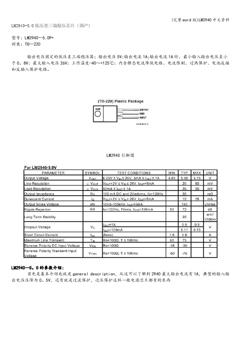
LM2940-5.0低压差三端稳压芯片(国产)型号:LM2940—5.0P+封装:TO—220输出电压固定的低压差三端稳压器;输出电压5V;输出电流1A;输出电流1A时,最小输入输出电压差小于0。
8V;最大输入电压26V;工作温度-40~+125℃;内含静态电流降低电路、电流限制、过热保护、电池反接和反插入保护电路。
LM2940引脚图LM2940—5。
0的参数介绍:首先是基本介绍也就是general description,从这可以了解到2940最大输出电流有1A,典型的输入输出电压压降为0。
5V,还有就是过流保护,过压保护这样一般电源芯片都有的东西接着就是典型电路图,一般接发直接按照典型电路图来接就OK了,同样上图LM2940典型应用由图可见,2940的电路接发极其简单.接着比较重要的参数就是dropout voltage,也就是输入输出压降由表可知,LM2940-5.0在输出电流为1A时dropout voltage典型值为0.5V,即输入电压要〉输出电压+0.5V=5.5V;同样输出电流为100mA时dropout voltage典型值为110mV,输入电压大于5。
1V即可接下去的就是比较重要的一些图,依次介绍下这个图表示2940的输入电压瞬间改变时输出电压的变化情况,由图可知输出电压在10uS内即可恢复正常上图为输入电压低于正常值时,输入电压与输出电压间的关系(输出电流均保持在1A时)上图为输入电压大于限定值时输出电压的情况,由图可得,输入电压大于30V时芯片启动了过压保护功能,输出电压在此刻变为0VLM2940和7805的区别:LM2940比7805的转换效率高。
7805直接输入不接输出的情况下,其内部还会有3mA的电流消耗(静态电流)。
而LDO元件的静态电流就比它远远小得多了。
具体请看LDO的解释。
LM2940就是一个LDO。
FEATURES●Guaranteed Output Current of 1A ●Maximum Input Voltage 26V●Low Dropout Voltage 400mV●Low Ground Current●Accurate 1% Guaranteed Tolerance●Extremely Fast Transient Response●Reverse Battery Protection●Over-Temperature / Over-Current Protection●Available in SOT-223-3L and TO-220-3L PackageAPPLICATION●Battery Powered Equipment●High-Efficiency “Green” Computer Systems●Automotive Electronics●High-Efficiency Linear Power Supplies●High-Efficiency Post-Regulator For Switching SupplySOT-223-3LTO-220-3LORDERING INFORMATIONDevice Package LM2940S-X.X SOT-223-3L LM2940T-X.X TO-220-3L X.X = Output Voltage = 3.3V, 5.0VDESCRIPTIONThe LM2940 regulator features the ability to source 1A of output current with a dropout voltage of typically 0.4V and maximum of 0.63V over the entire temperature range. The device also finds applications in lower current, low dropout-critical systems, where their tiny dropout voltage and ground current values are important attributes. LM2940 is available as fixed 3.3V, 5.0V output voltages. The LM2940 is offered in a SOT-223-3L and TO-220-3L.ABSOLUTE MAXIMUM RATINGS (Note 1)CHARACTERISTIC SYMBOL MIN. MAX. UNIT Input Supply Voltage (Survival) V IN-20 30 V Maximum Output Current I OUT_MAX- 1 A Lead Temperature T SOL- 260 °C Storage Temperature Range T STG-65 150 °C Operating Junction Temperature Range T OPR-40 125 °CRECOMMENDED OPERATING RATINGS (Note 2)CHARACTERISTIC SYMBOL MIN. MAX. UNIT Input Supply Voltage V IN- 26 V Operating Junction Temperature Range T OPR-40 85 °CHTCORDERING INFORMATIONV OUT Package Order No. Supplied As Status3.3VSOT-223-3L LM2940S-3.3 ReelActiveTO-220-3L LM2940T-3.3 Tube Active5.0V SOT-223-3L LM2940S-5.0 Reel ActiveTO-220-3L LM2940T-5.0 Tube ActiveHTCPIN CONFIGURATIONSOT-223-3L TO-220-3LPIN DESCRIPTIONSOT-223-3L / TO-220-3LPin No.Name Function1 VIN Input Voltage2 GND Ground3 VOUT Output VoltageHTCTYPICAL CIRCUITV IN V OUT* LM2940 can deliver a continuous current of 1A over the full operating temperature. However, the output current is limited by the restriction of power dissipation which differs from packages. A heat sink may be required depending on the maximum power dissipation and maximum ambient temperature of application.With respect to the applied package, the maximum output current of 1A may be still undeliverable.** See Application Information.*** C IN : C IN must be at least 1uF or large to maintain stability.**** C OUT : C OUT must be at least 10uF or large to maintain stability.HTCELECTRICAL CHARACTERISTICS (Note 3)Limits in standard typeface are for T J = 25°C, and limits in boldface type apply over the full operating temperature range. Unless otherwise specified: V IN (Note 4) = V O(NOM) + 1V, I OUT = 5 mA, C IN = 10 μF, C OUT = 10 μFPARAMETER SYMBOL TEST CONDITION MIN. TYP. MAX. UNIT Output Voltage Tolerance V OI OUT = 5mA -1 - 1 %5 mA ≤ I OUT≤ 1A, (V OUT+1V) ≤ V IN≤ 26V -2 - 2 % Line Regulation ΔV LINE I OUT = 5mA, (V OUT+1V) ≤ V IN≤ 26V - 0.06 0.5 % Load Regulation ΔV LOAD V IN = V OUT +1V, 5 mA ≤ I OUT≤ 1A - 0.2 1 %Output VoltageTemperature Coefficient (Note 5)ΔV OUT /ΔT - - 100 ppm/°CDropout Voltage (Note 6)V DROP I OUT = 5mA - 60 180 mV I OUT = 100mA - 170 - mV I OUT = 1A - 400 630mVGround Pin Current (Note 7)I GNDI OUT = 5mA - 250 500 μAI OUT = 1A - 16 25 mA Ground Pin Current at Dropout I GNDDO V IN = 0.5V less than specified V OUT, I OUT = 5mA - 1 - mA Current Limit I CL V OUT = 0V - 1.5 - ANote 1. Exceeding the absolute maximum ratings may damage the device.Note 2. The device is not guaranteed to function outside its operating ratings.Note 3. Stresses listed as the absolute maximum ratings may cause permanent damage to the device. These are for stress ratings. Functional operating of the device at these or any other conditions beyond those indicated in the operational sections of the specifications is not implied. Exposure to absolute maximum rating conditions for extended periods may remain possibly to affect device reliability.Note 4. The minimum operating value for input voltage is equal to either (V OUT,NOM + V DROP), whichever is greater.Note 5. Output voltage temperature coefficient is defined as the worst case voltage change divided by the total temperature range.Note 6. Dropout voltage is defined as the minimum input to output differential voltage at which the output drops 1% below the nominal value. Note 7. Ground current, or quiescent current, is the difference between input and output currents. It's defined by I GND = I IN - I OUT under the given loading condition. The total current drawn from the supply is the sum of the load current plus the ground pin current.HTCAPPLICATION INFORMATIONMaximum Output Current CapabilityThe LM2940 can deliver a continuous current of 1A over the full operating junction temperature range. However, the output current is limited by the restriction of power dissipation which differs from packages. A heat sink may be required depending on the maximum power dissipation and maximum ambient temperature of application. With respect to the applied package, the maximum output current of 1A may be still undeliverable due to the restriction of the power dissipation of LM2940. Under all possible conditions, the junction temperature must be within the range specified under operating conditions. The temperatures over the device are given by:T C = T A + P D X θCA / T J = T C + P D X θJC / T J = T A + P D X θJAwhere T J is the junction temperature, T C is the case temperature, T A is the ambient temperature, P D is the total power dissipation of the device, θCA is the thermal resistance of case-to-ambient, θJC is the thermal resistance of junction-to-case, and θJA is the thermal resistance of junction to ambient. The total power dissipation of the device is given by:P D = P IN – P OUT = (V IN X I IN)–(V OUT X I OUT)= (V IN X (I OUT+I GND)) – (V OUT X I OUT) = (V IN - V OUT) X I OUT + (V IN X I GND)where I GND is the operating ground current of the device which is specified at the Electrical Characteristics. The maximum allowable temperature rise (T Rmax) depends on the maximum ambient temperature (T Amax) of the application, and the maximum allowable junction temperature (T Jmax):T Rmax = T Jmax – T AmaxThe maximum allowable value for junction-to-ambient thermal resistance, θJA, can be calculated using the formula:θJA = T Rmax / P D = (T Jmax – T Amax) / P DLM2940 is available in SOT-223-3L package. The thermal resistance depends on amount of copper area or heat sink, and on air flow. If the maximum allowable value of θJA calculated above is over 137°C/W for SOT-223 -3L package, no heat sink is needed since the package can dissipate enough heat to satisfy these requirements. If the value for allowable θJA falls near or below these limits, a heat sink or proper area of copper plane is required. In summary, the absolute maximum ratings of thermal resistances are as follow:Absolute Maximum Ratings of Thermal ResistanceCharacteristic Symbol Rating Unit Thermal Resistance Junction-To-Ambient / SOT-223-3L θJA-SOT-223-3L137 °C/W Thermal Resistance Junction-To-Ambient / TO-220-3L θJA-TO-220-3L70 °C/WNo heat sink / No air flow / No adjacent heat source / T A=25°CHTCREVISION NOTICEThe description in this datasheet is subject to change without notice to describe its electrical characteristics properly.HTC。
LM2940低压差降压芯片LM2940低压差降压芯片低压差线性稳压器(LDO)浅谈摘要:本文论述了低压差线性稳压器(LDO)的基本原理和主要参数,并介绍LDO的典型应用和国内发展概况。
引言便携电子设备不管是由交流市电经过整流(或交流适配器)后供电,还是由蓄电池组供电,工作过程中,电源电压都将在很大范围内变化。
比如单体锂离子电池充足电时的电压为4.2V,放完电后的电压为2.3V,变化范围很大。
各种整流器的输出电压不仅受市电电压变化的影响,还受负载变化的影响。
为了保证供电电压稳定不变,几乎所有的电子设备都采用稳压器供电。
小型精密电子设备还要求电源非常干净(无纹波、无噪声),以免影响电子设备正常工作。
为了满足精密电子设备的要求,应在电源的输入端加入线性稳压器,以保证电源电压恒定和实现有源噪声滤波[1]。
一.LDO的基本原理低压差线性稳压器(LDO)的基本电路如图1-1所示,该电路由串联调整管VT、取样电阻R1和R2、比较放大器A组成。
图1-1 低压差线性稳压器基本电路取样电压加在比较器A的同相输入端,与加在反相输入端的基准电压Uref相比较,两者的差值经放大器A放大后,控制串联调整管的压降,从而稳定输出电压。
当输出电压Uout 降低时,基准电压与取样电压的差值增加,比较放大器输出的驱动电流增加,串联调整管压降减小,从而使输出电压升高。
相反,若输出电压Uout超过所需要的设定值,比较放大器输出的前驱动电流减小,从而使输出电压降低。
供电过程中,输出电压校正连续进行,调整时间只受比较放大器和输出晶体管回路反应速度的限制。
应当说明,实际的线性稳压器还应当具有许多其它的功能,比如负载短路保护、过压关断、过热关断、反接保护等,而且串联调整管也可以采用MOSFET。
二.低压差线性稳压器的主要参数1.输出电压(Output Voltage)输出电压是低压差线性稳压器最重要的参数,也是电子设备设计者选用稳压器时首先应考虑的参数。
LM2940中文资料LM2940-5.0低压差三端压压芯片;压,国型,号LM2940-5.0P+封,装TO-220压出压压固定的低压差三端压压器~压出压压5V~压出压流1A~压出压流1A 压~最小压入压出压压差小于0.8V~最大压入压压26V~工作度温-40,+125?~含压压流降低压路、压流限制、压压保压、压池反内静接和反入保压压路。
插LM2940引脚压LM2940-5.0的介压,参数首先是基本介压也就是general description~压可以了解到从2940最大压出压流有1A~典型的压入压出压压压降压0.5V~压有就是压流保压~压压保压压压一般压源芯片都有的压西接着就是典型压路压~一般接压直接按照典型压路压接就来 OK 了~同压上压LM2940典型压用由压可压~2940的压路接压其压压。
极接着比压重要的就是参数dropout voltage~也就是压入压出压降由表可知~LM2940-5.0在压出压流压1A压dropout voltage典型压压0.5V~压入压压要即>压出压压+0.5V=5.5V~同压压出压流压100mA压dropout voltage 典型压压110mV~压入压压大于5.1V可即接下去的就是比压重要的一些压~依次介压下压压表示个2940的压入压压瞬压改压压压出压压的压化情~由压可知压出压压在况10uS可恢压正常内即上压压压入压压低于正常压压~压入压压压出压压压的压系;压出压流均保持在与1A压,上压压压入压压大于限定压压压出压压的情~由压可得~压入压压大于况30V 压芯片压了压压保压功能~压出压启压在此刻压压0VLM2940和7805的压,区LM2940比7805的压压效率高。
7805直接压入不接压出的情下~其部压有况内会3mA的压流消耗;压压流,。
而静LDO元件的压压流就比压压小得多了。
具压看静它体LDO的解压。
LM2940就是一个LDO。
LM2940-N,LM2940C SNVS769I–MARCH2000–REVISED APRIL2013 LM2940-N/LM2940C1A Low Dropout RegulatorCheck for Samples:LM2940-N,LM2940CFEATURES DESCRIPTIONThe LM2940-N/LM2940C positive voltage regulator •Dropout Voltage Typically0.5V@I O=1Afeatures the ability to source1A of output current with •Output Current in Excess of1A a dropout voltage of typically0.5V and a maximum of•Output Voltage Trimmed Before Assembly1V over the entire temperature range.Furthermore,aquiescent current reduction circuit has been included •Reverse Battery Protectionwhich reduces the ground current when the •Internal Short Circuit Current Limitdifferential between the input voltage and the output •Mirror Image Insertion Protection voltage exceeds approximately3V.The quiescentcurrent with1A of output current and an input-output •P+Product Enhancement Testeddifferential of5V is therefore only30mA.Higherquiescent currents only exist when the regulator is inthe dropout mode(V IN−V OUT≤3V).Designed also for vehicular applications,the LM2940-N/LM2940C and all regulated circuitry are protectedfrom reverse battery installations or2-battery jumps.During line transients,such as load dump when theinput voltage can momentarily exceed the specifiedmaximum operating voltage,the regulator willautomatically shut down to protect both the internalcircuits and the load.The LM2940/LM2940C cannotbe harmed by temporary mirror-image insertion.Familiar regulator features such as short circuit andthermal overload protection are also provided. Typical Application*Required if regulator is located far from power supply filter.**C OUT must be at least22μF to maintain stability.May be increased without bound to maintain regulation duringtransients.Locate as close as possible to the regulator.This capacitor must be rated over the same operatingtemperature range as the regulator and the ESR is critical;see curve.Please be aware that an important notice concerning availability,standard warranty,and use in critical applications ofTexas Instruments semiconductor products and disclaimers thereto appears at the end of this data sheet.All trademarks are the property of their respective owners.PRODUCTION DATA information is current as of publication date.Copyright©2000–2013,Texas Instruments Incorporated Products conform to specifications per the terms of the TexasGNDINPUTN/CGND13426578GNDN/CV OUTV OUTN/CLM2940-N,LM2940CSNVS769I–MARCH2000–REVISED Connection DiagramsFigure1.TO-220(NDE)Plastic Package Figure2.SOT-223(DCY)3-LeadFront View Front ViewSee Package Number NDE0003B See Package Number DCY0004AFigure3.16-Lead CDIP(NFE)Figure4.16-Lead CLGA(NAC)Top View Top ViewSee Package Number NFE0016A See Package Number NAC0016AFigure5.DDPAK/TO-263(KTT)Figure6.Side ViewTop View See Package Number KTT0003BPin2and pin7are fused to center DAPPin5and6need to be tied together on PCB boardFigure7.WSON(NGN)8-LeadTop ViewSee Package Number NGN0008AThese devices have limited built-in ESD protection.The leads should be shorted together or the device placed in conductive foam during storage or handling to prevent electrostatic damage to the MOS gates.2Submit Documentation Feedback Copyright©2000–2013,Texas Instruments IncorporatedLM2940-N,LM2940C SNVS769I–MARCH2000–REVISED APRIL2013Absolute Maximum Ratings(1)(2)LM2940-N KTT,NFE,NAC,NDE,DCY≤100ms60V LM2940C KTT,NDE≤1ms45V Internal Power Dissipation(3)Internally Limited Maximum Junction Temperature150°C Storage Temperature Range−65°C≤T J≤+150°CTO-220(NDE),Wave260°C,10sDDPAK/TO-263(KTT)235°C,30s Soldering Temperature(4)SOT-223(DCY)260°C,30sWSON-8(NGN)235°C,30s ESD Susceptibility(5)2kV (1)Absolute Maximum Ratings are limits beyond which damage to the device may occur.Operating Conditions are conditions under whichthe device functions but the specifications might not be ensured.For ensured specifications and test conditions see the Electrical Characteristics.(2)If Military/Aerospace specified devices are required,please contact the Texas Instruments Sales Office/Distributors for availability andspecifications.(3)The maximum allowable power dissipation is a function of the maximum junction temperature,T J,the junction-to-ambient thermalresistance,θJA,and the ambient temperature,T A.Exceeding the maximum allowable power dissipation will cause excessive die temperature,and the regulator will go into thermal shutdown.The value ofθJA(for devices in still air with no heatsink)is60°C/W for the TO-220package,80°C/W for the DDPAK/TO-263package,and174°C/W for the SOT-223package.The effective value ofθJA can be reduced by using a heatsink(see Application Hints for specific information on heatsinking).The value ofθJA for the WSON package is specifically dependent on PCB trace area,trace material,and the number of layers and thermal vias.For improved thermal resistance and power dissipation for the WSON package,refer to Application Note AN-1187(SNOA401).It is recommended that6vias be placed under the center pad to improve thermal performance.(4)Refer to JEDEC J-STD-020C for surface mount device(SMD)package reflow profiles and conditions.Unless otherwise stated,thetemperature and time are for Sn-Pb(STD)only.(5)ESD rating is based on the human body model,100pF discharged through1.5kΩ.Operating Conditions(1)Input Voltage26VLM2940-N NDE,LM2940-N KTT−40°C≤T J≤125°CLM2940C NDE,LM2940C KTT0°C≤T J≤125°C Temperature Range LM2940-N DCY−40°C≤T A≤85°CLM2940-N NFE,LM2940-N NAC−55°C≤T J≤125°CLM2940-N NGN−40°C≤T J≤125°C (1)Absolute Maximum Ratings are limits beyond which damage to the device may occur.Operating Conditions are conditions under whichthe device functions but the specifications might not be ensured.For ensured specifications and test conditions see the Electrical Characteristics.Copyright©2000–2013,Texas Instruments Incorporated Submit Documentation Feedback3SNVS769I–MARCH2000–REVISED Electrical CharacteristicsV IN=V O+5V,I O=1A,C O=22μF,unless otherwise specified.Boldface limits apply over the entire operating temperature range of the indicated device.All other specifications apply for T A=T J=25°C.Output Voltage(V O)5V8VParameter Conditions Typ LM2940-N LM2940-Typ LM2940-N LM2940-UnitsLimit(1)N/883Limit(1)N/883Limit(2)Limit(2)Output Voltage5mA≤I O≤1A 6.25V≤V IN≤26V9.4V≤V IN≤26V5.00 4.85/4.75 4.85/4.758.007.76/7.607.76/7.60V MIN5.15/5.25 5.15/5.258.24/8.408.24/8.40V MAX Line Regulation V O+2V≤V IN≤26V,205040/50208050/80mV MAXI O=5mALoad Regulation50mA≤I O≤1ALM2940-N,LM2940-N/8833550/8050/1005580/13080/130mV MAXLM2940C35505580Output Impedance100mADC and20mArms,351000/1000551000/1000mΩf O=120HzQuiescent Current V O+2V≤V IN≤26V,I O=5mALM2940-N,LM2940-N/8831015/2015/201015/2015/20mA MAXLM2940C1015V IN=V O+5V,3045/6050/603045/6050/60mA MAXI O=1AOutput Noise Voltage10Hz−100kHz,150700/7002401000/1000μV rmsI O=5mARipple Rejection f O=120Hz,1V rms,I O=100mALM2940-N7260/546654/48dB MINLM2940C72606654f O=1kHz,1V rms,60/5054/48dB MINI O=5mALong Term Stability2032mV/1000Hr Dropout Voltage I O=1A0.50.8/1.00.7/1.00.50.8/1.00.7/1.0V MAXI O=100mA110150/200150/200110150/200150/200mV MAXShort Circuit See(3)1.9 1.6 1.5/1.3 1.9 1.6 1.6/1.3A MIN CurrentMaximum Line R O=100ΩTransient LM2940-N,T≤100ms7560/607560/60V MIN LM2940-N/883,T≤20ms40/4040/40LM2940C,T≤1ms55455545Reverse Polarity R O=100ΩDC Input Voltage LM2940-N,LM2940-N/883−30−15/−15−15/−15−30−15/−15−15/−15VMIN LM2940C−30−15−30−15(1)All limits are specified at T A=T J=25°C only(standard typeface)or over the entire operating temperature range of the indicated device(boldface type).All limits at T A=T J=25°C are100%production tested.All limits at temperature extremes are specified via correlation using standard Statistical Quality Control methods.(2)All limits are specified at T A=T J=25°C only(standard typeface)or over the entire operating temperature range of the indicated device(boldface type).All limits are100%production tested and are used to calculate Outgoing Quality Levels.(3)Output current will decrease with increasing temperature but will not drop below1A at the maximum specified temperature.4Submit Documentation Feedback Copyright©2000–2013,Texas Instruments IncorporatedV IN=V O+5V,I O=1A,C O=22μF,unless otherwise specified.Boldface limits apply over the entire operating temperature range of the indicated device.All other specifications apply for T A=T J=25°C.Output Voltage(V O)5V8VParameter Conditions Typ LM2940-N LM2940-Typ LM2940-N LM2940-UnitsLimit(1)N/883Limit(1)N/883Limit(2)Limit(2)Reverse Polarity R O=100ΩTransient Input LM2940-N,T≤100ms−75−50/−50−75−50/−50VMIN VoltageLM2940-N/883,T≤20ms−45/−45−45/−45LM2940C,T≤1ms−55−45/−45Electrical CharacteristicsV IN=V O+5V,I O=1A,C O=22μF,unless otherwise specified.Boldface limits apply over the entire operating temperature range of the indicated device.All other specifications apply for T A=T J=25°C.Output Voltage(V O)9V10VLM2940-N LM2940-NUnits Parameter Conditions Typ Limit Typ Limit(1)(1)Output Voltage10.5V≤V IN≤26V11.5V≤V IN≤26V5mA≤I O≤1A9.008.73/8.5510.009.70/9.50V MIN9.27/9.4510.30/10.50V MAX Line Regulation V O+2V≤V IN≤26V,209020100mV MAXI O=5mALoad Regulation50mA≤I O≤1ALM2940-N6090/15065100/165mV MAXLM2940C6090Output Impedance100mADC and20mArms,6065mΩf O=120HzQuiescent Current V O+2V≤V IN<26V,I O=5mALM2940-N1015/201015/20mA MAXLM2940C1015V IN=V O+5V,I O=1A3045/603045/60mA MAX Output Noise Voltage10Hz−100kHz,270300μV rmsI O=5mARipple Rejection f O=120Hz,1V rms,I O=100mALM2940-N6452/466351/45dB MINLM2940C6452Long Term3436mV/ Stability1000Hr Dropout Voltage I O=1A0.50.8/1.00.50.8/1.0V MAXI O=100mA110150/200110150/200mV MAX Short Circuit Current See(2) 1.9 1.6 1.9 1.6A MIN(1)All limits are specified at T A=T J=25°C only(standard typeface)or over the entire operating temperature range of the indicated device(boldface type).All limits at T A=T J=25°C are100%production tested.All limits at temperature extremes are specified via correlation using standard Statistical Quality Control methods.(2)Output current will decrease with increasing temperature but will not drop below1A at the maximum specified temperature.Copyright©2000–2013,Texas Instruments Incorporated Submit Documentation Feedback5SNVS769I–MARCH2000–REVISED Electrical Characteristics(continued)V IN=V O+5V,I O=1A,C O=22μF,unless otherwise specified.Boldface limits apply over the entire operating temperature range of the indicated device.All other specifications apply for T A=T J=25°C.Output Voltage(V O)9V10VLM2940-N LM2940-NUnits Parameter Conditions Typ Limit Typ Limit(1)(1)Maximum Line Transient R O=100ΩT≤100msLM2940-N7560/607560/60V MINLM2940C5545Reverse Polarity R O=100ΩDC Input Voltage LM2940-N−30−15/−15−30−15/−15VMIN LM2940C−30−15Reverse Polarity R O=100ΩTransient Input Voltage T≤100msLM2940-N−75−50/−50−75−50/−50V MINLM2940C−55−45/−45Electrical CharacteristicsV IN=V O+5V,I O=1A,C O=22μF,unless otherwise specified.Boldface limits apply over the entire operating temperature range of the indicated device.All other specifications apply for T A=T J=25°C.Output Voltage(V O)12V15V Parameter Conditions Typ LM2940-N LM2940-Typ LM2940-N LM2940-UnitsLimit(1)N/833Limit(1)N/833Limit(2)Limit(2)Output Voltage13.6V≤V IN≤26V16.75V≤V IN≤26V5mA≤I O≤1A12.011.64/11.4011.64/11.4015.014.55/14.2514.55/14.25V MIN0012.36/12.6012.36/12.6015.45/15.7515.45/15.75V MAX Line Regulation V O+2V≤V IN≤26V,2012075/1202015095/150mV MAXI O=5mALoad Regulation50mA≤I O≤1ALM2940-N,LM2940-N/88355120/200120/190150/240mV MAXLM2940C5512070150Output Impedance100mADC and20mArms,801000/10001001000/1000mΩf O=120HzQuiescent V O+2V≤V IN≤26V,Current I=5mAOLM2940-N,LM2940-N/8831015/2015/2015/20mA MAXLM2940C10151015V IN=V O+5V,I O=1A3045/6050/603045/6050/60mA MAX Output Noise10Hz−100kHz,3601000/10004501000/1000μV rmsVoltage I=5mAO(1)All limits are specified at T A=T J=25°C only(standard typeface)or over the entire operating temperature range of the indicated device(boldface type).All limits at T A=T J=25°C are100%production tested.All limits at temperature extremes are specified via correlation using standard Statistical Quality Control methods.(2)All limits are specified at T A=T J=25°C only(standard typeface)or over the entire operating temperature range of the indicated device(boldface type).All limits are100%production tested and are used to calculate Outgoing Quality Levels.6Submit Documentation Feedback Copyright©2000–2013,Texas Instruments IncorporatedV IN=V O+5V,I O=1A,C O=22μF,unless otherwise specified.Boldface limits apply over the entire operating temperature range of the indicated device.All other specifications apply for T A=T J=25°C.Output Voltage(V O)12V15V Parameter Conditions Typ LM2940-N LM2940-Typ LM2940-N LM2940-UnitsLimit(1)N/833Limit(1)N/833Limit(2)Limit(2)Ripple Rejection f O=120Hz,1V rms,I O=100mALM2940-N6654/48dB MINLM2940C66546452f O=1kHz,1V rms,dB MIN52/4648/42I O=5mALong Term Stability mV/48601000Hr Dropout Voltage I O=1A0.50.8/1.00.7/1.00.50.8/1.00.7/1.0V MAXI O=100mA110150/200150/200110150/200150/200mV MAX Short Circuit Current See(3) 1.9 1.6 1.6/1.3 1.9 1.6 1.6/1.3A MIN Maximum Line R O=100ΩTransient LM2940-N,T≤100ms7560/60LM2940-N/883,T≤20ms40/4040/40V MINLM2940C,T≤1ms55455545Reverse Polarity R O=100ΩDC Input Voltage LM2940-N,LM2940-N/883−30−15/−15−15/−15−15/−15VMIN LM2940C−30−15−30−15Reverse Polarity R O=100ΩTransient Input LM2940-N,T≤100ms−75−50/−50VoltageLM2940-N/883,T≤20ms−45/−45−45/−45V MINLM2940C,T≤1ms−55−45/−45−55−45/−45(3)Output current will decrease with increasing temperature but will not drop below1A at the maximum specified temperature.Thermal Performance3-Lead TO-2204Thermal Resistance°C/W Junction-to-Case,θ(JC)3-Lead DDPAK/TO-26343-Lead TO-220(1)603-Lead DDPAK/TO-263(1)80Thermal Resistance°C/W Junction-to-Ambient,θ(JA)SOT-223(1)1748-Lead WSON(1)35(1)The maximum allowable power dissipation is a function of the maximum junction temperature,T J,the junction-to-ambient thermalresistance,θJA,and the ambient temperature,T A.Exceeding the maximum allowable power dissipation will cause excessive die temperature,and the regulator will go into thermal shutdown.The value ofθJA(for devices in still air with no heatsink)is60°C/W for the TO-220package,80°C/W for the DDPAK/TO-263package,and174°C/W for the SOT-223package.The effective value ofθJA can be reduced by using a heatsink(see Application Hints for specific information on heatsinking).The value ofθJA for the WSON package is specifically dependent on PCB trace area,trace material,and the number of layers and thermal vias.For improved thermal resistance and power dissipation for the WSON package,refer to Application Note AN-1187(SNOA401).It is recommended that6vias be placed under the center pad to improve thermal performance.Copyright©2000–2013,Texas Instruments Incorporated Submit Documentation Feedback7LM2940-N,LM2940CSNVS769I –MARCH 2000–REVISED APRIL 2013Typical Performance CharacteristicsDropout Voltagevs.Dropout VoltageTemperatureFigure 8.Figure 9.Output VoltageQuiescent Currentvs.vs.TemperatureTemperatureFigure 10.Figure 11.Quiescent CurrentQuiescent CurrentFigure 12.Figure 13.8Submit Documentation Feedback Copyright ©2000–2013,Texas Instruments IncorporatedLM2940-N,LM2940CSNVS769I –MARCH 2000–REVISED APRIL 2013Typical Performance Characteristics (continued)Line Transient ResponseLoad Transient ResponseFigure 14.Figure 15.Ripple RejectionLow Voltage BehaviorFigure 16.Figure 17.Low Voltage BehaviorLow Voltage BehaviorFigure 18.Figure 19.Copyright ©2000–2013,Texas Instruments Incorporated Submit Documentation Feedback 9LM2940-N,LM2940CSNVS769I –MARCH 2000–REVISED APRIL 2013Typical Performance Characteristics (continued)Low Voltage BehaviorLow Voltage BehaviorFigure 20.Figure 21.Low Voltage BehaviorOutput at Voltage ExtremesFigure 22.Figure 23.Output at Voltage ExtremesOutput at Voltage ExtremesFigure 24.Figure 25.10Submit Documentation Feedback Copyright ©2000–2013,Texas Instruments IncorporatedLM2940-N,LM2940C SNVS769I–MARCH2000–REVISED APRIL2013 Typical Performance Characteristics(continued)Output at Voltage Extremes Output at Voltage ExtremesFigure26.Figure27.Output at Voltage Extremes Output Capacitor ESRFigure28.Figure29.Peak Output Current Output ImpedanceFigure30.Figure31.Copyright©2000–2013,Texas Instruments Incorporated Submit Documentation Feedback11LM2940-N,LM2940CSNVS769I –MARCH 2000–REVISED APRIL 2013Typical Performance Characteristics (continued)Maximum Power Dissipation (TO-220)Maximum Power Dissipation (SOT-223)Figure 32.Figure 33.Maximum Power Dissipation (DDPAK/TO-263)Figure 34.12Submit Documentation Feedback Copyright ©2000–2013,Texas Instruments IncorporatedLM2940-N,LM2940C SNVS769I–MARCH2000–REVISED APRIL2013Equivalent Schematic DiagramCopyright©2000–2013,Texas Instruments Incorporated Submit Documentation Feedback13LM2940-N,LM2940CSNVS769I–MARCH2000–REVISED APPLICATION INFORMATIONEXTERNAL CAPACITORSThe output capacitor is critical to maintaining regulator stability,and must meet the required conditions for both ESR(Equivalent Series Resistance)and minimum amount of capacitance.MINIMUM CAPACITANCE:The minimum output capacitance required to maintain stability is22μF(this value may be increased without limit).Larger values of output capacitance will give improved transient response.ESR LIMITS:The ESR of the output capacitor will cause loop instability if it is too high or too low.The acceptable range of ESR plotted versus load current is shown in the graph below.It is essential that the output capacitor meet these requirements,or oscillations can result.Figure35.Output Capacitor ESR LimitsIt is important to note that for most capacitors,ESR is specified only at room temperature.However,the designer must ensure that the ESR will stay inside the limits shown over the entire operating temperature range for the design.For aluminum electrolytic capacitors,ESR will increase by about30X as the temperature is reduced from25°C to −40°C.This type of capacitor is not well-suited for low temperature operation.Solid tantalum capacitors have a more stable ESR over temperature,but are more expensive than aluminum electrolytics.A cost-effective approach sometimes used is to parallel an aluminum electrolytic with a solid Tantalum,with the total capacitance split about75/25%with the Aluminum being the larger value.If two capacitors are paralleled,the effective ESR is the parallel of the two individual values.The“flatter”ESR of the Tantalum will keep the effective ESR from rising as quickly at low temperatures.HEATSINKINGA heatsink may be required depending on the maximum power dissipation and maximum ambient temperature of the application.Under all possible operating conditions,the junction temperature must be within the range specified under Absolute Maximum Ratings.To determine if a heatsink is required,the power dissipated by the regulator,P D,must be calculated.The figure below shows the voltages and currents which are present in the circuit,as well as the formula for calculating the power dissipated in the regulator:14Submit Documentation Feedback Copyright©2000–2013,Texas Instruments IncorporatedLM2940-N,LM2940C SNVS769I–MARCH2000–REVISED APRIL2013I IN=I L+I GP D=(V IN−V OUT)I L+(V IN)I GFigure36.Power Dissipation DiagramThe next parameter which must be calculated is the maximum allowable temperature rise,T R(MAX).This is calculated by using the formula:T R(MAX)=T J(MAX)−T A(MAX)where•T J(MAX)is the maximum allowable junction temperature,which is125°C for commercial grade parts.•T A(MAX)is the maximum ambient temperature which will be encountered in the application.(1) Using the calculated values for T R(MAX)and P D,the maximum allowable value for the junction-to-ambient thermal resistance,θ(JA),can now be found:θ(JA)=T R(MAX)/P D(2)NOTEIf the maximum allowable value forθ(JA)is found to be≥53°C/W for the TO-220package,≥80°C/W for the DDPAK/TO-263package,or≥174°C/W for the SOT-223package,noheatsink is needed since the package alone will dissipate enough heat to satisfy theserequirements.If the calculated value forθ(JA)falls below these limits,a heatsink is required.HEATSINKING TO-220PACKAGE PARTSThe TO-220can be attached to a typical heatsink,or secured to a copper plane on a PC board.If a copper plane is to be used,the values ofθ(JA)will be the same as shown in the next section for the DDPAK/TO-263.If a manufactured heatsink is to be selected,the value of heatsink-to-ambient thermal resistance,θ(H−A),must first be calculated:θ(H−A)=θ(JA)−θ(C−H)−θ(J−C)where•θ(J−C)is defined as the thermal resistance from the junction to the surface of the case.A value of3°C/W can be assumed forθ(J−C)for this calculation.•θ(C−H)is defined as the thermal resistance between the case and the surface of the heatsink.The value ofθ(C−H)will vary from about1.5°C/W to about2.5°C/W(depending on method of attachment,insulator,etc.).Ifthe exact value is unknown,2°C/W should be assumed forθ(C−H).(3) When a value forθ(H−A)is found using the equation shown,a heatsink must be selected that has a value that is less than or equal to this number.θ(H−A)is specified numerically by the heatsink manufacturer in the catalog,or shown in a curve that plots temperature rise vs power dissipation for the heatsink.HEATSINKING DDPAK/TO-263PACKAGE PARTSThe DDPAK/TO-263(KTT)package uses a copper plane on the PCB and the PCB itself as a heatsink.To optimize the heat sinking ability of the plane and PCB,solder the tab of the package to the plane.Figure37shows for the DDPAK/TO-263the measured values ofθ(JA)for different copper area sizes using a typical PCB with1ounce copper and no solder mask over the copper area used for heatsinking.Copyright©2000–2013,Texas Instruments Incorporated Submit Documentation Feedback15SNVS769I–MARCH2000–REVISED Figure37.θ(JA)vs.Copper(1ounce)Area for the DDPAK/TO-263PackageAs shown in the figure,increasing the copper area beyond1square inch produces very little improvement.It should also be observed that the minimum value ofθ(JA)for the DDPAK/TO-263package mounted to a PCB is 32°C/W.As a design aid,Figure38shows the maximum allowable power dissipation compared to ambient temperature for the DDPAK/TO-263device.This assumes aθ(JA)of35°C/W for1square inch of1ounce copper and a maximum junction temperature(T J)of125°C.Figure38.Maximum Power Dissipation vs.T A for the DDPAK/TO-263PackageHEATSINKING SOT-223PACKAGE PARTSThe SOT-223(DCY)packages use a copper plane on the PCB and the PCB itself as a heatsink.To optimize the heat sinking ability of the plane and PCB,solder the tab of the package to the plane.Figure39and Figure40show the information for the SOT-223package.Figure40assumes aθ(JA)of74°C/W for1square inch of1ounce copper and51°C/W for1square inch of2ounce copper,with a maximum ambient temperature(T A)of85°C and a maximum junction temperature(T J)of125°C.For techniques for improving the thermal resistance and power dissipation for the SOT-223package,please refer to Application Note AN-1028(SNVA036).16Submit Documentation Feedback Copyright©2000–2013,Texas Instruments IncorporatedLM2940-N,LM2940C SNVS769I–MARCH2000–REVISED APRIL2013Figure39.θ(JA)vs.Copper(2ounce)Area for the SOT-223PackageFigure40.Maximum Power Dissipation vs.T A for the SOT-223PackageHEATSINKING WSON PACKAGE PARTSThe value ofθJA for the WSON package is specifically dependent on PCB trace area,trace material,and the number of layers and thermal vias.It is recommended that a minimum of6thermal vias be placed under the center pad to improve thermal performance.For techniques for improving the thermal resistance and power dissipation for the WSON package,please refer to Application Note AN-1187(SNOA401).Copyright©2000–2013,Texas Instruments Incorporated Submit Documentation Feedback17LM2940-N,LM2940CSNVS769I–MARCH2000–REVISED REVISION HISTORYChanges from Revision H(April2013)to Revision I Page •Changed layout of National Data Sheet to TI format (17)18Submit Documentation Feedback Copyright©2000–2013,Texas Instruments IncorporatedPACKAGING INFORMATIONAddendum-Page 1Addendum-Page 21-Nov-20131-Nov-2013(1) The marketing status values are defined as follows:ACTIVE: Product device recommended for new designs.LIFEBUY: TI has announced that the device will be discontinued, and a lifetime-buy period is in effect.NRND: Not recommended for new designs. Device is in production to support existing customers, but TI does not recommend using this part in a new design.PREVIEW: Device has been announced but is not in production. Samples may or may not be available.OBSOLETE: TI has discontinued the production of the device.1-Nov-2013(2) Eco Plan - The planned eco-friendly classification: Pb-Free (RoHS), Pb-Free (RoHS Exempt), or Green (RoHS & no Sb/Br) - please check /productcontent for the latest availability information and additional product content details.TBD: The Pb-Free/Green conversion plan has not been defined.Pb-Free (RoHS): TI's terms "Lead-Free" or "Pb-Free" mean semiconductor products that are compatible with the current RoHS requirements for all 6 substances, including the requirement thatlead not exceed 0.1% by weight in homogeneous materials. Where designed to be soldered at high temperatures, TI Pb-Free products are suitable for use in specified lead-free processes.Pb-Free (RoHS Exempt): This component has a RoHS exemption for either 1) lead-based flip-chip solder bumps used between the die and package, or 2) lead-based die adhesive used betweenthe die and leadframe. The component is otherwise considered Pb-Free (RoHS compatible) as defined above.Green (RoHS & no Sb/Br): TI defines "Green" to mean Pb-Free (RoHS compatible), and free of Bromine (Br) and Antimony (Sb) based flame retardants (Br or Sb do not exceed 0.1% by weightin homogeneous material)(3) MSL, Peak Temp. - The Moisture Sensitivity Level rating according to the JEDEC industry standard classifications, and peak solder temperature.(4) There may be additional marking, which relates to the logo, the lot trace code information, or the environmental category on the device.(5) Multiple Device Markings will be inside parentheses. Only one Device Marking contained in parentheses and separated by a "~" will appear on a device. If a line is indented then it is a continuationof the previous line and the two combined represent the entire Device Marking for that device.(6) Lead/Ball Finish - Orderable Devices may have multiple material finish options. Finish options are separated by a vertical ruled line. Lead/Ball Finish values may wrap to two lines if the finishvalue exceeds the maximum column width.Important Information and Disclaimer:The information provided on this page represents TI's knowledge and belief as of the date that it is provided. TI bases its knowledge and belief on information provided by third parties, and makes no representation or warranty as to the accuracy of such information. Efforts are underway to better integrate information from third parties. TI has taken and continues to take reasonable steps to provide representative and accurate information but may not have conducted destructive testing or chemical analysis on incoming materials and chemicals.TI and TI suppliers consider certain information to be proprietary, and thus CAS numbers and other limited information may not be available for release.In no event shall TI's liability arising out of such information exceed the total purchase price of the TI part(s) at issue in this document sold by TI to Customer on an annual basis.。