M3225 24M 晶体 晶振规格书
- 格式:doc
- 大小:84.50 KB
- 文档页数:3


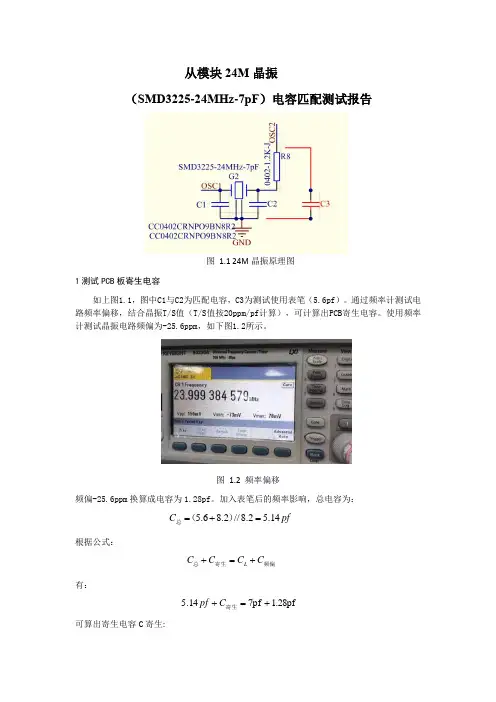
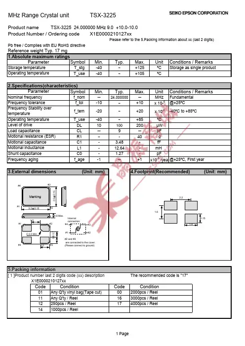
从模块24M 晶振(SMD3225-24MHz -7pF )电容匹配测试报告图 1.1 24M 晶振原理图 1测试PCB 板寄生电容如上图1.1,图中C1与C2为匹配电容,C3为测试使用表笔(5.6pf )。
通过频率计测试电路频率偏移,结合晶振T/S 值(T/S 值按20ppm/pf 计算),可计算出PCB 寄生电容。
使用频率计测试晶振电路频偏为-25.6ppm ,如下图1.2所示。
图 1.2 频率偏移频偏-25.6ppm 换算成电容为1.28pf 。
加入表笔后的频率影响,总电容为:pf C 14.52.8//2.86.5=+=)(总根据公式:L C C C C +=+总频偏寄生有:1.28pf 7pf 14.5+=+寄生C pf可算出寄生电容C 寄生:pf 14.3=寄生C2.根据寄生电容值进行匹配方案设计使用的晶振为24.000MHz,CL=7pf 。
根据C 寄生的取值,能够优化出以下几个备选方案:表 1不同匹配电容的备选方案可见方案B 串联后容值匹配效果较好。
已知匹配电容C1=C2=8.2pf ,表笔电容5.6pf ,晶振的T/S=20ppm/pf ,接下来可计算出实际的频率偏移。
使用表笔(5.6pf )测试出晶振电路频偏为-25.6ppm ,计算此时电路实配电容:14.52C 1C 2C 1C =++•+表笔表笔)(C C pf同时,计算不加表笔时匹配电容:pf C C 1.42//1=表笔令整个电路的匹配电容增加1.04pf ,即频偏增加了20.8ppm ,根据“电容容值越大,晶振电路频率越低”的原理,可得出电路未引入表笔时频偏为-4.8ppm 。
3. 测试方案B 的波形和特性阻抗。
图 1.3 方案B 芯片输入波形图 1.4 方案B芯片输出波形负阻抗测试,约1.5K欧姆时,不能正常抄表。
查规格书,等效电阻最大约为50欧姆,阻抗值为等效阻抗30倍,合理。
4.之前使用以下原理,未串入电阻,匹配电容10pf时输入存在明显过冲,输出波形畸变较为严重。
3225晶振技术参数和
外部尺寸图
本页仅作为文档封面,使用时可以删除
This document is for reference only-rar21year.March
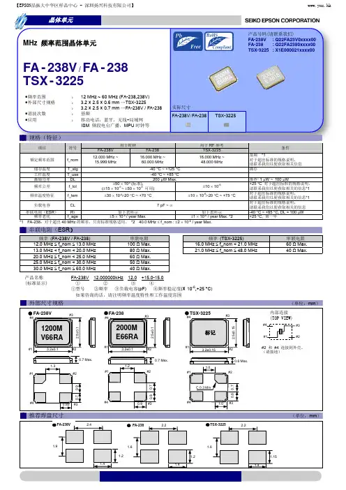
3225晶振是贴片晶振中的一种封装尺寸,3225晶振又分为有源贴片3225晶振和无源贴片3225晶振,这两种可以做的频率是不一样的,有源贴片3225晶振最低可以做到1MHZ,但无源贴片3225晶振目前为止最低只能做到12MHZ下面为大家分别介绍两种晶振的参数可广泛应用于通讯数码电子,消费类电子,汽车电子等领域,其技术参数和封装尺寸如下:
3225无源贴片晶振技术参数表:
3225无源贴片晶振外尺寸图:
3225有源贴片晶振技术参数表:
3225有源贴片晶振外尺寸图。
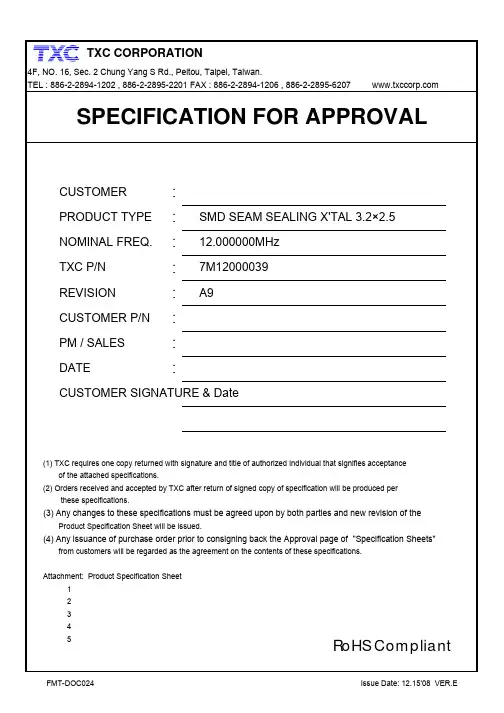
(1) TXC requires one copy returned with signature and title of authorized individual that signifies acceptanceof the attached specifications.(2) Orders received and accepted by TXC after return of signed copy of specification will be produced perthese specifications.(3) Any changes to these specifications must be agreed upon by both parties and new revision of theProduct Specification Sheet will be issued.(4) Any issuance of purchase order prior to consigning back the Approval page of "Specification Sheets"from customers will be regarded as the agreement on the contents of these specifications.Attachment: Product Specification Sheet12345CUSTOMER SIGNATURE & DateDATE:PM / SALES :CUSTOMER P/N :REVISION :A9TXC P/N:7M12000039NOMINAL FREQ.:12.000000MHz PRODUCT TYPE :SMD SEAM SEALING X'TAL 3.2×2.5RoHS CompliantTEL : 886-2-2894-1202 , 886-2-2895-2201 FAX : 886-2-2894-1206 , 886-2-2895-6207 SPECIFICATION FOR APPROVALCUSTOMER :TEL : 886-2-2894-1202 , 886-2-2895-2201 FAX : 886-2-2894-1206 , 886-2-2895-6207 25-May-09A82ECN-08P123001A93,4ECN-09P052503RevRevise pageRevise contentsDateRef.No.A1N/A ReviserInitial released7-Nov-07N/AYachuan MiaoYachuan Miao Package Change25-May-09Yachuan MiaoRr Change: 200 ohm to 100 ohm 30-Dec-08ELECTRICAL SPECIFICATIONSStandard atmospheric conditionsUnless otherwise specified, the standard range of atmospheric conditions for making measurement and tests are as follow:Ambient temperature :25±5 Relative humidity:40%~70%If there is any doubt about the results, measurement shall be made within the following limits:Ambient temperature :25±3 Relative humidity :40%~70%Measure equipmentElectrical characteristics measured by HP E5100A or equivalent.Crystal cutting typeThe crystal is using AT CUT (thickness shear mode). Unit Weight: 0.018±0.001 g/pcs1Nominal Frequency 2Oscillation Mode 3Load Capacitance 4Frequency Tolerance 5Frequency Stability 6Operating Temperature 7Aging 8Drive Level9Effective Resistance Rr 10Shunt Capacitance C011Insulation Resistance 12Storage Temperature Range--30~85at 25 ± 3±20ppm Over Operating Temp. Range (Reference 25 )ppm -ParametersSYM.Electrical Spec.MINTYPE MAXUNITS -±20--FundamentalMHz CL 18pF -Notes FL 12.000000-- -1st Year -ppm Ω-DL µW --10-Rr -100-±5--~C0--pF 5M Ω at DC 100V -50085---40。