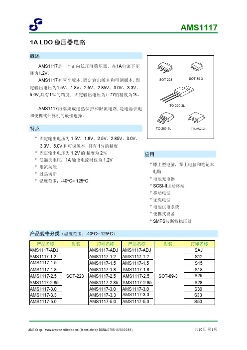
AMS1117引脚图
- 格式:doc
- 大小:77.51 KB
- 文档页数:3
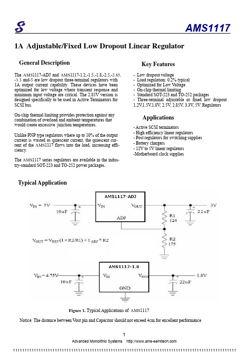
1A Adjustable/Fixed Low Dropout Linear Regulator- Low dropout voltage- Load regulation: 0.2% typical - Optimized for Low V oltage - On-chip thermal limiting- Standard SOT-223 and TO-252 packages- Three-terminal adjustable or fixed low dropout 1.2V ,1.5V ,1.8V , 2.5V , 2.85V , 3.3V , 5V . Regulators- Active SCSI terminators- High efficiency linear regulators- Post regulators for switching supplies - Battery chargers- 12V to 5V linear regulators - M otherboard clock suppliesThe AMS 1117-ADJ and AMS 1117-1.2,-1.5,-1.8,-2.5,-2.85, -3.3 and-5 are low dropout three-terminal regulators with 1A output current capability. These devices have been optimized for low voltage where transient response and minimum input voltage are critical. The 2.85V version is designed specifically to be used in Active Terminators for SCSI bus.On-chip thermal limiting provides protection against any combination of overload and ambient temperatures that would create excessive junction temperatures.Unlike PNP type regulators where up to 10% of the output current is wasted as quiescent current, the quiescent cur-rent of the AMS 1117 flows into the load, increasing effi-ciency.The AMS 1117 series regulators are available in the indus-try-standard SOT-223 and TO-252 power packages.Key FeaturesApplicationsGeneral DescriptionTypical ApplicationNotice: The distance between V out pin and Capacitor should not exceed 4cm for excellent performanceFigure 1. Typical Applications of AMS 11171A Adjustable/Fixed Low Dropout Linear RegulatorPin Assignments*With package soldered to 0.5 square inch copper area over backside ground plane or internal power plane, ΘJA can vary from 30°C/W to more than 50°C/W. Other mounting techniques may provide better thermal resistance than 30°C/W.Absolute Maximum RatingsFigure 2. Pin Assignments of AMS 1117ParameterMin.Max.UnitV IN 18 V(V IN – V OUT ) * I OUTSee Figure 3Operating Junction Temperature Range -20 125°C Storage Temperature Range-65150°C Lead Temperature (Soldering, 10 sec.) 300°C1A Adjustable/Fixed Low Dropout Linear RegulatorTypicals and limits appearing in normal type apply for T J =25℃.Limits appearing in Boldface type apply over the entire junction temperature for operation, -20℃to 125℃.Electrical CharacteristicBlock DiagramThermal LimitCurrent LimitV OUTV INSubstrateGND (fixed output) ADJ. (adjustable output)Figure 3. Block Diagram of AMS 1117SymbolParameterConditionsMin (Note 2) Typ (Note 1) Max(Note 2)UnitsV REFReference VoltageAMS 11171.5V<=(V IN -V OUT )<=7V,10mA<=I OUT <=1A1.225 1.250 1.275 VV OUT OutputVoltage 10mA<=I OUT <=1AI OUT = 10mA, V IN = 3.2V AMS 1117-1.2 ,2.7V<= V IN <=8.2V 1.176 1.152 1.200 1.200 1.224 1.248 V AMS 1117-1.5 ,3.0V<= V IN <=8.5V1.4701.5001.530VAMS 1117-1.8 ,3.3V<= V IN <=8.8V 1.764 1.800 1.836 VAMS 1117-2.5 ,4V<= V IN <= 9.5V 2.450 2.500 2.550 V AMS 1117-2.85 , 4.35V <= V IN <= 9.85V 2.793 2.850 2.907 V AMS 1117-3.3 , 4.8V<= V IN <=10.3V 3.234 3.300 3.366 V AMS 1117-5.0,6.5V<=V IN <= 12V4.9005.0005.100V1A Adjustable/Fixed Low Dropout Linear RegulatorTypicals and limits appearing in normal type apply for T J =25℃.Limits appearing in Boldface type apply over the entire junction temperature for operation, -20℃ to 125℃.Electrical Characteristic(Continued)SymbolParameter ConditionsMin (Note 2)Typ (Note 1) Max (Note 2) Units △V OUTLine Regultion (Note 3)I OUT =10mA ,(V OUT +1.5V)<=V IN <=12V 0.035 0.2 % Load Regultion (Note 3) V IN -V OUT =2V,10mA<= I OUT <=1A,0.2 0.7 % AMS 1117-1.2V IN -V OUT =2V,10mA<= I OUT <=1A,0.2 1 % V IN -V OUTDropout Volage I OUT =1A,△V REF =1% 1.100 1.250 V I LimitCurrent Limit V IN -V OUT = 2V, T J =25℃1.1 1.5A Minimum Load Current (Note 4) AMS 1117-ADJ1.5V<=(V IN -V OUT )<=10V10mA Quiescent CurentV IN =V OUT +1.25V 5 13 mA Thermal Regulation T A = 25°C, 30ms pulse 0.01 0.1 %/W RippleRejection f=120Hz,V IN -V OUT =3V, V Ripple =1V PP60 72 dB Adjust Pin Current50120µAAdjust Pin CurrentChange 1.5V<=V IN -V OUT <=7V, 10mA<=I OUT <=1A0.2 5 µATemperature Stability0.5 % Long Term StabilityT A = 125°C, 1000hrs.0.3%1A Adjustable/Fixed Low Dropout Linear RegulatorNote 1: Typical Values represent the most likely parametric norm. Note 2: All limits are guaranteed by testing or statistical analysis.Note 3: Load and line regulation are measured at constant junction room temperature. Note 4: The minimum output current required to maintain regulation.Typical Performance CharacteristicsTypicals and limits appearing in normal type apply for T J =25℃.Limits appearing in Boldface type apply over the entire junction temperature for operation, -20℃to 125℃.Electrical Characteristic(Continued)Symbol ParameterConditionsMin (Note 2) Typ (Note 1) Max (Note 2)UnitsI LimitRMS Output Noise(% ofV OUT )T A = 25°C, 10Hz<= f <=10kHz0.003 % Thermal Resistance, Junctionto CaseSOT-223 15 ℃/W TO-252 3 ℃/W Thermal Shutdown Junction Temperature155 ℃ Thermal Shutdown Hysteresis25℃Output Current ( A )0 0.2 0.4 0.6 0.8 1.01.5 1.4 1.3 1.2 1.0 0.9 0.8 0.7 0.6 0.5 0D r o p o u t V o l t a g e ( V )Figure 4. Dropout Voltage VS. Output Current1A Adjustable/Fixed Low Dropout Linear RegulatorTypical Performance Characteristics(Continued)Figure 6. Output Voltage VS. TemperatureO u t p u t V o l t a g e ( V )3.70 3.65 3.603.553.50 3.45 3.40 3.35 3.30 3.253.20Junction Temperature ( ℃ )-75 –50 –25 0 25 50 75 100 125 150 175Figure 5. Reference Voltage VS. TemperatureR e f e r e n c e V o l t a g e ( V )0.260 1.255 1.250 1.245 1.240 1.235 1.225 1.220 1.215 1.210Junction Temperature ( ℃ )-75 –50 –25 0 25 50 75 100 125 150 175Figure 7. Minimum Load Current VS. TemperatureM i n i m u m L o a d C u r r e n t ( m A )5 4 3 2 1Junction Temperature ( ℃ ) -75 –50 –25 0 25 50 75 100 125 150 175Figure 8. ADJ Pin Current VS. TemperatureA D J P i n C u r r e n t ( µA ) 100 90 807060 50 40 30 20 10 0Junction Temperature ( ℃ ) -75 –50 –25 0 25 50 75 100 125 150 175Note:AMS 1117 OnlyAMS11171AAdjustable/Fixed Low Dropout Linear RegulatorMechanical Dimensions4-Lead SOT-223 PackageSymbolInches Millimeters NotesMin.Max.Min. Max.A Ñ .071 Ñ 1.80 A1 Ñ .181 Ñ 4.80B .025 .033 .064 .840 c Ñ 0.90 Ñ 2.29 D .248 .264 6.30 6.71 E .130 .148 3.30 3.71 e .115 .124 2.95 3.15 F .033 .041 .840 1.04 H .264 .287 6.71 7.29 I .0121 Ñ .310 Ñ J Ñ 10° Ñ 10° K 10° 16° 10° 16° L.0008 .0040 .0203 .1018 M 10° 16° 10° 16° N.010.014.250.360Figure 9. 4-Lead SOT-223 Package1A Adjustable/Fixed Low Dropout Linear RegulatorMechanical Dimensions(Continued)3-Lead TO-252 PackageNotes:1. Dimensions are exclusive of mold flash, metal burrsor interlead protrusion.2. Stand off-height is measured from lead tip with ref. toDatum –B-.3. Foot length is measured with ref. to Datum –A– withlead surface. 4. Thermal pad contour optional within dimension b3 and L3.5. Formed leads to be planar with respect to one anotherat seating place –C-.6. Dimensions and tolerances.SymbolInchesMillimetersNotesMin. Max.Min. Max.A .086 .094 2.19 2.39 b .025 .035 0.64 0.89 b2 .030 .045 0.76 1.14 b3 .205 .215 5.12 5.46 4 c .018 .024 0.46 0.61 c2 .018 .023 0.46 0.58 D .210 .245 5.33 6.22 1E .250 .265 6.35 6.73 1e .090 BSC 2.29 BSCH .370 .410 9.40 10.41 L .055 .070 1.40 1.78 3 L1 .108 REF 2.74 REFL3 .035 .080 0.89 2.03 4 L4.025.0400.641.02Figure 10. 3-Lead TO-252 Package1A Adjustable/Fixed Low Dropout Linear R egulatorAdvanced Monolithic Systems The " " logo is a registered trademark of Advanced Monolithic Systems.All other company and product names are trademarks of their respective ownersOrdering InformationPackage Temperature Range Part Number Output Voltage Packing Marking Transport MediaSOT -223-20℃ - +125℃ AMS 1117-1.2 1.2V AMS 1117 1.2 2.5K Tape and Reel -20℃ - +125℃ AMS 1117-1.5 1.5V AMS 1117 1.5 2.5K Tape and Reel -20℃ - +125℃ AMS 1117-1.8 1.8V AMS 1117 1.8 2.5K Tape and Reel-20℃ - +125℃ AMS 1117-2.5 2.5V AMS 1117 2.5 2.5K Tape and Reel -20℃ - +125℃ AMS 1117-2.85 2.85V AMS 1117 2.8 2.5K Tape and Reel -20℃ - +125℃ AMS 1117-3.3 3.3V AMS 1117 3.3 2.5K Tape and Reel -20℃ - +125℃ AMS 1117-5 5V AMS 1117 5 2.5K Tape and Reel -20℃ - +125℃ AMS 1117 Adjust AMS 1117 2.5K Tape and Reel TO -252-20℃ - +125℃ AMS 1117-1.2 1.2V AMS 1117 1.2 2.5K Tape and Reel -20℃ - +125℃ AMS 1117-1.5 1.5V AMS 1117 1.5 2.5K Tape and Reel -20℃ - +125℃ AMS 1117-1.8 1.8V AMS 1117 1.8 2.5K Tape and Reel-20℃ - +125℃ AMS 1117-2.5 2.5V AMS 1117 2.5 2.5K Tape and Reel -20℃ - +125℃ AMS 1117-2.85 2.85V AMS 1117 2.8 2.5K Tape and Reel -20℃ - +125℃ AMS 1117-3.3 3.3V AMS 1117 3.3 2.5K Tape and Reel -20℃ - +125℃ AMS 1117-5 5.0V AMS 1117 5 2.5K Tape and Reel -20℃ - +125℃ AMS 1117CD Adjust AMS 1117CD 2.5K Tape and ReelDisclaimer:• AMS reserves the right to make changes to the information herein for the improvement of the design and performancewithout further notice! Customers should obtain the latest relevant information before placing orders and should verify that such information is complete and current.• All semiconductor products malfunction or fail with some probability under special conditions. When using AMS productsin system design or complete machine manufacturing, it is the responsibility of the buyer to comply with the safety standards strictly and take essential measures to avoid situations in which a malfunction or failure of such AMS products could cause loss of body injury or damage to property.• AMS will supply the best possible product for customers!。


低压差稳压器--AMS1117芯⽚简介结构从内部框图可以看出,ASM1117提供电流限制和热保护(TSD),以防环境温度造成过⾼的结温。
电路包含1个齐纳调节的带隙参考电压以确保输出电压的精度在±1%以内。
ADJ引脚是可调整电压引脚,⽤来接⼊可调电阻,调出你所需要的电压。
基本⼯作原理AMS1117是⼀个低漏失电压调整器,它的稳压调整管是由⼀个PNP驱动的NPN管组成的,漏失电压定义为: VDROP = VBE+ VSAT。
AMS1117有固定和可调两个版本可⽤,输出电压可以是:1.2V,1.5V,1.8V,2.5V,2.85V, 3.0V,3.3V,和5.0V。
⽚内过热切断电路提供了过载和过热保护,以防环境温度造成过⾼的结温。
LM1117有可调电压的版本,通过2个外部电阻可实现1.25~13.8V输出电压范围。
另外还有5个固定电压输出(1.8V、2.5V、2.85V、3.3V和5V)的型号。
X1117是⼀款正电压输出的低压降三端线性稳压电路,在1A输出电流下的压降为1.2V。
分为两个版本,固定电压输出版本和可调电压输出版本。
固定输出电压1.5V、1.8V、2.5V、3.3V、5.0V和可调版本的电压精度为1%;固定电压为1.2V的产品输出电压精度为2%。
内部集成过热保护和限流电路,适⽤于各类电⼦产品。
AMS1117-3.3参数:绝对最⼤额定值:20V⼯作结温范围:-40~125°C输⼊电压:15V焊接温度(25秒):265°C存储温度:-65~150°CAMS1117-3.3电⽓特性:输出电压:3.267~3.333V(0≤IOUT≤1A,4.75V≤VIN≤12V)线性调整(最⼤):10mV(4.75V≤VIN≤12V)负载调节(最⼤):15mV(VIN=5V,0≤IOUT≤1A)电压差(最⼤):1.3V电流限制:900~1500mA静态电流(最⼤):10mA纹波抑制(最⼩):60dB。