mx612 直流电机驱动IC 马达驱动IC
- 格式:pdf
- 大小:1.31 MB
- 文档页数:11
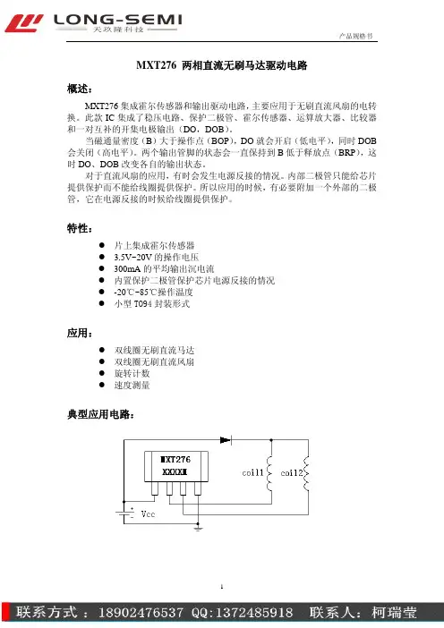
MXT276 两相直流无刷马达驱动电路概述:MXT276集成霍尔传感器和输出驱动电路,主要应用于无刷直流风扇的电转换。
此款IC集成了稳压电路、保护二极管、霍尔传感器、运算放大器、比较器和一对互补的开集电极输出(DO,DOB)。
当磁通量密度(B)大于操作点(BOP),DO就会开启(低电平),同时DOB 会关闭(高电平)。
两个输出管脚的状态会一直保持到B低于释放点(BRP),这时DO、DOB改变各自的输出状态。
对于直流风扇的应用,有时会发生电源反接的情况。
内部二极管只能给芯片提供保护而不能给线圈提供保护。
所以应用的时候,有必要附加一个外部的二极管,它在电源反接的时候给线圈提供保护。
特性:z片上集成霍尔传感器z 3.5V~20V的操作电压z300mA的平均输出沉电流z内置保护二极管保护芯片电源反接的情况z-20℃~85℃操作温度z小型TO94封装形式应用:z双线圈无刷直流马达z双线圈无刷直流风扇z旋转计数z速度测量典型应用电路:内部功能模块示意图:管脚描述:管脚名称管脚顺序P/I/O 描述Vcc 1 P 电源输入DO 2 O 输出驱动DOB 3 O 输出驱动GND 4 P 地绝对最大数据:(25℃)参数特性符号 数值 单位 电源电压 V CC 24 V 极性反接电压 V RCC -20 V磁通量密度 B 无限制 连续 0.3保持0.35输出“on”电流 峰值(启动)I C 0.5 A 工作温度范围 Ta -20~85 ℃ 存贮温度范围 Ts -65~150 ℃ 封装能量耗散 PD 500 mW 最大节温 Tj150 ℃电学特性:特性符号 条件 最小典型 最大 单位输出CE 电压 VceVcc=3.5V,I L =100mA0.2 V 电源电压 Vcc 3.5 20 V 输出饱和电压 Vce (sat)Vcc=14V, I L =300mA 0.3 0.6 V 输出漏电流 Icex Vce=14V,Vcc=14V 11 uA 消耗电流 Icc Vcc=20V,输出开路 16 25 mA 输出上升时间 tr Vcc=12V,R L =820Ω,C L =20pF3 10 us 输出下降时间 tf Vcc=12V,R L =820Ω,C L =20pF0.3 1.5 us 转换时间差 Δt Vcc=12V,R L =820Ω,C L =20pF310us测试电路:磁特性:A级参数 符号 最小 典型 最大 单位 操作点 Bop 10 - 50 高斯 释放点 Brp -50 - -10 高斯 磁滞 Bhy - 55 - 高斯B级参数 符号 最小 典型 最大 单位 操作点 Bop 5 - 70 高斯 释放点 Brp -70 - -5 高斯 磁滞 Bhy - 55 - 高斯C级参数 符号 最小 典型 最大 单位 操作点 Bop - - 100 高斯 释放点 Brp -100 - - 高斯 磁滞 Bhy - 55 - 高斯D级参数 符号 最小 典型 最大 单位 操作点 Bop - - 125 高斯 释放点 Brp -125 - - 高斯 磁滞 Bhy - 55 - 高斯打标信息:。
I.INTRODUCTIONThe microprocessor-controlled Max Charge MC-612 is the most advancedregulator available. Designed to continual-ly monitor battery voltage and automaticallyoptimize charging, the MC-612 uses up to 12 time and voltage increments to ensure your batteries receive a full charge quickly and safely.The MC-612 lets you choose from a variety of selectablepreset programs to best suit your charging needs. II t s U n i v e r s a l F a c t o r y P r og r a m a l l o w s y o u t o c o n n e c t t h e M C -612 t oy o u r a l t e r n a t o r r i g h t o u t o f t h e b o x .Six additional preset programs support most popular battery types, including stan-dard and deep-cycle flooded batteries, AGM, gel, and Optima (spiral wound) technologies, as well as special settings for systems supplying halogen lighting. An easy-to-use magnetic reed switch delivers quick, precise regulator adjustment.Should your charging system require individualized adjustment, the MC-612 provides additional advanced user-defined programming options.When used with optional alternator and battery temperature sensors, the MC-612 automatically monitors ambient alter-nator and battery temperatures and compensates by adjusting field output to match conditions. Alarm outputs connect to audible or visual alarms to provide warnings of dangerous system conditions .II. SAFETY CONSIDERATIONSBefore installing your MC-612 marine regulator, please take a moment to con-sider these guidelines for safe regulator installation. Failure to work safely could result in personal injury or damage to your electrical system.1.Always disconnect your battery banks and ensure that switches are “OFF”prior to installing your regulator.2.Remove loose-fitting clothing or jewelry, which could become entangled inyour motor or other machinery.3.Wear ANSI-approved safety glasses.4.DO NOT attempt to modify the regulator. Alterations could result in damage to your charging system, and will void your warranty.5.Do not attempt installation if tired or fatigued.6.Ensure the engine has cooled before initiating installation.7.Do not attempt installation while using alcohol or any medication that could impair your judgment or reaction time.8.Always use the right tool for the job. Improper tool use may damage the regulator or your boat, and could result in personal injury.9.Take time to read the manual. Equipment damage and possibleinjuries may result from an incomplete understanding of the installa-tion and operation of the MC-612 regulator. If you are unfamiliar with marine electrical systems, consult with a licensed marine electrician.Max Charge MC-612 Regulator Installation and Operator’s ManualThe following information is essential to the proper operation of your Max Charge regulator. Do not install or operate before review-ing the following:1.POSITIVE BATTERY SENSE WIRE- User supplied -- not in harness. This wire must be connected to the regulatorand to a source of positive battery voltage (see Figure 3 for mounting location) to provide proper regulator operation.The regulator WILL NOT WORK if the sense wire is not connected to the regulator or the voltage source. The Positive BATTERY SENSE WIRE MUST BE FUSED. A 1-amp ATC fuse and holder are included with the regulator and harness.2.GROUNDING- The Model MC-612 must be properly grounded to regulate accurately. The two ground wires locatedin the harness must be securely attached to their terminals and at the alternator’s preferred ground to ensure proper grounding. A grounding cable between the alternator and the system ground is strongly recommended.3.VOLTAGE READINGS- MC-612 digital circuitry is engineered to monitor battery charge state and automaticallycompensate for changes in battery voltage during operation. As a result, it is NOT unusual to see near-constant changes in the regulator’s Battery Voltage display. These voltage changes reflect the regulator’s ability to make precise corrections to optimize charging efficiency based on changes in system loads.5.ELECTRICAL TACHOMETERS- Many factory and aftermarket tachometers require an AC pulse from the alternatorto drive the tachometer. If you are using an electrical tachometer that is being driven off of your alternator's stator pulse, plug the white stator wire into the terminal provided on the regulator, and the tach feed into the Tach Out termi-nal. If you are not using the stator pulse to drive your tachometer, DO NOT plug the stator wire into the regulator's Stator connection.When using the alternator and regulator to drive your tachometer, there is a possibility that you will see surface volt-age creeping in excess of target voltage when batteries are fully charged and there is no load on the system. This occurs as a result of the regulator's effort to provide just enough voltage to keep the tachometer feed activated. This voltage creep can usually be reduced or eliminated by increasing the load on the batteries, ie., turning on a few cabin lights or cabin fans, until the batteries are allowed to accept charging voltage.4.DUAL-OUTPUT OPERATION- When using the MC-612 with a dual-output alternator it is essential that the regulatorsenses the largest battery bank. The positive Battery sense wire must be attached to the alternator output terminal connected to the larger battery bank or at the larger bank. If your system includes a large house battery and a smaller starting battery, there is the possibility that the smaller battery may see excess surface voltage during charging.5.ALTERNATOR & BATTERY TEMPERATURE SENSORS(optional)- Alternator Temperature Sensor monitors forover-temperature conditions at the alternator. If alternator temperatures outside of safe limits are detected, the regu-lator will reduce alternator output to 50% and will activate an alarm circuit. NOTE:This option is not intended to be used as part of regular operation. If circuit is activated, inspect and repair the system immediately. Optional Battery temperature sensing compensates for above- or below-normal battery temperatures by automatically adjusting charg-ing voltage. It is not unusual to see charging voltage rise safely above normal levels when battery temperatures are below 26°(C) or drop when temperatures exceed 26°(C).6.MAGNETIC REED SWITCH- Not all magnets are alike. You may find that one magnet will activate the reed switchwith little effort, while another similar magnet may require a bit of maneuvering to find the switch’s “sweet spot.” If you have difficulty adjusting program modes, be sure to check for the dot at the top of the LED between the second and third display digits to ensure that you are activating the switch.Figure1- Regulator wiring attachment. Figure3- Regulator terminal layout.Secure the 3/8" copper probe to a clean negative (-) battery terminal (seeFigure 6). The 20' leads may be shortened or extended, if needed. Note: An improp-erly installed or corroded battery terminal may generate heat and severely diminish Figure4- Proper attachment of optional battery and alter-nator temp sensors at the regulator.Figure5- Mounting temp sensor mid-case on small case alternator.Figure6- Mounting temperature sen-sor on battery negative terminal post. ALARM OUTPUTAlarm Output (Dash Lamp)Figure 8- Normal (short) display.PRG-3PRG-4PRG-5PRG-6PRG-7Gel Absorbed Optima Standard Halogen Cell Glass Spiral Flooded Voltage Mat (AGM)Wound Lead Acid Sensitive 45456060Figure 11- Preset program values. Voltages shown may vary by +/-3% from values shown. Caution:Some battery technologies may be damaged by equalization voltage. Contact your battery manufacturer for specific requirements regarding equalization.Figure 10- Preset program codes.Figure 9- Location of magnetic reed switch. Long display, preset program-ming and advanced programming are accessed by activating switch.Note:Reed switch is potted between left side of display and the edge of the circuit board.Switch activation is indicated by lit dot between second and third LEDs.VII. ADVANCEDPROGRAMMINGAdvanced programming (AP) provides user-adjustable program customiza-tion. Any changes in AP will be based on the previously-set battery program.Resetting the basic battery program will automatically clear any advanced programming settings. T o access:1.With regulator in Long Displaymode, AA C T I V A T E -H O L D until the “Pro” display code appears.R E L E A S E . The “PrA” displaycode will appear.(CC A U T I O N :If the switch is held too long, the regulator will return to the preset program adjustment mode). Once in advanced program ming modes (see Figure 15). Start Delay - PrA Mode 2decreased in duration. To adjust:1.A C T I V A T E -H O L D R E L E A S E2.begin to rise. RR E L E A S E and wait for “DLc” display. R R E -A C T I V A T E and H H O L D until desired value is met. R R E L E A S E .Compensation Limit - PrA Mode 3When equipped with optional Battery Temperature Sensor, the MC-612 will automatically adjust charging voltage to compensate for battery temperature. In default mode, the regulator is limited to maximum compensat-ed voltage of 14.8 volts to mini-mize the likelihood of over-volt-age conditions.Compensation Limit allows the user to advance or decrease maximum compensated voltage to suit specific charging system needs.Figure 15- Advanced Programming (PrA).Long DisplayTo access the Long Display, aa c t i v a t e -r e l e a s e switch with the magnetic programming tool while the Short Display is cycling.The numeric LED return to the beginning of the cycle. The long display will begin with the same elements shown in Figure 8.Additional information, as detailed in Figure 13, will follow.The display will scroll throught the long program once, before returning to the short display.Advisory CodesDescriptions for these codes can be found in Figure 14. To reset advisory codes, access the Advanced Programming mode as described at the beginning of Section VIII. AP mode will cycle three times and return to normal mode. Codes will auto-matically reset when AP mode is complete.Figure 12- Charge stage codes as seen in Long Display.Figure 13- Long Display (LD) attributes as displayed on digital numeric readout.C O D E 001 -Factory use only.C O D E 002 -Factory use only.C ODE 010 -Wire short at battery #1 tempera-ture sensing terminal.C ODE 022-Alternator exceeding recommended temperature limits.C O D E 024 -Factory use only.C O D E 030-Voltage too low at battery.Figure 16- IndicatesCompensation Limit mode.Figure17- Voltage adjust-ment. Bulk Voltage shown.Figure18- Time adjustment. Absorption time shown.Figure19- Amp Manager mode.Figure20- EQ voltage mode. Figure21- EQ time mode.With the ignition in the ON position (engine not running), check for voltage Red/BlackBrown/BlackBlue/BlackFigure 23- Inserting voltmeter probes.Figure 22- Field Threshold adjustment. Bulk toAbsorption display is shown.Figure 22- Field Threshold adjustment. Field to Float display is shown.nator. This test eliminates both the regulator and the harness, making it easier to isolate your investigation to the alternator. CAU-TION: Ensure that all voltage sensitive equipment is turned off prior to starting the engine. Voltage is unregulated during this test R Bl Figure 24- Jumping power wire to field.Suggested Wiring Options (Single/Dual Outputs)Suggested Wiring Options (Continued)- 11 -Max Charge MC-612 Quick Installation Instructions The MC-612 can be installed with very little difficulty if installation instructions are followed carefully. If you are unaccustomed to marine electrical installations, we recommend a licensed marine electrician. See Page 2 before starting. To install:1.Mount the regulator in a dry, well-ventilated location, well away from hoses and exhaust manifolds which may cause dam-。
全桥驱动芯片有哪些全桥驱动芯片是一种用于驱动直流电机的集成电路芯片。
它通常由低侧开关和高侧开关组成,可以实现电机的正转和反转,并且能够实现电机的调速和电流控制。
全桥驱动芯片在工业、汽车、机器人等领域得到广泛应用,下面将介绍一些常见的全桥驱动芯片。
1. L298N:L298N是一种双向驱动IC,它采用多种保护措施,具有高效率、高电流能力和低输出阻抗等特点。
L298N能够提供最高2A的输出电流,并且具有过温保护和过流保护等功能,广泛应用于机器人、汽车电子和工业自动化等领域。
2. DRV8833:DRV8833是一款双电机驱动器,适用于电源电压在2.7V至10.8V范围内的应用。
它采用了PWM调速技术,能够实现电机的调速,并且具备过温保护和短路保护等功能。
DRV8833还可以通过串口接口与MCU进行通信,实现电机的精确控制。
3. TB6612FNG:TB6612FNG是一种低电压双H桥驱动芯片,适用于电源电压在2.5V至13.5V范围内的应用。
它具有高效率、低电流消耗和低输出阻抗等特点,并且能够提供最高1.2A的输出电流。
TB6612FNG还具备过温保护和过流保护等功能,适用于小型电机驱动器的应用场景。
4. A4988:A4988是一款双极性步进电机驱动器,适用于电源电压在8V至35V范围内的应用。
它采用了微步细分技术,能够实现电机的高精度控制,并且具备过温保护和短路保护等功能。
A4988还可以利用SPI接口进行通信,实现电机的远程控制和监测。
5. L6203:L6203是一种双H桥驱动芯片,适用于电源电压在12V至48V范围内的应用。
它具有较高的功率和电流能力,能够提供最高5A的输出电流。
L6203还具备过温保护和过流保护等功能,广泛应用于机器人、电动车和工业自动化等领域。
总之,全桥驱动芯片是驱动直流电机的重要组成部分,不同的芯片具有不同的特点和适用范围。
通过选择合适的全桥驱动芯片,可以实现电机的高效运行和精确控制,提高系统的性能和可靠性。
经典分立元件H桥驱动电机专用(稳定、低成本,经典分立元件H桥驱动电机专用(稳定、低成本,经典分立元件H桥驱动电机专用(稳定、低成本,可代替IR21XX集成IC驱动) 测试结果Mos IRF2807不如改用STP75NF75,所有的关键指标都比2807强,而且也是75V 80A级别的。
D2PAK的也能买到,价格应该和2807差不多。
本电路是在48V直流电机驱动上使用非常普遍的分立元件MOS管驱动电路,适用频率可达30kHz左右,稳定可靠,在成本局限的产品上可代替IR21XX驱动IC。
这个电路已经经历了多年的商业化检验,保证你按照电路里的参数制作就可正常工作。
制作时要注意以下几点:1)如果你的电机工作电压低于等于12V可能需要调整上桥臂晶体管的工作状态。
2)自举电容C5 C6要使用低漏电的。
3)D5 D6如成本允许应使用快恢复型二极管如FR157。
4)主滤波电容C11 C12必须是高频低阻电容,否则纹波容易引起发烫。
5)C9 C10耐压应是电源的至少一倍。
6)注意布线~~~尤其是高频部分(参考IR的一系列布线文档) 7)由于使用了自举电路,启动时必须先开下桥再开上桥(PWM只能在下桥上加,上桥只加开关信号);而且PWM不能大于95%,否则重载启动、短路测试时烧你没商量(这点连IR21XX也是一样)。
这个驱动稳定,目前电动车控制器里用的基本上都是这个电路。
实验室测的有堵转启动、堵死启动、运行时短路相线、启动时短路相线。
工业化生产时一般只抽检不做全检。
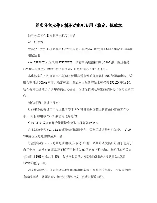
序流程很简单:1.上电初始化,H桥四个输入端均为高电平。
【启动电机】1.获得启动电机命令后先打开下桥2,输出80%占空比的PWM(因为本H桥驱动是低电平开启,80%PWM实际为100%-80%=20%)2.四到八个PWM周期延迟后打开上桥1(延迟不必控制得很严格)3.如设定转速应高于20%占空比PWM的转速,在半秒内逐渐增加下桥2PWM至设定的PWM(如设定电机应全速运转,则由最初80%占空比PWM逐渐降低至5%) 注:反转则为开上桥1-下桥2,过程相同不再复述。
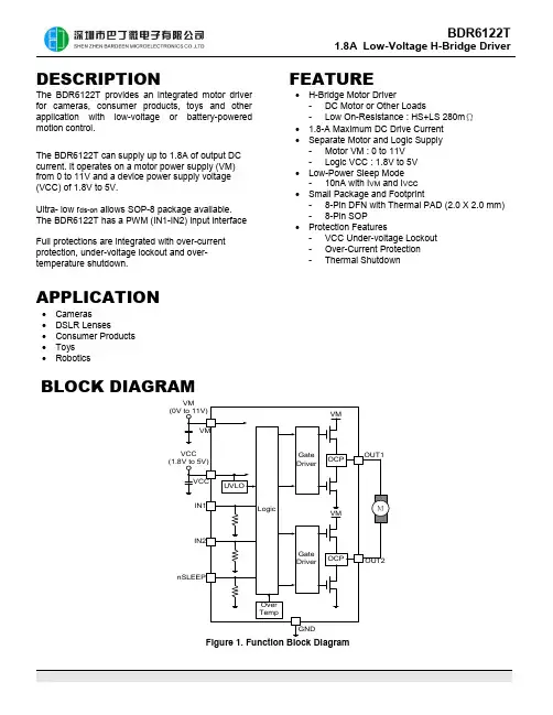
BDR6122T 1.8A Low-Voltage H-Bridge DriverDESCRIPTIONThe BDR6122T provides an integrated motor driver for cameras, consumer products, toys and other application with low-voltage or battery-powered motion control.The BDR6122T can supply up to 1.8A of output DC current. It operates on a motor power supply (VM) from 0 to 11V and a device power supply voltage (VCC) of 1.8V to 5V.Ultra- low r ds-on allows SOP-8 package available. The BDR6122T has a PWM (IN1-IN2) input interface Full protections are integrated with over-current protection, under-voltage lockout and over-temperature shutdown.APPLICATION∙Cameras∙DSLR Lenses∙Consumer Products∙Toys∙Robotics FEATURE∙H-Bridge Motor Driver- DC Motor or Other Loads- Low On-Resistance : HS+LS 280mΩ∙ 1.8-A Maximum DC Drive Current∙Separate Motor and Logic Supply- Motor VM : 0 to 11V- Logic VCC : 1.8V to 5V∙Low-Power Sleep Mode- 10nA with I VM and I VCC∙Small Package and Footprint- 8-Pin DFN with Thermal PAD (2.0 X 2.0 mm) - 8-Pin SOP∙Protection Features- VCC Under-voltage Lockout- Over-Current Protection- Thermal ShutdownBLOCK DIAGRAMFigure 1. Function Block DiagramAPPLICATION CIRCUITFigure 2. Schematic of Application*C3 is optional for better performance. Details are referred to at the chapter “Power Supply Recommendations”.PIN DESCRIPTIONVM OUT1OUT2GNDIN2IN1nSLEEP VCC DFN-8VM OUT1OUT2GNDIN2IN1nSLEEP VCC SOP-8FUNCTION DESCRIPTIONBRIDGE CONTROLThe BDR6122T is controlled using a PWM input interface, also called an IN-IN interface. Each output is controlled by aPROTECTION MANAGEMENTFUNCTIONAL MODESThe BDR6122T is active unless the nSLEEP pin is brought logic low. In sleep mode, the H-bridge FETs are disabledPOWER SUPPLY RECOMMENDATIONSHaving appropriate local bulk capacitance is an important factor in motor-drive system design. It is generally beneficial to have more bulk capacitance.The amount of local bulk capacitor needed depends on the following factors ,∙The highest current required by the motor system.∙The power-supply capacitance and ability to source current∙The amount of parasitic inductance between the power supply and motor system∙The acceptable voltage ripple∙The type of motor used (brushed dc, brushless dc, stepper)∙The motor braking methodThe inductance between the power supply and motor drive system limits the rate at which current can change from the power supply. If the local bulk capacitance is too small, the system responds to excessive current demands or dumps from the motor with a change in voltage. When adequate bulk capacitance is used, the motor voltage remains stable and high current can be quickly supplied.The voltage rating for bulk capacitors should be higher than the operating voltage, to provide margin for cases whenFigure 3. Motor Driver System with External Power SupplyPCB LAYOUTThe VM and VCC should be bypassed to GND using low-ESR ceramic capacitors with recommended value of 0.1µF. These capacitors should be placed as close to the VM and VCC as possible with a thick trace or ground plane connection to GND.0.1uF0.1uFELECTRICALCHARACTERISTICSTIMING REQUIREMENTST A =25℃IN1IN2OUT1OUT2OUTxTYPICAL OPERATING CHARACTERISTICSFigure 12. 50% Duty Cycle , Forward Direction Figure 13. 20% Duty Cycle , Forward Direction Figure 14. 50% Duty Cycle , Reverse Direction Figure 15. 20% Duty Cycle , Reverse DirectionPACKAGE INFORMATION 8-PIN, DFNNote:Refer to JEDEC MO-2298 PINS, SOP, 150MILNotes:1. Refer to JEDEC MS-012AA2. All dimensions are in millimeter。
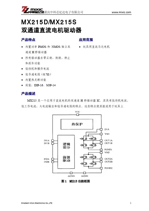
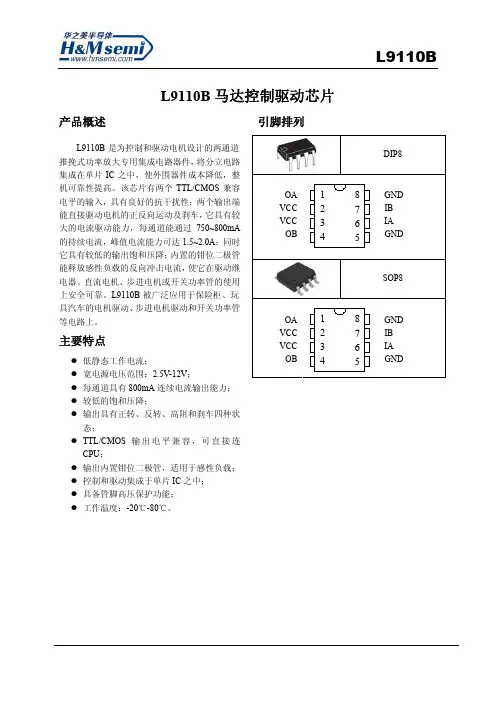
L9110B马达控制驱动芯片产品概述L9110B是为控制和驱动电机设计的两通道推挽式功率放大专用集成电路器件,将分立电路集成在单片IC之中,使外围器件成本降低,整机可靠性提高。
该芯片有两个TTL/CMOS兼容电平的输入,具有良好的抗干扰性;两个输出端能直接驱动电机的正反向运动及刹车,它具有较大的电流驱动能力,每通道能通过750~800mA 的持续电流,峰值电流能力可达1.5~2.0A;同时它具有较低的输出饱和压降;内置的钳位二极管能释放感性负载的反向冲击电流,使它在驱动继电器、直流电机、步进电机或开关功率管的使用上安全可靠。
L9110B被广泛应用于保险柜、玩具汽车的电机驱动、步进电机驱动和开关功率管等电路上。
主要特点z低静态工作电流;z宽电源电压范围:2.5V-12V;z每通道具有800mA连续电流输出能力;z较低的饱和压降;z输出具有正转、反转、高阻和刹车四种状态;z TTL/CMOS 输出电平兼容,可直接连CPU;z输出内置钳位二极管,适用于感性负载;z控制和驱动集成于单片IC之中;z具备管脚高压保护功能;z工作温度:-20℃-80℃。
引脚排列引脚功能序号符号功能描述序号符号功能描述1 OA A路输出管脚 5 GND 地线2 VCC 电源电压 6 IA A路输入管脚3 VCC 电源电压7 IB B路输入管脚4 OB B路输出管脚8 GND 地线电路功能框最大额定值参数说明符号范围单位最小值典型值最大值电源电压V CC 2.2 6 12 V 电流峰值I MAX — 1500 2000 mA输入高电平VH IN 2.5 5.0 12 V 输入低电平VL IN 0 0.5 0.7V允许电源消耗Pd max — — 800 mW操作温度T opr -30 25 85℃注意:如果器件运行条件超过上述各项最大额定值,可能对器件造成永久性损坏。
上述参数仅是运行条件的极大值,我们不建议器件在该规范范围外运行。
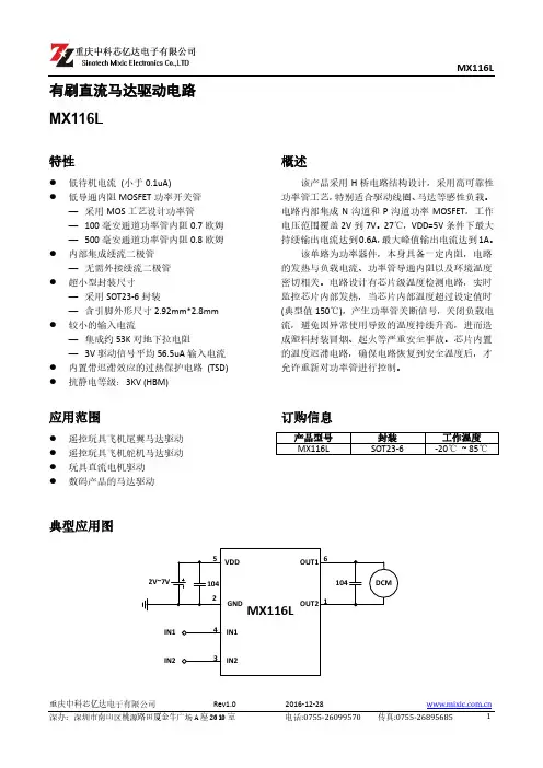
有刷直流马达驱动电路MX608 有刷直流马达驱动电路MX608概述该产品为电池供电的玩具、低压或者电池供电的运动控制应用提供了一种集成的有刷直流马达驱动解决方案。
电路内部集成了采用N沟和P沟功率MOSFET设计的H桥驱动电路,适合于驱动有刷直流马达或者驱动步进马达的一个绕组。
该电路具备较宽的工作电压范围(从2V到9.6V),最大持续输出电流达到0.8A,最大峰值输出电流达到1.5A。
该驱动电路内置过热保护电路。
通过驱动电路的负载电流远大于电路的最大持续电流时,受封装散热能力限制,电路内部芯片的结温将会迅速升高,一旦超过设定值(典型值150℃),内部电路将立即关断输出功率管,切断负载电流,避免温度持续升高造成塑料封装冒烟、起火等安全隐患。
内置的温度迟滞电路,确保电路恢复到安全温度后,才允许重新对电路进行控制。
特性●低待机电流(小于0.1uA);●低静态工作电流;●集成的H桥驱动电路;●内置防共态导通电路;●低导通内阻的功率MOSFET管;●内置带迟滞效应的过热保护电路(TSD);●抗静电等级:3KV (HBM)。
典型应用● 2-6节AA/AAA干电池供电的玩具马达驱动;● 2-6节镍-氢/镍-镉充电电池供电的玩具马达驱动;● 1-2节锂电池供电的马达驱动Sinotech Mixic Electronics Co.,LTD MX608引脚排列 引脚定义功能框图注:D A JAT A表示电路工作的环境温度,θJA为封装的热阻。
150℃表示电路的最高工作结温。
(2)、电路功耗的计算方法: P =I2*R其中P为电路功耗,I为持续输出电流,R为电路的导通内阻。
电路功耗P必须小于最大功耗P D(3)、人体模型,100pF电容通过1.5KΩ 电阻放电。
注:(1)、逻辑控制电源VCC与功率电源VDD内部完全独立,可分别供电。
当逻辑控制电源VCC掉电之后,电路将进入待机模式。
(2)、持续输出电流测试条件为:电路贴装在PCB上测试,SOP8封装的测试PCB板尺寸为22mm*18mm。
有刷直流马达驱动电路MX612 有刷直流马达驱动电路MX612概述该产品为电池供电的玩具、低压或者电池供电的运动控制应用提供了一种集成的有刷直流马达驱动解决方案。
电路内部集成了采用N沟和P沟功率MOSFET设计的H桥驱动电路,适合于驱动有刷直流马达或者驱动步进马达的一个绕组。
该电路具备较宽的工作电压范围(从2V到10V),最大持续输出电流达到1.2A,最大峰值输出电流达到2.5A。
该驱动电路内置过热保护电路。
通过驱动电路的负载电流远大于电路的最大持续电流时,受封装散热能力限制,电路内部芯片的结温将会迅速升高,一旦超过设定值(典型值150℃),内部电路将立即关断输出功率管,切断负载电流,避免温度持续升高造成塑料封装冒烟、起火等安全隐患。
内置的温度迟滞电路,确保电路恢复到安全温度后,才允许重新对电路进行控制。
特性●低待机电流(小于0.1uA);●低静态工作电流;●集成的H桥驱动电路;●内置防共态导通电路;●低导通内阻的功率MOSFET管;●内置带迟滞效应的过热保护电路(TSD);●抗静电等级:3KV (HBM)。
典型应用● 2-6节AA/AAA干电池供电的玩具马达驱动;● 2-6节镍-氢/镍-镉充电电池供电的玩具马达驱动;● 1-2节锂电池供电的马达驱动引脚排列 引脚定义功能框图注:D A JAT A表示电路工作的环境温度,θJA为封装的热阻。
150℃表示电路的最高工作结温。
(2)、电路功耗的计算方法: P =I2*R其中P为电路功耗,I为持续输出电流,R为电路的导通内阻。
电路功耗P必须小于最大功耗P D(3)、人体模型,100pF电容通过1.5KΩ 电阻放电。
注:(1)、逻辑控制电源VCC与功率电源VDD内部完全独立,可分别供电。
当逻辑控制电源VCC掉电之后,电路将进入待机模式。
(2)、持续输出电流测试条件为:电路贴装在PCB上测试,SOP8封装的测试PCB板尺寸为25mm*15mm。
电特性参数表测试原理图PMOS体二极管导通电压测试原理图NMOS体二极管导通电压测试原理图时间参数测试原理图时间参数定义MX612电特性曲线典型应用线路图图1 MX612典型应用线路图特别注意事项:图1中的功率电源VDD对地去耦电容(C1)容值应根据具体的应用调整,VDD电压越高,输出峰值电流越大,C1取值越大,但是电容C1的取值至少需要4.7uF。
在高压、大电流的应用条件下建议电容C1取值100uF。
逻辑电源VCC对地电容C2必须至少需要4.7uF,实际应用时不需要靠近芯片单独添加一个电容,可以与其它控制芯片(RX2、MCU)等共用。
如果VCC对地没有任何电容,当电路因过载进入过热保护模式后,电路可能会进入锁定状态。
进入锁定状态后,必须重新改变一次输入信号的状态,电路才能恢复正常。
只要VCC 对地有超过4.7uF电容,电路就不会出现锁定状态。
图2 2-6节电池供电玩具遥控车马达驱动应用线路图如图2所示的马达驱动应用线路图,其中转向轮驱动电流较小,可选择MX608作为驱动电路。
后轮马达驱动电流较大,可根据具体要求选择我公司其他产品,如MX612,MX615以及MX618。
图2中的VDD对地去耦电容应根据实际使用情况选择容值。
VDD电压越高,马达电流越大,电容容值越大。
电容必须大于4.7uF。
应用说明1、基本工作模式a)待机模式在待机模式下,INA=INB=L。
包括驱动功率管在内的所有内部电路都处于关断状态。
电路消耗极低极低的电流。
此时马达输出端OUTA和OUTB都为高阻状态。
b)正转模式正转模式的定义为:INA=H,INB=L,此时马达驱动端OUTA输出高电平,马达驱动端OUTB输出低电平时,马达驱动电流从OUTA流入马达,从OUTB流到地端,此时马达的转动定义为正转模式。
c)反转模式反转模式的定义为:INA=L,INB=H,此时马达驱动端OUTB输出高电平,马达驱动端OUTA输出低电平时,马达驱动电流从OUTB流入马达,从OUTA流到地端,此时马达的转动定义为反转模式。
d)刹车模式刹车模式的定义为:INA=H,INB=H,此时马达驱动端OUTA以及OUTB都输出低电平,马达内存储的能量将通过OUTA端NMOS管或者OUTB端NMOS快速释放,马达在短时间内就会停止转动。
注意在刹车模式下电路将消耗静态功耗。
e)PWM模式A当输入信号INA为PWM信号,INB=0或者INA=0,INB为PWM信号时,马达的转动速度将受PWM信号占空比的控制。
在这个模式下,马达驱动电路是在导通和待机模式之间切换,在待机模式下,所有功率管都处于关断状态,马达内部储存的能量只能通过功率MOSFET的体二极管缓慢释放。
注意:由于工作状态中存在高阻状态,因此马达的转速不能通过PWM信号的占空比精确控制。
如果PWM 信号的频率过高,马达会出现无法启动的情况。
PWM模式A信号波形示意图f)PWM模式B当输入信号INA为PWM信号,INB=1或者INA=1,INB为PWM信号时,马达的转动速度将受到PWM信号占空比的控制。
在这个模式下,马达驱动电路输出在导通和刹车模式之间,在刹车模式下马达存储的能量通过低边的NMOS管快速释放。
注意:由于工作状态中存在刹车状态,马达能量能快速释放,马达的转速能通过PWM信号的占空比精确控制,但必须注意如果PWM信号频率过低会导致马达因进入刹车模式而出现无法连续平滑转动的现象。
为减小电机噪音,建议PWM信号频率大于10KHz,小于50KHz。
PWM模式B信号波形示意图2、防共态导通电路在全桥驱动电路中,将半桥内的高边PMOS功率管和低边NMOS功率管同时导通的状态称为共态导通状态。
共态导通将出现一个电源至地的瞬态大电流,该电流会引起额外的功耗损失,极端情况下会烧毁电路。
通过内置死区时间,可避免共态导通。
典型的死区时间为300ns。
3、过热保护电路当驱动电路结温超过预设温度(典型值为150℃)时,TSD电路开始工作,此时控制电路强制关断所有输出功率管,驱动电路输出进入高阻状态。
TSD电路中设计了热迟滞,只有当电路的结温下降到预设温度(典型值130℃)时,电路返回正常工作状态。
4、驱动电路最大持续功耗该系列马达驱动电路内部均设计有过热保护电路,因此当驱动电路消耗的功耗过大时,电路将进入热关断模式,热关断状态下马达将无法正常工作。
驱动电路最大持续功耗的计算公式为:P M=(150℃-T A)/θJA其中150℃为热关断电路预设温度点,T A为电路工作的环境温度(℃),θJA为电路的结到环境的热阻(单位℃/W)。
注意:驱动电路的最大持续功耗与环境温度、封装形式以及散热设计等因素有关,与电路导通内阻并无直接关系。
5、驱动电路功耗马达驱动电路内部功率MOSFET的导通内阻是影响驱动电路功耗的主要因素。
驱动电路功耗的计算公式为:P D=I L2 *R ON其中I L表示马达驱动电路的输出电流,R ON表示功率MOSFET的导通内阻。
注意:功率MOSFET的导通内阻随着温度的升高而升高,在计算电路的最大持续输出电流以及功耗时必须考虑导通内阻的温度特性。
6、驱动电路最大持续输出电流根据驱动电路的最大持续功耗以及驱动电路功耗可计算出驱动电路的最大持续输出电流,计算公式为:其中的R ONT为考虑温度特性后的功率MOSFET导通内阻。
注意:驱动电路的最大持续输出电流与环境温度、封装形式、散热设计以及功率MOSFET的导通内阻等因素有关。
7、马达内阻选择上述分析表明,马达驱动电路的最大持续功耗有限。
如果马达驱动电路所驱动马达内阻极小,其堵转电流超过马达驱动电路所能承受的最大持续输出电流太多,则很容易导致马达驱动电路进入过热关断状态,玩具车在跑动或者反复前进、后退时将出现抖动的现象。
在马达驱动电路选型时,必须考虑马达的内阻。
特别注意事项1、电源与地反接将电路的电源与地线反接,将导致电路损坏,严重时会导致塑料封装冒烟。
可考虑在电路的电源端串联一个功率肖特基二极管至电池的正端,可防止由于电池接反引起的电路损坏。
功率肖特基二极管的最大持续电流能力必须大于马达堵转的持续电流,否则肖特基二极管会因为过热而损坏。
功率肖特基二极管的反向击穿电压必须大于最高电源电压,如果反向击穿电压过小,当电池反接时,会击穿肖特基二极管造成烧毁。
2、功率电源VDD对地去耦电容(C1)驱动电路要求添加的功率电源VDD对地去耦电容C1(参考应用线路图1)主要有两个作用:1)、吸收马达向电源释放的能量,稳定电源电压,避免电路因为过压而击穿;2)、在马达起动或者快速正转、反转切换的瞬间,马达需要瞬间大电流才能迅速启动。
由于电池的响应速度以及连接引线较长,往往不能立即输出瞬态大电流,此时需要依赖靠近马达驱动电路附近的储能电容释放出瞬态大电流。
根据电容的储能特性,电容容值越大,相同时间内的电压波动越小,因此在高压、大电流的应用条件下建议电容C1取值100uF,建议根据具体的应用选择电容值,但是该电容C1取值至少需要4.7uF。
3、静电防护电路的输入/输出端口采用了CMOS器件,对静电放电敏感。
虽然设计有静电防护电路,但在运输、包装、加工、储存过程中应该采取防静电措施,尤其是在加工过程中应重点考虑防静电。
4、输出对地短路、输出端短路在正常工作时,电路的高电平输出端与地线发生短路时或者OUTA与OUTB两端发生短路,电路内部将通过极大的电流,产生极大的功耗,触发电路内部的过热关断电路,从而保护电路不立即烧毁。
但由于过热保护电路只检测温度,并不检测通过电路的瞬态电流,输出对地短路时电流极大,容易造成电路损坏,使用时应避免发生输出对地短路。
测试时加入限流措施可避免发生类似损坏。
5、输出对电源短路在正常工作时,当电路的低电平输出端与电源发生短路时,电路将会被损坏。
6、马达堵转在正常工作时,当驱动电路的负载马达出现堵转的情况后,如果堵转电流超过驱动电路的最大持续电流,驱动电路将进入过热保护模式,防止电路损坏。
但如果堵转电流远大于最大峰值电流,电路较容易损坏。
7、峰值电流大大超过额定值在接近或超过最高工作电压且峰值电流大大超过绝对最大峰值电流时也会造成芯片烧毁。
MX612封装外形尺寸图SOP8:。