ad9642模数转换器中文资料
- 格式:pdf
- 大小:2.43 MB
- 文档页数:32

One Technology Way · P.O. Box 9106 · Norwood, MA 02062-9106 · Tel: 781.329.4700 · Fax: 781.461.3113 · EVALUATING THE AD9653/AD9253/AD9633 ANALOG-TO-DIGITAL CONVERTERSPrefaceThis user guide describes the AD9653, AD9253 and AD9633 evaluation boards, AD9653-125EBZ,AD9253-125EBZ and AD9633-125EBZ, which provide all of the support circuitry required to operate these parts in their various modes and configurations. The application software used to interface with the devices is also described.The AD9653AD9253 and AD9633 data sheets provide additional information and should be consulted when using the evaluation board. All documents and software tools are available at/hsadcevalboard. For additional information or questions, send an email to*******************************.Typical Measurement SetupFigure 1. Evaluation Board Connection—AD9653-125EBZ, AD9253-125EBZ or AD9633-125EBZ (on Left)and HSC-ADC-EVALCZ (on Right)FeaturesFull featured evaluation board for the AD9653/AD9253/AD9633qSPI interface for setup and controlqExternal, on-board oscillator, or AD9517 clocking optionqBalun/transformer or amplifier input drive optionqOn-board LDO regulator needing a single external 6 V, 2 A dc supplyqVisualAnalog® and SPI controller software interfacesqHelpful DocumentsAD9653, AD9253 or AD9633 data sheetqHigh speed ADC FIFO evaluation kit (HSC-ADC-EVALCZ)qAN-905 Application Note, VisualAnalog Converter Evaluation Tool Version 1.0 User ManualqAN-878 Application Note, High Speed ADC SPI Control SoftwareqAN-877 Application Note, Interfacing to High Speed ADCs via SPIqAN-835 Application Note, Understanding ADC Testing and EvaluationqDesign and Integration FilesSchematics, layout files, bill of materialsqEquipment NeededAnalog signal source and antialiasing filterqSample clock source (if not using the on-board oscillator)q2 switching power supplies (6.0 V, 2.5 A), CUI EPS060250UH-PHP-SZ providedqPC running Windows®qUSB 2.0 portqAD9653-125EBZ, AD9253-125EBZ or AD9633-125EBZ boardqHSC-ADC-EVALCZ FPGA-based data capture kitqGetting StartedThis section provides quick start procedures for using the AD9653-125EBZ, AD9253-125EBZ or AD9633-125EBZ board. Both the default and optional settings are described.Configuring the BoardBefore using the software for testing, configure the evaluation board as follows:1.Connect the evaluation board to the data capture board, as shown in Figure 1.2.Connect one 6 V, 2.5 A switching power supply (such as the CUI, Inc., EPS060250UH-PHP-SZ that is supplied) to the AD9653-125EBZ, AD9253-125EBZ or AD9633-125EBZ.3.Connect one 6 V, 2.5 A switching power supply (such as the supplied CUI EPS060250UH-PHP-SZ) to the HSC-ADC-EVALCZ board.Connect the HSC-ADC-EVALCZ board (J6) to the PC using a USB cable.4.5.On the ADC evaluation board, confirm that the jumpers are installed as shown in Figure 2 and Table 1.On the ADC evaluation board, use a clean signal generator with low phase noise to provide an6.input signal to the desired A and/or B channel(s). Use a 1 m, shielded, RG-58, 50 Ω coaxial cable to connect the signal generator. For best results, use a narrow-band, band-pass filter with 50 Ωterminations and an appropriate center frequency. (Analog Devices, Inc., uses TTE, Allen Avionics, and K&L band-pass filters.)Evaluation Board HardwareThe evaluation board provides the support circuitry required to operate the AD9653, AD9253 andAD9633 in their various modes and configurations. Figure 1 shows the typical bench characterization setup used to evaluate AC performance. It is critical that the signal sources used for the analog input and clock have very low phase noise (<1 ps rms jitter) to realize the optimum performance of the signal chain. Proper filtering of the analog input signal to remove harmonics and lower the integrated or broadband noise at the input is necessary to achieve the specified noise performance.See the Getting Started section to get started, and visit UG-328 Design Support for the complete schematics and layout diagrams. These diagrams demonstrate the routing and grounding techniques that should be applied at the system level when designing application boards using these converters.Power SuppliesThis evaluation board comes with a wall-mountable switching power supply that provides a 6 V, 2 A maximum output. Connect the supply to a 100 V ac to 240 V ac, 47 Hz to 63 Hz wall outlet. The output from the supply is provided through a 2.1 mm inner diameter jack that connects to the printed circuit board (PCB) at P101. The 6 V supply is fused and conditioned on the PCB before connecting to the low dropout linear regulators that supply the proper bias to each of the various sections on the board.The evaluation board can be powered in a nondefault condition using external bench power supplies. To do this, remove the E101, E102, E103 and E104 ferrite beads to disconnect the outputs from theon-board LDOs. This enables the user to bias each section of the board individually. Use P102 andP103 to connect a different supply for each section. A 1.8 V, 0.5 A supply is needed for 1.8V_AVDD and 1.8V_DRVDD. Although the power supply requirements are the same for AVDD and DRVDD, it is recommended that separate supplies be used for both analog and digital domains. The SPI and its level shifters and alternate clock options require a separate 3.3 V, 0.5 A analog supply.Two additional supplies, 5V_AVDD and 3V_AVDD, are used to bias the optional input path amplifiers and optional AD9517-3 clock chip. If used, these supplies should each have 0.5 A current capability. Input SignalsWhen connecting the ADC clock and analog source, use clean signal generators with low phase noise, such as the Rohde & Schwarz SMA, or HP 8644B signal generators or an equivalent. Use a 1 m shielded, RG-58, 50 Ω coaxial cable for connecting to the evaluation board. Enter the desired frequency and amplitude (see the Specifications section in the data sheet of the respective part). When connecting the analog input source, use of a multipole, narrow-band band-pass filter with 50 Ωterminations is recommended. Analog Devices uses band-pass filters from TTE and K&L Microwave, Inc. Connect the filters directly to the evaluation board.If an external clock source is used, it should also be supplied with a clean signal generator as previously specified. Analog Devices evaluation boards typically can accept ~2.8 V p-p or 13 dBm sine wave input for the clock.Output SignalsThe default setup uses the Analog Devices high speed converter evaluation platform (HSC-ADC-EVALCZ) for data capture. The serial LVDS outputs from the ADC are routed to ConnectorP1002 using 100 Ω differential traces. For more information on the data capture board and its optional settings, visit /hsadcevalboard.Jumper SettingsSet the jumper settings/link options on the evaluation board for the required operating modes before powering on the board. The functions of the jumpers are described in Table 1. Figure 2 shows the default jumper settings.Table 1. Jumper SettingsJumperDescriptionJ202This jumper selects between internal V REF and external V REF .To choose the internal 1 V reference, connect Pin 3 (DUT_SENSE) to Pin 5 (GND).To use the on-board ADR130 1 V reference, connect Pin 2 (DUT_SENSE) to Pin 1 (AVDD), and connect Pin 4 (DUT_VREF) to Pin 6 (EXT_REF).To apply a reference voltage from an external off-board source, connect Pin 2 (DUT_SENSE)to Pin 1 (AVDD) and apply the reference voltage to Pin 4 (DUT_VREF). The AD9653 canaccommodate reference voltages from 1.0 V to 1.3 V; the AD9253 and AD9633 referencevoltage is specified to be 1.0 V.J204Use this jumper to power down the ADC. Using the SPI, the PDWN pin can be configured to be STBY (standby).J302This jumper sets the ADC for SPI communications with the HSC-ADC-EVALCZ .Connect Pin 1 to Pin 2 for SDIO, Pin 4 to Pin 5 for SCLK, and Pin 8 to Pin 9 for CSB.J803This jumper enables the on-board crystal oscillator.Figure 2. Default Jumper Connections for AD9653-125EBZ /AD9253-125EBZ /AD9633-125EBZ Board Evaluation Board CircuitryThis section explains the default and optional settings or modes allowed on the AD9653-125EBZ ,AD9253-125EBZ and the AD9633-125EBZ boards.PowerPlug the switching power supply into a wall outlet rated at 100 V ac to 240 V ac, 47 Hz to 63 Hz. Connect the DC output connector to P101 on the evaluation board.Analog InputThe four channel inputs on the evaluation board are set up for a double balun-coupled analog input with a 50 Ω impedance. The default analog input configuration supports analog input frequencies of up to ~200 MHz.VREFThe default VREF configuration is to connect the SENSE pin to AGND for internal VREF operation. This is done by connecting Pin 3 to Pin 5 on Header J202. An external reference voltage can be provided to the AD9653, AD9253 and AD9633. Connecting Pin 2 to Pin 1 on Header J202 puts the ADC in a mode where it requires a reference voltage from an external source. The external on-board 1.0 V reference is provided by the ADR130. This external reference can be connected to the ADC by connecting Pin 4 to Pin 6 on Header J202. Alternatively, if an external off-board reference is desired, connect Pin 2 to Pin1 on Header J202 and apply the reference voltage directly to Pin 4 of Header J202. The AD9653 can accommodate reference voltages from 1.0 V to 1.3 V; the AD9253 and AD9633 reference voltage is specified to be 1.0 V.RBIASRBIAS has a default setting of 10 kΩ (R205) to ground and is used to set the ADC core bias current. Note that using a resistor value other than a 10 kΩ, 1% resistor for RBIAS may degrade the performance of the device.ClockThe default clock input circuit is derived from a simple transformer-coupled circuit using a high bandwidth 1:1 impedance ratio transformer (T801/T802) that adds a low amount of jitter to the clock path. The clock input is 50 Ω terminated and ac-coupled to handle single-ended sine wave types of inputs. The transformer converts the single-ended input to a differential signal that is clipped byCR801 before entering the ADC clock inputs. The AD9653, AD9253 and AD9633 ADCs are equipped with an internal 8:1 clock divider to facilitate usage with higher frequency clocks. When using the internal divider and a higher input clock frequency, remove CR801 to preserve the slew rate of the clock signal.The AD9653-125EBZ, AD9253-125EBZ and AD9633-125EBZ boards are set up to be clocked through the transformer-coupled input network from the crystal oscillator, Y801. This oscillator is a low phase noise oscillator from Valpey Fisher (VFAC3-BHL-125MHz). If a different clock source is desired, remove C810 (optional) and Jumper J803 to disable the oscillator from running and connect the external clock source to the SMA connector, J802 (labeled CLK+).PDWNTo enable the power-down feature, add a shorting jumper across J204 at Pin 1 and Pin 2 to connect the PDWN pin to DRVDD.Modes of OperationStandalone (PIN) ModeThe AD9653/AD9253/AD9633 ADCs can operate in pin mode if there is no need to program and change the default modes of operation via the SPI. For applications that do not require SPI mode operation, the CSB pin is tied to AVDD, and the SDIO/OLM pin controls the output lane mode. Table 2 and Table 3 specify the settings for pin mode operation.Table 2. Output Lane Mode (OLM) Pin SettingsOLM Pin Voltage Output ModeAVDD (Default)Two-lane. 1× frame, 16-bit serial outputGND One-lane. 1× frame, 16-bit serial outputTable 3. Digital Test Pattern (DTP) Pin SettingsSeected DTP Output Mode Resulting D0±x and D1±xNormal Operation10 kΩ to AGND Normal operationDTP AVDD1000 0000 0000 0000Additional information on the lane modes is provided in the AD9653, AD9253 and AD9633 data sheets.Default ModeTo operate the device under test (DUT) using the SPI, follow the jumper settings for J302 as shown in Table 1.How To Use The Software For TestingSetting up the ADC Data CaptureAfter configuring the board, set up the ADC data capture using the following steps:1.Open VisualAnalog on the connected PC. The appropriate part type should be listed in the status bar of the VisualAnalog – New Canvas window. Select the template that corresponds to the type of testing to be performed (see Figure 3, where the AD9253 is shown as an example).Figure 3. VisualAnalog, New Canvas Window2.After the template is selected, a message appears asking if the default configuration can be used to program the FPGA (see Figure 4). Click Yes, and the window closes.Figure 4. VisualAnalog Default Configuration Message3.To change features to settings other than the default settings, click the Expand Display button,located on the bottom right corner of the window (see Figure 5), to see what is shown in Figure 6. 4.Change the features and capture settings by consulting the detailed instructions in the AN-905 Application Note, VisualAnalog Converter Evaluation Tool Version 1.0 User Manual. After the changes are made to the capture settings, click the Collapse Display button.Figure 5. VisualAnalog Window Toolbar, Collapsed DisplayFigure 6. VisualAnalog, Main Window Expanded DisplayEvaluation And TestSetting up the SPI Controller SoftwareAfter the ADC data capture board setup is complete, set up the SPI controller software using the following procedure:1.Open the SPI controller software by going to the Start menu or by double-clicking theSPIController software desktop icon. If prompted for a configuration file, select the appropriate one. If not, check the title bar of the window to determine which configuration is loaded. Ifnecessary, choose Cfg Open from the File menu and select the appropriate file based on your part type. Note that the CHIP ID(1) box should be filled to indicate whether the correct SPI controller configuration file is loaded (see Figure 7).Figure 7. SPI Controller, CHIP ID(1) BoxClick the New DUT button in the SPIController window (see Figure 8)2.Figure 8. SPI Controller, New DUT Button3.In the ADCBase 0 tab of the SPIController window, find the CLOCK DIVIDE(B) box (see Figure9). If using the clock divider, use the drop-down box to select the correct clock divide ratio, ifnecessary. For additional information, refer to the data sheet, the AN-878 Application Note, High Speed ADC SPI Control Software, and the AN-877 Application Note, Interfacing to High Speed ADCsvia SPI.Figure 9. SPI Controller, CLOCK DIVIDE(B) Box4.Note that other settings can be changed on the ADCBase 0 tab (see Figure 9) and the ADC A, ADC B, ADC C, and ADC D tabs (see Figure 10) to set up the part in the desired mode. TheADCBase 0 tab settings affect the entire part, whereas the settings on the ADC A, ADC B, ADC C, and ADC D tabs affect the selected channel only. See the appropriate part data sheet, the AN-878 Application Note, High Speed ADC SPI Control Software, and the AN-877 Application Note,Interfacing to High Speed ADCs via SPI, for additional information on the available settings.Figure 10. SPI Controller, Example ADC A Page5.Click the Run button in the VisualAnalog toolbar (see Figure 11).Figure 11. Run Button (Encircled in Red) in VisualAnalog Toolbar, Collapsed DisplayAdjusting the Amplitude of the Input SignalThe next step is to adjust the amplitude of the input signal for each channel as follows:Adjust the amplitude of the input signal so that the fundamental is at the desired level. Examine 1.the Fund Power reading in the left panel of the VisualAnalog Graph - AD9253 FFT window(see Figure 12).Figure 12. Graph Window of VisualAnalogRepeat this procedure for Channel B, Channel C, and Channel D.2.3.Click the disk icon within the VisualAnalog Graph - AD9253 FFT window to save theperformance plot data as a .csv formatted file. See Figure 13 for an example.Figure 13. Typical FFT, AD9253Troubleshooting TipsIf the FFT plot appears abnormal, do the following:If you see an abnormal noise floor, go to the ADCBase0 tab of the SPIController window andqtoggle the Chip Power Mode in MODES(8) from Chip Run to Reset and back.If you see a normal noise floor when you disconnect the signal generator from the analog input, be qsure that you are not overdriving the ADC. Reduce the input level if necessary.In VisualAnalog, click the Settings icon in the Input Formatter block. Check that NumberqFormat is set to the correct encoding (twos complement by default). Repeat for the other channels.If the FFT appears normal but the performance is poor, check the following:Make sure that an appropriate filter is used on the analog input.qMake sure that the signal generators for the clock and the analog input are clean (low phase noise). qChange the analog input frequency slightly if noncoherent sampling is being used.qMake sure that the SPI configuration file matches the product being evaluated.qIf the FFT window remains blank after Run in VisualAnalog (see Figure 11) is clicked, do the following:Make sure that the evaluation board is securely connected to the HSC-ADC-EVALCZ board.qMake sure that the FPGA has been programmed by verifying that the DONE LED is illuminated onqthe HSC-ADC-EVALCZ board. If this LED is not illuminated, make sure that the U4 switch on the board is in the correct position for USB CONFIG.Make sure that the correct FPGA program was installed by clicking the Settings icon in the ADCqData Capture block in VisualAnalog. Then select the FPGA tab and verify that the proper FPGA bin file is selected for the part.If VisualAnalog indicates that the FIFO Capture timed out, do the following:Make sure that all power and USB connections are secure.qProbe the DCO signal at P1002 (Pin A10 and/or Pin B10) on the evaluation board, and confirm that a qclock signal is present at the ADC sampling rate.© Analog Devices, Inc. All rights reserved. Trademarks andregistered trademarks are the property of their respective 。

DATASHEET12-Ch a n n e l1:2M UX/DE M UX IC9642 Revision V0.1COPYRIGHT©2020 Shenzhen IcSpring Technology Co., Ltd all rights reserved. No part of this document may be reproduced, transmitted, transcribed, stored in a retrieval system, or translated into any language in any form or by any means without the written permission of Shenzhen IcSpring Technology Co., Ltd.DISCLAIMERIcSpring Technology Co. Ltd provides this document “as is”, without warranty of any kind, neither expressed nor implied, including, but not limited to, the particular purpose. IcSpring Technology Co. reserves the right to make changes at any time without notice to improve and supply the best possible product and is not responsible and does not assume any liability for misapplication or use outside the limits specified in this document. This document could include technical inaccuracies or typographical errors.TRADEMARKSIcSpring is a trademark, of Shenzhen IcSpring Technology Co., Ltd. Other names mentioned in this document trademarks/registered trademarks of their respective owners.USING THIS DOCUMENTThis document is intended for the hardware and software engineer’s general information on the IcSpring IC9642 12-Channel 1:2 MUX/DEMUX IC.Though every effort has been made to ensure that this document is current and accurate, more information may have become available subsequent to the production of this guide. In that event, please contact your IcSpring representative for additional information that may help in the development process.REVISION HISTORYTable of Contents1. Introduction (4)1.1 Description (4)2. Features (5)2.1 General System Features (5)2.2 Applications (5)3. Pin Assignment (6)3.1 Pin Assignment Diagram (6)3.2 Pin Descriptions (7)4. System Architecture and Reference Design (9)4.1 Functional Block Diagram (9)4.2 Device Functional Modes (9)4.3 HDMI Application Schematic (10)5. Electrical Characteristics (11)5.1 Absolute Maximum Ratings (11)5.2 DC Characteristics (11)5.3 Switching Characteristics (12)5.4 HDMI Eye Pattern (12)6. Mechanical Information (13)7. Application Circuits (14)7.1 Circuit (15)7.2 Layout Guidelines (15)7.3 Layout Example (16)1.Introduction1.1 DescriptionThe IC9642 is a 12 channel 1:2 or 2:1 bidirectional multiplexer/demultiplexer. The IC9642 operates 3.3V and offers low resistance to achieve a typical bandwidth of up to 6.9 GHz. The device provides the high bandwidth necessary for HDMI 2.0 applications. The IC9642 offers a power down mode to operate minimal power consumption.2.Features2.1. General System Features• 2:1 multiplexer• 1:2 demultiplexer• VCC: 3.3V• I/O: 0 ~ 5V• Support HDMI 2.0 up to 4K 60Hz• ESD Performance– 2KV Human Body Model• 42-pin WQFN Package (9 mm x 3.5 mm, 0.5 mm pitch)2.2 Applications• General Purpose DVI 1.0•DisplayPort•TMDS•LVDS•High-Speed•HDMI Signal Switching3. Pin Assignment3.1 Pin AssignmentFigure 3.1 Pin Assignment Diagram3.2 Pin Descriptions4. System Functional Descriptions 4.1 Functional Block DiagramFigure 4.1IC9642 Block Diagram4.2 Device Functional ModesFigure 4.2 Functional Table4.3 HDMI Application Schematic5. Electrical Characteristics5.1 Absolute Maximum RatingsTable 5.1. Absolute Maximum Ratings5.2 DC CharacteristicsTable 5.2 General DC Characteristics6. Mechanical InformationFigure 6.1 Mechanical Information Diagram。

ADI公司的高速模数转换器(高速ADC)提供市场上最佳的性能和最高的ADC采样速度。
该系列产品包括高中频ADC (10MSPS -125MSPback to top Integrated ReceiverPart#ResolutionThroughput Rate# ADCInputsFPBW(typ)VsupplyPositive(min)VsupplyPositive(max)PowerDissipation (typ)OperatingTempRangeAD667711250 MSPS1 1 GHz 1.7 1.9500 mW-40 to +85 AD667311250 MSPS2400 MHz----AD6657AReferenceCircuitAvailable11200 MSPS4800 MHz 1.7 1.9--40 to +85AD667211250 MSPS1350 MHz 1.7 1.9423 mW-40 to +85 AD664914250 MSPS2 1 GHz 1.7 1.9 1.16 W-40 to +85 AD66591280 MSPS2700 MHz 1.7 1.9264 mW-25 to +85 AD7626ReferenceCircuitAvailable1610 MSPS195 MHz 4.75 5.25150 mW-40 to +85AD665711200 MSPS4800 MHz 1.7 1.9 1.3 W-40 to +85 AD664211200 MSPS2800 MHz 1.7 1.9620 mW-40 to +85 AD7400AReference Circuit Available 1610 MSPS1- 4.5 5.595 mW-40 to+125AD74001610 MSPS1- 4.5 5.590 mW-40 to+105AD665414-1270 MHz-- 2.5 W-25 to +85 AD665016 1 MSPS2- 3.15 3.45 2.1 W-25 to +85 AD66001120 MSPS2450 MHz 4.75 5.25976 mW-40 to +85 AD92201210 MSPS160 MHz 4.75 5.25310 mW-40 to +85 back to topLow-IFPart#DevicePrimaryFunctionResolutionThroughput Rate# ADCInputsFPBW(typ)VsupplyPositive(min)VsupplyPositive(max)PowerDissipation (typ)AD9653Low-IF16125 MSPS4650 MHz 1.7 1.9673 mW AD9637-40Low-IF1240 MSPS8650 MHz 1.7 1.9347 mW AD9633-105Low-IF12105 MSPS4650 MHz 1.7 1.9385 mW AD9257-40Low-IF1440 MSPS8650 MHz 1.7 1.9360 mWback to top Wide BandPart#ResolutionThroughput Rate# ADCInputsFPBW(typ)VsupplyPositive(min)VsupplyPositive(max)PowerDissipation (typ)OperatingTempRangeAD94848500 MSPS1 1 GHz 1.75 1.9670 mW-AD9434-370Reference CircuitAvailable12370 MSPS1 1 GHz 1.75 1.9595 mW-40 to +85AD6641-50012500 MSPS1 1 GHz 1.82695 mW-40 to +85AD74001610 MSPS1- 4.5 5.590 mW-40 to+105AD9434-500Reference CircuitAvailable12500 MSPS1 1 GHz 1.75 1.9660 mW-40 to +85品包括高中频ADC (10MSPS -125MSPS)、集成接收机的低中频ADC (125MSPS – 1GSPS)和宽带ADC (>1GSPS),提供面向所有高速转换应用的解决Operating Temp Range US Price 1000 to 4999-40 to +85$38.40 -40 to +85$72.49 -40 to +85$38.40 -40 to +85$20.35 -40 to +85$11.25 -40 to +85$109.74 -40 to +85$38.50 -40 to +85$135.15 -40 to +85--40 to +85$36.43 -40 to +85$114.92 -40 to +85$98.52 -40 to +85$53.00 -40 to +85$41.65 -40 to +85$131.57 -40 to +85$109.74 -40 to +85$69.65 -40 to +85$57.80 -40 to +85$35.25-40 to +85$29.25 -40 to +85$66.50 -40 to +85$55.50 -40 to +85$18.00US Price1000 to4999$44.20$74.80$111.35$44.20$83.30-$34.95$129.71$70.13$3.05$3.15$78.75$20.64$38.96$6.12Operating Temp Range US Price 1000 to 4999-40 to +85$250.00 -40 to+125$40.46 -40 to +85$57.80 -40 to +85$46.67-40 to +85$99.45-40 to +85$42.29-40 to +85$36.00 -40 to +85$25.00-40 to +85$100.30 -40 to +85$28.00 -40 to +85$49.00 -40 to +85$12.00 -40 to +85$5.25 -40 to +85$56.67 -40 to +85$45.00 -40 to +85--40 to +85$18.50-40 to +85$5.00 -40 to +85$119.00 -40 to +85$76.50 -40 to +85$101.15 -40 to +85$34.91 -40 to +85$34.91 -40 to +85$32.38 -40 to +85$62.24 -40 to +85$32.38-40 to +85$55.66 -40 to +85$54.65-40 to +85$40.48 -40 to +85$28.34 -40 to +85$57.35-40 to +85$14.17 -40 to +85$45.54 -40 to +85$65.78-40 to +85$40.43 -40 to +85$23.02 -40 to +85$20.24 -40 to +85$14.17 -40 to +85$57.35 -40 to +85$41.49 -40 to +85--40 to +85$34.41 -40 to +85$18.98-40 to +85$16.19 -40 to +85$32.69 -40 to +85$10.52-40 to +85$11.39-40 to +85$18.20 -40 to +85$16.70-40 to +85$7.59 -40 to +85$18.86 -40 to +85$11.13 -40 to +85$39.97-40 to +85$32.84 -40 to +85$17.33 -40 to +85$7.08-40 to +85$53.10 -40 to +85$10.83 -40 to +85$20.50 -25 to +85$32.28 -40 to +85$32.84 -40 to +85$3.80 -40 to +85$10.63 -40 to +85$18.51 -25 to +85$5.57-40 to +85$14.47 -40 to +85$12.19 -40 to +85$6.96 -40 to +85$3.91 -40 to +85$5.01 -40 to +85$37.61 -40 to +85$2.18 -40 to +85$18.37 -40 to +85$2.53 -40 to +85$13.23-40 to +85$2.56 -40 to +85$3.65 -40 to +85$25.00 -40 to +85$23.35 -40 to +85$15.13 -40 to +85$51.25 -40 to +85$37.95-40 to +85$74.38-40 to$56.95 +125-40 to +85$44.20 -40 to +85$68.51 -40 to +85$16.70 -40 to +85$12.08 -40 to +85$6.85 -40 to +85$25.35 -40 to +85$48.55 -40 to +85$41.75 -40 to +85$59.46 -40 to +85$42.00 -40 to +85$4.50 -40 to +85$4.17 -40 to +85$3.75 -40 to +85$3.50 -40 to +85$37.85 -40 to +85$20.19 -40 to +85$11.40 -40 to +85$119.85 -40 to +85$48.91-40 to +85$55.66 -40 to +85$34.51 -40 to +85$26.44 -40 to +85$55.66 -40 to +85$5.87 -40 to +85$3.44 -25 to +85$3.04 -25 to +85$2.53 -40 to +85$84.09 -40 to +85--40 to +85$59.50 -40 to +85$101.00 -40 to +85$136.00 -40 to +85$48.33 -40 to +85$43.33 -40 to +85$35.00 -40 to +85$48.33 -40 to +85$65.00 -40 to +85$55.25 -40 to +85$93.50-40 to +85$33.00 -40 to +85$59.93-55 to$170.00 +125-40 to +85$116.45 -40 to +85$37.50 -40 to +85$35.00 -40 to +85$23.89 -40 to +85$29.85 -40 to +85$24.04 -40 to +85$25.30 -40 to +85$49.08 -40 to +85$25.15 -40 to +85$169.15 -40 to +85$121.55 -40 to +85$18.22 -40 to +85$12.14 -40 to +85--40 to +85$8.00-40 to +85$12.14-40 to +85$7.99-40 to +85$16.90-40 to +85--40 to +85--40 to +85$44.53 -40 to +85$27.73 -40 to +85$55.51 -40 to +85$48.58 -40 to +85$16.19 -40 to +85$13.52 -40 to +85$11.90 -40 to +85$9.11 -40 to +85--40 to +85$7.59 -40 to +85$6.78 -40 to +85$5.06 -40 to +85$8.45 -40 to +85$6.33 -40 to +85$32.38 -40 to +85$46.55 -40 to +85$39.47 -40 to +85--40 to +85$7.50 -40 to +85$7.20-40 to +85$2.89 -40 to +85$21.22 -40 to +85--25 to +85$43.41US Price 1000 to 4999Device Primary Function$36.00Wide Band $85.00Wide Band-Wide Band $3.15-$124.95Wide BandS),提供面向所有高速转换应用的解决方案。
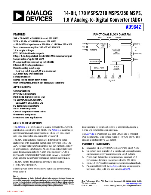
14-Bit, 170 MSPS/210 MSPS/250 MSPS,1.8 V Analog-to-Digital Converter (ADC)AD9642 Rev. 0Information furnished by Analog Devices is believed to be accurate and reliable. However, noresponsibility is assumed by Analog Devices for its use, nor for any infringements of patents or other rights of third parties that may result from its use. Specifications subject to change without notice. No license is granted by implication or otherwise under any patent or patent rights of Analog Devices. T rademarks and registered trademarks are the property of their respective owners. One Technology Way, P.O. Box 9106, Norwood, MA 02062-9106, U.S.A. Tel: 781.329.4700 Fax: 781.461.3113 ©2011 Analog Devices, Inc. All rights reserved.FEATURESSNR = 71.0 dBFS at 185 MHz A IN and 250 MSPSSFDR = 83 dBc at 185 MHz A IN and 250 MSPS−152.0 dBFS/Hz input noise at 200 MHz, −1 dBFS A IN, 250 MSPS Total power consumption: 390 mW at 250 MSPS1.8 V supply voltagesLVDS (ANSI-644 levels) outputsInteger 1-to-8 input clock divider (625 MHz maximum input) Sample rates of up to 250 MSPSIF sampling frequencies of up to 350 MHzInternal ADC voltage referenceFlexible analog input range1.4 V p-p to2.0 V p-p (1.75 V p-p nominal)ADC clock duty cycle stabilizerSerial port controlEnergy saving power-down modesUser-configurable, built-in self-test (BIST) capability APPLICATIONSCommunicationsDiversity radio systemsMultimode digital receivers (3G)TD-SCDMA, WiMAX, WCDMA,CDMA2000, GSM, EDGE, LTEI/Q demodulation systemsSmart antenna systemsGeneral-purpose software radiosUltrasound equipmentBroadband data applications FUNCTIONAL BLOCK DIAGRAM9995-1Figure 1.GENERAL DESCRIPTIONThe AD9642 is a 14-bit analog-to-digital converter (ADC) with sampling speeds of up to 250 MSPS. The AD9642 is designed to support communications applications, where low cost, small size, wide bandwidth, and versatility are desired.The ADC core features a multistage, differential pipelined architecture with integrated output error correction logic. The ADC features wide bandwidth inputs that can support a variety of user-selectable input ranges. An integrated voltage reference eases design considerations. A duty cycle stabilizer (DCS) is provided to compensate for variations in the ADC clock duty cycle, allowing the converter to maintain excellent performance. The ADC output data is routed directly to the external14-bit LVDS output port.Flexible power-down options allow significant power savings, when desired. Programming for setup and control is accomplished using a3-wire SPI-compatible serial interface.The AD9642 is available in a 32-lead LFCSP and is specified over the industrial temperature range of −40°C to +85°C. This product is protected by a U.S. patent.PRODUCT HIGHLIGHTS1.Integrated 14-bit, 170 MSPS/210 MSPS/250 MSPS ADC.2.Operation from a single 1.8 V supply and a separate digitaloutput driver supply accommodating LVDS outputs.3.Proprietary differential input maintains excellent SNRperformance for input frequencies of up to 350 MHz.4.3-pin, 1.8 V SPI port for register programming and readback.5.Pin compatibility with the AD9634, allowing a simple migra-tion from 14 bits to 12 bits, and with the AD6672.AD9642Rev. 0 | Page 2 of 28TABLE OF CONTENTSFeatures..............................................................................................1 Applications.......................................................................................1 Functional Block Diagram..............................................................1 General Description.........................................................................1 Product Highlights...........................................................................1 Revision History...............................................................................2 Specifications.....................................................................................3 ADC DC Specifications...............................................................3 ADC AC Specifications...............................................................4 Digital Specifications...................................................................5 Switching Specifications..............................................................6 Timing Specifications..................................................................7 Absolute Maximum Ratings............................................................8 Thermal Characteristics..............................................................8 ESD Caution..................................................................................8 Pin Configurations and Function Descriptions...........................9 Typical Performance Characteristics...........................................10 Equivalent Circuits.........................................................................16 Theory of Operation......................................................................17 ADC Architecture......................................................................17 Analog Input Considerations...................................................17 Voltage Reference.......................................................................19 Clock Input Considerations......................................................19 Power Dissipation and Standby Mode....................................20 Digital Outputs...........................................................................20 Serial Port Interface (SPI)..............................................................22 Configuration Using the SPI.....................................................22 Hardware Interface.....................................................................22 SPI Accessible Features..............................................................23 Memory Map..................................................................................24 Reading the Memory Map Register Table...............................24 Memory Map Register Table.....................................................25 Applications Information..............................................................27 Design Guidelines......................................................................27 Outline Dimensions.......................................................................28 Ordering Guide.. (28)REVISION HISTORY7/11—Revision 0: Initial VersionAD9642Rev. 0 | Page 3 of 28SPECIFICATIONSADC DC SPECIFICATIONSAVDD = 1.8 V , DRVDD = 1.8 V , maximum sample rate, VIN = −1.0 dBFS differential input, 1.75 V p-p full-scale input range, DCS enabled, unless otherwise noted. Table 1.AD9642-170 AD9642-210 AD9642-250Parameter Temperature Min Typ Max Min Typ Max Min Typ Max Unit RESOLUTION Full 14 14 14 Bits ACCURACY No Missing Codes Full Guaranteed Guaranteed Guaranteed Offset Error Full ±11 ±11 ±10 mV Gain Error Full +2/−11 +3.5/−8 +3/−7 %FSR Differential Nonlinearity (DNL) Full ±0.5 ±0.55 ±0.6 LSB 25°C ±0.3 ±0.3 ±0.32 LSBIntegral Nonlinearity (INL)1Full ±1.3 ±2.0 ±2.5 LSB 25°C ±0.6 ±0.75 ±1.0 LSB TEMPERATURE DRIFT Offset Error Full ±7 ±7 ±7 ppm/°C Gain Error Full ±52 ±105 ±75 ppm/°C INPUT REFERRED NOISE VREF = 1.0 V 25°C 0.83 0.85 0.85 LSBrmsANALOG INPUT Input Span Full 1.75 1.75 1.75 V p-pInput Capacitance 2Full 2.5 2.5 2.5 pF Input Resistance 3 Full 20 20 20 kΩ Input Common-Mode Voltage Full 0.9 0.9 0.9 V POWER SUPPLIES Supply Voltage AVDD Full 1.7 1.8 1.9 1.7 1.8 1.9 1.7 1.8 1.9 V DRVDD Full 1.7 1.8 1.9 1.7 1.8 1.9 1.7 1.8 1.9 V Supply CurrentI AVDD 1Full 123 136 129 139 136 146 mA I DRVDD 1 Full 50 64 56 67 64 69 mA POWER CONSUMPTION Sine Wave Input (DRVDD = 1.8 V) Full 311 360 333 371 360 387 mWStandby Power 4Full 50 50 50 mW Power-Down Power Full 5 5 5 mW1 Measured with a low input frequency, full-scale sine wave.2Input capacitance refers to the effective capacitance between one differential input pin and its complement. 3Input resistance refers to the effective resistance between one differential input pin and its complement. 4Standby power is measured with a dc input and the CLK pin inactive (that is, set to AVDD or AGND).AD9642Rev. 0 | Page 4 of 28ADC AC SPECIFICATIONSAVDD = 1.8 V , DRVDD = 1.8 V , maximum sample rate, VIN = −1.0 dBFS differential input, 1.75 V p-p full-scale input range, unless otherwise noted. Table 2.AD9642-170 AD9642-210 AD9642-250 Parameter 1 Temperature Min Typ Max Min Typ Max Min Typ Max Unit SIGNAL-TO-NOISE RATIO (SNR) f IN = 30 M H z 25°C 72.5 72.4 72.2 dBFS f IN = 90 M H z 25°C 72.2 72.2 72.0 dBFS Full 70.7 70.0 dBFS f IN = 140 M H z 25°C 71.8 71.6 71.8 dBFS f IN = 185 M H z 25°C 71.2 71.5 71.4 dBFS Full 68.6 dBFS f IN = 220 M H z 25°C 70.7 71.0 70.9 dBFS SIGNAL-TO-NOISE AND DISTORTION (SINAD) f IN = 30 M H z 25°C 71.5 71.5 71.2 dBFS f IN = 90 M H z 25°C 71.3 71.3 71.0 dBFS Full 69.6 68.7 dBFS f IN = 140 M H z 25°C 70.8 70.6 70.9 dBFS f IN = 185 M H z 25°C 70.3 70.5 70.4 dBFS Full 67.5 dBFS f IN = 220 M H z 25°C 69.7 70.1 70.0 dBFS EFFECTIVE NUMBER OF BITS (ENOB) f IN = 30 M H z 25°C 11.6 11.6 11.5 Bits f IN = 90 M H z 25°C 11.6 11.6 11.5 Bits f IN = 140 M H z 25°C 11.5 11.4 11.5 Bits f IN = 185 M H z 25°C 11.4 11.4 11.4 Bits f IN = 220 M H z 25°C 11.3 11.3 11.3 Bits WORST SECOND OR T H IRD H ARMONIC f IN = 30 M H z 25°C −96 −96 −90 dBc f IN = 90 M H z 25°C −95 −92 −89 dBc Full −82 −79 dBc f IN = 140 M H z 25°C −97 −94 −90 dBc f IN = 185 M H z 25°C −86 −95 −86 dBc Full −80 dBc f IN = 220 M H z 25°C −84 −84 −86 dBcSPURIOUS-FREE DYNAMIC RANGE (SFDR)f IN = 30 M H z 25°C 96 96 90 dBc f IN = 90 M H z 25°C 95 92 89 dBc Full 82 79 dBc f IN = 140 M H z 25°C 97 94 90 dBc f IN = 185 M H z 25°C 86 95 86 dBc Full 80 dBc f IN = 220 M H z 25°C 84 84 86 dBc WORST OT H ER (H ARMONIC OR SPUR) f IN = 30 M H z 25°C −99 −98 −95 dBc f IN = 90 M H z 25°C −95 −97 −98 dBc Full −87 −81 dBc f IN = 140 M H z 25°C −98 −96 −97 dBc f IN = 185 M H z 25°C −96 −97 −96 dBc Full −81 dBc f IN = 220 M H z 25°C −97 −94 −95 dBc TWO-TONE SFDR f IN = 184.1 MHz, 187.1 MHz (−7 dBFS) 25°C 87 88 88 dBcAD9642Rev. 0 | Page 5 of 28AD9642-170 AD9642-210 AD9642-250Parameter 1Temperature Min Typ Max Min Typ Max Min Typ Max UnitFULL POWER BANDWIDTH 225°C 350 350 350 M H z NOISE BANDWIDTH 3 25°C 1000 1000 1000 M H z1 See the AN-835 Application Note , Understanding High Speed ADC Testing and Evaluation , for a complete set of definitions. 2Full power bandwidth is the bandwidth of operation where typical ADC performance can be achieved. 3Noise bandwidth is the −3 dB bandwidth for the ADC inputs across which noise may enter the ADC and is not attenuated internally.DIGITAL SPECIFICATIONSAVDD = 1.8 V , DRVDD = 1.8 V , maximum sample rate, VIN = −1.0 dBFS differential input, 1.0 V internal reference, DCS enabled, unless otherwise noted. Table 3.ParameterTemperature Min Typ Max Unit DIFFERENTIAL CLOCK INPUTS (CLK+, CLK−)Logic ComplianceCMOS/LVDS/LVPECLInternal Common-Mode Bias Full 0.9 V Differential Input Voltage Full 0.3 3.6 V p-p Input Voltage RangeFull AGND AVDD V Input Common-Mode Range Full 0.9 1.4 V High Level Input Current Full 10 22 μA Low Level Input Current Full −22 −10 μA Input Capacitance Full 4 pF Input Resistance Full 12 15 18 kΩ LOGIC INPUT (CSB)1High Level Input Voltage Full 1.22 2.1 V Low Level Input Voltage Full 0 0.6 V High Level Input Current Full 50 71 μA Low Level Input Current Full −5 +5 μA Input Resistance Full 26 kΩ Input Capacitance Full 2 pF LOGIC INPUT (SCLK)2High Level Input Voltage Full 1.22 2.1 V Low Level Input Voltage Full 0 0.6 V High Level Input Current Full 45 70 μA Low Level Input Current Full −5 +5 μA Input Resistance Full 26 kΩ Input Capacitance Full 2 pF LOGIC INPUTS (SDIO)1High Level Input Voltage Full 1.22 2.1 V Low Level Input Voltage Full 0 0.6 V High Level Input Current Full 45 70 μA Low Level Input Current Full −5 +5 μA Input Resistance Full 26 kΩ Input Capacitance Full5 pFDIGITAL OUTPUTSLVDS Data and OR Outputs (OR+, OR−)Differential Output Voltage (V OD ), ANSI Mode Full 250 350 450 mV Output Offset Voltage (V OS ), ANSI Mode Full 1.15 1.25 1.35 V Differential Output Voltage (V OD ), Reduced Swing Mode Full 150 200 280 mV Output Offset Voltage (V OS ), Reduced Swing ModeFull 1.15 1.25 1.35 V1 Pull-up.2Pull-down.AD9642Rev. 0 | Page 6 of 28SWITCHING SPECIFICATIONSTable 4.AD9642-170 AD9642-210 AD9642-250 Parameter Temp Min Typ Max Min Typ Max Min Typ Max Unit CLOCK INPUT PARAMETERS Input Clock Rate Full 625 625 625 M H zConversion Rate 1Full 40 170 40 210 40 250 MSPS CLK Period—Divide-by-1 Mode (t CLK ) Full 5.8 4.8 4ns CLK Pulse Width High (t CH ) Divide-by-1 Mode, DCS Enabled Full 2.61 2.9 3.19 2.16 2.4 2.64 1.8 2.0 2.2 ns Divide-by-1 Mode, DCS Disabled Full 2.76 2.9 3.05 2.28 2.4 2.52 1.9 2.0 2.1 nsDivide-by-2 Mode ThroughDivide-by-8 Mode Full 0.8 0.8 0.8 ns Aperture Delay (t A ) Full 1.0 1.0 1.0 ns Aperture Uncertainty (Jitter, t J ) Full 0.1 0.1 0.1 ps rms DATA OUTPUT PARAMETERSData Propagation Delay (t PD ) Full4.1 4.75.2 4.1 4.7 5.2 4.1 4.7 5.2 ns DCO Propagation Delay (t DCO ) Full 4.7 5.3 5.8 4.7 5.3 5.8 4.7 5.3 5.8 nsDCO-to-Data Skew (t SKEW ) Full 0.3 0.5 0.7 0.3 0.5 0.7 0.3 0.5 0.7 ns Pipeline Delay (Latency) Full 10 10 10 Cycles Wake-Up Time (from Standby) Full 10 10 10 μs Wake-Up Time (from Power-Down) Full 100 100 100 μs Out-of-Range Recovery Time Full 3 3 3 Cycles1Conversion rate is the clock rate after the divider.Timing DiagramVINCLK+CLK–DCO–DCO+EVEN/ODDFigure 2. LVDS Data Output TimingAD9642Rev. 0 | Page 7 of 28TIMING SPECIFICATIONSTable 5.ParameterTest Conditions/CommentsMin Typ Max Unit SPI TIMING REQUIREMENTS See Figure 58 for SPI timing diagramt DS Setup time between the data and the rising edge of SCLK 2 ns t DH Hold time between the data and the rising edge of SCLK 2 ns t CLK Period of the SCLK40 ns t S Setup time between CSB and SCLK 2 ns t H Hold time between CSB and SCLK2 ns t HIGH Minimum period that SCLK should be in a logic high state 10 ns t LOW Minimum period that SCLK should be in a logic low state10 ns t EN_SDIO Time required for the SDIO pin to switch from an input to an output relative to the SCLK falling edge (not shown in Figure 58)10 ns t DIS_SDIOTime required for the SDIO pin to switch from an output to an input relative to the SCLK rising edge (not shown in Figure 58)10nsAD9642Rev. 0 | Page 8 of 28ABSOLUTE MAXIMUM RATINGSTable 6.Parameter RatingElectrical AVDD to AGND −0.3 V to +2.0 VDRVDD to AGND −0.3 V to +2.0 VVIN+, VIN− to AGND −0.3 V to AVDD + 0.2 VCLK+, CLK− to AGND −0.3 V to AVDD + 0.2 VVCM to AGND −0.3 V to AVDD + 0.2 VCSB to AGND −0.3 V to DRVDD + 0.3 VSCLK to AGND −0.3 V to DRVDD + 0.3 V SDIO to AGND −0.3 V to DRVDD + 0.3 V D0−/D1−, D0+/D1+ Through D12−/D13−, D12+/D13+ to AGND −0.3 V to DRVDD + 0.3 V DCO+, DCO− to AGND −0.3 V to DRVDD + 0.3 VEnvironmental Operating Temperature Range (Ambient) −40°C to +85°C Maximum Junction Temperature Under Bias150°C Storage Temperature Range(Ambient)−65°C to +125°CStresses above those listed under Absolute Maximum Ratingsmay cause permanent damage to the device. This is a stress rating only; functional operation of the device at these or any other conditions above those indicated in the operationalsection of this specification is not implied. Exposure to absolute maximum rating conditions for extended periods may affect device reliability.THERMAL CHARACTERISTICS The exposed paddle must be soldered to the ground plane for theLFCSP package. Soldering the exposed paddle to the customer board increases the reliability of the solder joints, maximizing the thermal capability of the package. Table 7. Thermal ResistancePackage Type AirflowVelocity(m/sec) θJA 1, 2 θJC 1, 3 θJB 1, 4 Unit 0 37.13.1 20.7 °C/W 1.0 32.4 °C/W32-Lead LFCSP 5 mm × 5 mm (CP-32-12)2.0 29.1 °C/W1 Per JEDEC 51-7, plus JEDEC 25-5 2S2P test board. 2Per JEDEC JESD51-2 (still air) or JEDEC JESD51-6 (moving air). 3Per MIL-Std 883, Method 1012.1.4Per JEDEC JESD51-8 (still air).Typical θJA is specified for a 4-layer PCB with a solid ground plane. As shown in Table 7, airflow increases heat dissipation, which reduces θJA . In addition, metal in direct contact with the package leads from metal traces—through holes, ground, and power planes—reduces the θJA .ESD CAUTIONAD9642Rev. 0 | Page 9 of 28PIN CONFIGURATIONS AND FUNCTION DESCRIPTIONS24CSB 23SCLK 22SDIO 21DCO+20DCO–19D12+/D13+ (MSB)18D12–/D13– (MSB)17DRVDD12345678CLK+CLK–AVDDD0–/D1– (LSB)D0+/D1+ (LSB)D2–/D3–D2+/D3+DRVDD910111213141516D 4–/D 5–D 4+/D 5+D 6–/D 7–D 6+/D 7+D 8–/D 9–D 8+/D 9+D 10–/D 11–D 10+/D 11+3231302928272625A V D D A V D D V I N +V I N –A V D D A V D D V C M D N C 09995-003AD9642INTERLEAVEDLVDS TOP VIEW (Not to Scale)NOTES1. THE EXPOSED THERMAL PADDLE ON THE BOTTOM OF THE PACKAGE PROVIDES THE ANALOG GROUND FOR THE PART. THIS EXPOSED PADDLE MUST BE CONNECTED TO GROUND FOR PROPER OPERATION.2. DNC = DO NOT CONNECT. DO NOT CONNECT TO THIS PIN.Figure 3. LFCSP Pin Configuration (Top View)Table 8. Pin Function DescriptionsPin No. Mnemonic Type Description ADC Power Supplies8, 17 DRVDD Supply Digital Output Driver Supply (1.8 V Nominal). 3, 27, 28, 31, 32 AVDD Supply Analog Power Supply (1.8 V Nominal).0 AGND, Exposed Paddle GroundAnalog Ground. The exposed thermal paddle on the bottom of the package provides the analog ground for the part. This exposed paddle must be connected to ground for proper operation.25DNCDo Not Connect. Do not connect to this pin.ADC Analog 30 VIN+ Input Differential Analog Input Pin (+). 29 VIN− Input Differential Analog Input Pin (−). 26 VCM Output Common-Mode Level Bias Output for Analog Inputs. This pin should be decoupledto ground using a 0.1 μF capacitor.1 CLK+ Input ADC Clock Input—True.2 CLK− Input ADC Clock Input—Complement. Digital Outputs 5 D0+/D1+ (LSB) Output DDR LVDS Output Data 0/1—True. 4 D0−/D1− (LSB) Output DDR LVDS Output Data 0/1—Complement. 7 D2+/D3+ Output DDR LVDS Output Data 2/3—True. 6 D2−/D3− Output DDR LVDS Output Data 2/3—Complement. 10 D4+/D5+ Output DDR LVDS Output Data 4/5—True. 9 D4−/D5− Output DDR LVDS Output Data 4/5—Complement. 12 D6+/D7+ Output DDR LVDS Output Data 6/7—True. 11 D6−/D7− Output DDR LVDS Output Data 6/7—Complement. 14 D8+/D9+ Output DDR LVDS Output Data 8/9—True. 13 D8−/D9− Output DDR LVDS Output Data 8/9—Complement. 16 D10+/D11+ Output DDR LVDS Output Data 10/11—True. 15 D10−/D11− Output DDR LVDS Output Data 10/11—Complement. 19 D12+/D13+ (MSB) Output DDR LVDS Output Data 12/13—True. 18 D12−/D13− (MSB) Output DDR LVDS Output Data 12/13—Complement. 21 DCO+ Output LVDS Data Clock Output—True. 20 DCO− Output LVDS Data Clock Output—Complement. SPI Control 23 SCLK Input SPI Serial Clock. 22 SDIO Input/output SPI Serial Data I/O. 24 CSB Input SPI Chip Select (Active Low).AD9642Rev. 0 | Page 10 of 2809995-0040–20–40–60–80–100–120–140FREQUENCY (MHz)A M P L I T U D E (dB F S )TYPICAL PERFORMANCE CHARACTERISTICSAVDD = 1.8 V , DRVDD = 1.8 V , sample rate = maximum rate per speed grade, DCS enabled, 1.75 V p-p differential input, VIN = −1.0 dBFS, 32k sample, T A = 25°C, unless otherwise noted.Figure 4. AD9642-170 Single-Tone FFT with f IN = 90.1 MHz 09995-005–140FREQUENCY (MHz)0–20–40–60–80–100–120A M P L I T U D E (d B F S )Figure 5. AD9642-170 Single-Tone FFT with f IN = 185.1 MHz09995-006–120–140FREQUENCY (MHz)0–20–40–60–80–100A M P L I T U D E (d B F S )Figure 6. AD9642-170 Single-Tone FFT with f IN = 220.1 MHz09995-106–100–120–140FREQUENCY (MHz)A M P L I T U D E (dB F S )Figure 7. AD9642-170 Single-Tone FFT with f IN = 305.1 MHz09995-007–10–20–30–40–50–60–70–80–90–100INPUT AMPLITUDE (dBFS)S N R /S F D R (d B c A N D d B F S )Figure 8. AD9642-170 Single-Tone SNR/SFDR vs. Input Amplitude (A IN )with f IN = 90.1 MHz, f S = 170 MSPS6065707580859095100607590105120135150165180195210225240255270285300315330345FREQUENCY (MHz)S U P P L Y C U R R E N T (A )09995-058Figure 9. AD9642-170 Single-Tone SNR/SFDR vs. Input Frequency (f IN ),f S = 170 MSPS分销商库存信息:ANALOG-DEVICESAD9642BCPZ-170AD9642BCPZ-210AD9642BCPZ-250 AD9642BCPZRL7-170AD9642BCPZRL7-210AD9642BCPZRL7-250。

12位高速AD转换器AD92260引言随着半导体技术、集成技术和计算机技术的飞速发展,数字技术已经渗入到科研、生产和生活的各个领域。
像数字仪器、数字通讯、数字电器和数字控制等以数字技术为基础的产品和系统层出不穷。
而对于自然界中广泛的以模拟信号为主的物理信号的数字技术处理,必然面临着模拟信号转换成数字信号的采集过程。
于是,在数字电路设计向着高速、超高速的方向发展的同时,与之相匹配的数据采集系统必须具有更高的采样速率,同时能提供更丰富的原始数据信息。
A/D转换器的基本原理:典型的A/D转换器一般包括前置滤波器、采样/保持电路、量化电路和编码电路。
前置滤波被称为抗混叠滤波,是为了防止高频信号混叠到A/D转换器的基带内。
混叠滤波通常是由A/D转换器本身的带宽限制特性来实现。
紧接着是采样/保持电路,这个电路在采样时钟的控制下对输入信号进行采样,使其成为时间离散信号;保持电路则在转换过程中保持采样值不变。
A/D转换器将采样到的模拟信号转换成相应的输出代码,这段时间被称为A/D转换器的转换时间。
转换通过量化步骤来完成。
量化和编码过程就是实际的转换过程,将时间离散的信号量转化为最接近的二进制码输出。
1概述AD9226是ADI公司生产的单片、单电源供电、12位精度、65Msps高速模数转换器,片内集成高性能的采样保持放大器(sample-and-hold amplifier SHA)和参考电压源。
AD9226采用带有误差校正逻辑的多级差分流水结构,以保证在65Msps采样率下获得精确的12位数据。
同时,AD9226还具有较低的功耗(475mw)和较高的信噪比(69dB)。
2主要特性2.1 引脚功能AD9226有28-Lead SSOP(28脚窄间距小外型塑封)和48-Lead LQFP(48脚薄型四方扁平封装)两种封装格式。
首先以28-Lead SSOP为例介绍,其引脚分布如图1所示:图1功能定义为:DRVDD为数字电源引脚,工作电压3V/5V。
14位,170 MSPS / 210 MSPS / 250 MSPS,1.8 V的模拟到数字转换器(ADC)特征信噪比为71,在185 MHz的AIN和DBFS 250 MSPS83 dBc的SFDR为185 MHz的AIN和250 MSPS152 /赫兹。
DBFS输入噪声在200 MHz,1 DBFS AIN,250 MSPS总功率消耗:390毫瓦250 MSPS1.8 V电源电压LVDS(ansi-644水平)输出整数1至8月的输入时钟分频器(625 MHz的最大输入)高达250 MSPS采样速率如果采样频率高达350 MHz内部ADC的参考电压灵活的模拟输入范围1.4 V p-p 2 V p-p(1.75 V p-p名义)ADC时钟占空比稳定器串行端口控制节能省电模式用户可配置的,内置自测试(BIST)能力应用通信无线系统的多样性多模数字接收机(3G)TD-SCDMA,WCDMA,CDMA2000,WiMAX,LTE的边缘,GSM I/Q解调系统智能天线系统通用软件无线电超声设备宽带数据应用一般说明该ad9642是14位模数转换器(ADC)与高达250 MSPS采样速度。
该ad9642旨在支持地方通信应用,成本低,体积小,宽的带宽,和多样化的需要。
该ADC采用多级,并集成了输出误差校正逻辑差分流水线架构。
ADC具有宽的带宽的输入,可支持多种用户可选的输入范围。
集成基准电压源可简化设计。
一个占空比稳定器(DCS)是用来补偿ADC时钟占空比的变化,允许转换器能够保持优良的性能。
ADC输出数据直接发送到外部14位LVDS输出端口。
灵活的电源关闭选项允许显着节省功耗,当所需。
用于设置和控制编程利用三线式SPI兼容串行接口实现。
该ad9642是提供32引脚LFCSP和指定的−40°C工业温度范围为±85°C。
本产品是由美国专利保护。
产品集锦1。
集成的14位,170 MSPS的/ 210 MSPS / 250 MSPS的ADC。
AD76816-Bit 高速数模转换器特性刷新率:30MSPS 分辨率:16-Bit 线性度:1/2LSBDNL@14Bits 1LSBINL@14Bits 最快建立时间:满量程25ns,精度0.025%SFDR@1MHz 输出:86dBcTHD@1MHz 输出:71dBc 低干扰脉冲:35pV-s 功率消耗:465mW 片上基准源:2.5V 边沿触发锁存器乘法参考能力应用任意波形发生器通信波形重建矢量图形显示产品描述AD768是16-Bit高速数模转换器(DAC )提供优良的交流和直流性能。
AD768是ADI公司的先进双极CMOS制造(abcmos )处理,结合双极晶体管的速度,激光微调薄膜电阻的精度和有效CMOS 逻辑。
一个分段电流源架构与专有开关技术相结合,以减少毛刺能量来获得最大化的动态精度。
边沿触发输入锁存器和一个温度补偿的带隙基准源已集成,提供一个完整的单片DAC 解决方案。
AD768是电流输出DAC标称满量程输出电流20mA和一个1K的输出阻抗。
差分电流输出提供支持单端或差分应用。
电流输出可以绑接输出电阻提供电压输出,或连接到高速放大器的求和点提供一个缓冲电压输出。
同时,差分输出可以连接到变压器或差分放大器。
片上基准源和控制放大器配置为最大的准确性和灵活性。
AD768 可以通过芯片上的基准源或由一个外部基准电压基于一个外部电阻的选择驱动。
外部电容器允许用户优化变换参考带宽和噪声性能。
AD768采用土5V电源运行,典型的消耗功率465毫瓦。
该芯片采用28引脚SOIC封装,规定工作在工业温度范围。
产品亮点1 、低干扰和快速建立时间提供杰出的波形重建或数字动态性能合成的要求,包括通信。
2、AD768 优良的直流精度使得它适合高速A/D 转换应用。
3、温度补偿,包括片上2.5V 带隙基准。
4、允许的参考同一个外部电阻器使用电流输入。
外部基准也可以使用。
5、AD768 电流输出可单独使用或差分,无论是负载电阻,外部运算放大器求和点或变6、适当选择一个外部电阻和补偿电容允许用户优化AD768 的参考标准和目标带宽应用。
14位,170 MSPS / 210 MSPS / 250 MSPS,1.8 V的模拟到数字转换器(ADC)特征信噪比为71,在185 MHz的AIN和DBFS 250 MSPS83 dBc的SFDR为185 MHz的AIN和250 MSPS152 /赫兹。
DBFS输入噪声在200 MHz,1 DBFS AIN,250 MSPS总功率消耗:390毫瓦250 MSPS1.8 V电源电压LVDS(ansi-644水平)输出整数1至8月的输入时钟分频器(625 MHz的最大输入)高达250 MSPS采样速率如果采样频率高达350 MHz内部ADC的参考电压灵活的模拟输入范围1.4 V p-p 2 V p-p(1.75 V p-p名义)ADC时钟占空比稳定器串行端口控制节能省电模式用户可配置的,内置自测试(BIST)能力应用通信无线系统的多样性多模数字接收机(3G)TD-SCDMA,WCDMA,CDMA2000,WiMAX,LTE的边缘,GSM I/Q解调系统智能天线系统通用软件无线电超声设备宽带数据应用一般说明该ad9642是14位模数转换器(ADC)与高达250 MSPS采样速度。
该ad9642旨在支持地方通信应用,成本低,体积小,宽的带宽,和多样化的需要。
该ADC采用多级,并集成了输出误差校正逻辑差分流水线架构。
ADC具有宽的带宽的输入,可支持多种用户可选的输入范围。
集成基准电压源可简化设计。
一个占空比稳定器(DCS)是用来补偿ADC时钟占空比的变化,允许转换器能够保持优良的性能。
ADC输出数据直接发送到外部14位LVDS输出端口。
灵活的电源关闭选项允许显着节省功耗,当所需。
用于设置和控制编程利用三线式SPI兼容串行接口实现。
该ad9642是提供32引脚LFCSP和指定的−40°C工业温度范围为±85°C。
本产品是由美国专利保护。
产品集锦1。
集成的14位,170 MSPS的/ 210 MSPS / 250 MSPS的ADC。
2。
从一个单一的1.8 V电源和一个单独的数字输出驱动器电源容纳LVDS输出操作。
3。
专有的差分输入保持良好的信噪比性能高达350 MHz的输入频率。
4。
3针,1.8 V的SPI端口寄存器编程和读取。
5。
与ad9634引脚兼容,允许从14位的一个简单的迁移到12位,并与ad6672。
Rev。
0通过模拟装置提供的信息被认为是准确和可靠的。
然而,没有承担责任是由模拟设备供其使用,也没有任何侵犯专利或其他第三方的权利,可能导致其使用。
规格变化恕不另行通知。
没有许可证或任何专利或专利权的模拟设备另有含义理所当然。
商标和注册商标是其各自所有者的财产。
一个技术途径,邮政信箱9106,诺伍德,马02062-9106,美国电话:781.329.4700 传真:781.461.3113。
2011的模拟设备,公司保留所有权利ad9642Rev。
0 | 2页28表的内容特点 (1)应用 (1)功能块图 (1)一般的描述 (1)产品...........................................................................集锦1修订历史 (2)规格 (3)ADC ...............................................................直流规格3 ............................................................... ADC的交流规格4数字说明 (5)..............................................................开关规格6定时规范 (7)绝对最大额定值 (8)热特性 (8)静电警告 (8)引脚配置和功能描述 (9)典型性能特性 (10)等效电路 (16)操作...................................................................... 17理论ADC架构 (17)模拟输入的考虑 (17)参考电压 (19)时钟输入的考虑 (19)功耗待机模式 (20)数字输出 (20)串行接口(SPI) (22)使用SPI ..................................................... 22配置硬件接口 (22)SPI的存取功能 (23)内存映射 (24)读取内存映射寄存器表 (24)存储器映射寄存器表 (25)应用信息 (27)......................................................................设计指南27外形尺寸 (28)订购指南 (28)修订历史7 / 11修订0:初始版本规格ADC直流规格A VDD = 1.8 V,drvdd = 1.8 V,最大采样率,1的VIN =−dBfs的差分输入,1.75 V p-p的满量程输入范围,DCS启用,除非另有说明。
表1。
1测量低输入频率,全面正弦波。
2输入电容的有效电容指的是一个差分输入引脚和其互补。
3输入电阻是指有效的抵抗一个差分输入引脚与互补。
4备用电源采用直流输入和CLK引脚无效(即,设置的A VDD和AGND的)。
ad9642Rev。
0 | 4页28ADC的交流规格A VDD = 1.8 V,drvdd = 1.8 V,最大采样率,VIN =。
1 DBFS差动输入,1.75 V p-p的满量程输入范围,除非另有说明。
1看an-835应用笔记,了解高速ADC 的测试和评价,为一套完整的定义。
2全功率带宽的带宽是运行在典型的ADC 的性能可以达到。
3是3分贝的噪声带宽。
带宽的ADC 的输入的噪声可能进入ADC 和不衰减的内部。
数字的规格A VDD = 1.8 V ,drvdd = 1.8 V ,最大采样率,VIN =。
1 DBFS 差动输入,1 V 内部基准,DCS 启用,除非另有说明。
1的转化率后的分频时钟速率。
AD9642ABSOLUTE MAXIMUM RATINGS绝对最大额定值根据以上的绝对最大额定值,可能会造成永久性损坏设备。
这仅是一个压力等级的;在这些或任何其他条件以上在本规范的操作部分表明,设备的功能操作不暗示。
长时间暴露在绝对最大额定条件可能影响器件的可靠性。
热特性裸露焊盘必须焊接到地平面的LFCSP封装。
焊接暴露桨客户板增加焊点的可靠性,最大限度地提高了封装的热性能。
1每JEDEC 51-7,加JEDEC 25-5 2S2P试验板。
2每JEDEC jesd51-2(空气)或JEDEC jesd51-6(气流)。
3每MIL STD 883,方法1012.1。
4每JEDEC JESD51 - 8(空气)。
典型的θJA是一个坚实的接地平面的4层印刷电路板指定。
如表7所示,气流增加散热,从而降低了θJA。
此外,与包装直接接触的金属引线从通孔的金属痕迹,地面,和电源层降低了θJA引脚配置和功能描述notes1。
暴露的热桨在包底部分提供了模拟地。
这暴露了桨必须连接交流正确的操作。
2。
DNC =不连接。
不要连接到这个引脚。
图3。
LFCSP引脚配置(俯视图)典型性能特性A VDD = 1.8 V,drvdd = 1.8 V,采样率=最大速度速度等级,DCS启用,1.75 V p-p差动输入,VIN =。
1 DBFS,32K采样,TA= 25°C,除非另有说明。
操作理论该ad9642可以品尝任何FS / 2段到250 MHz的频率从直流使用适当的低通或带通在ADC 的输入与ADC的性能损失很小的滤波。
的ad9642编程和控制使用的是一个3针完成,SPI兼容的串行接口。
ADC结构该ad9642体系结构包括一个前端采样保持电路,其次是流水线ADC开关电容器。
量化的输出从每个阶段组合成一个最终的14位结果数字校正逻辑。
流水线架构允许第一阶段的工作在一个新的输入采样和保持阶段在前面的样品操作。
采样发生在时钟的上升沿。
每个阶段的管道,不包括最后的,由一个低分辨率的模数转换器连接到开关电容器的数字模拟转换器(DAC)和级间残留放大器(MDAC)。
MDAC放大重建DAC输出与管道中的下一个阶段的闪光的输入之间的差异。
一个比特的冗余在每个阶段使用方便的Flash误差的数字校正。
最后一个阶段就是一个Flash ADC。
的ad9642输入级包含一个差分采样电路,可以交流或直流耦合差动或单端模式。
输出分期块对齐数据,纠正错误,并将数据传递到输出缓冲区。
输出缓冲区从一个单独的电源供电,使数字输出噪声是从模拟芯分离。
在电源关闭,输出缓冲区进入高阻抗状态。
模拟输入的考虑模拟输入的ad9642是一个差分开关电容电路被设计以获得最佳性能时,处理一个差分输入信号。
时钟信号而切换样本模式之间的输入控制模式(见图46中所示的配置)。
当输入切换到样品的模式,信号源必须能够充电采样电容器和沉淀在1 / 2时钟周期。
在每个输入端串联一个小电阻可以帮助降低峰值瞬态电流驱动源的输出级的要求。
并联电容器可放置在输入动态提供充电电流。
这种被动的网络创建了在ADC输入低通滤波器;因此,精确的值是依赖于应用。
在中间频率(IF)欠采样应用中,并联电容器应减少。
结合驱动源阻抗,并联电容器的输入带宽限制。
是指an-742应用笔记,开关电容ADC频域响应;的an-827应用笔记,连接放大器的开关电容转换器的谐振的方法和模拟对话的文章,“宽带A/D转换器的变压器耦合的前端,”这个问题的更多信息。
“宽带A/D转换器的变压器耦合的前端,”这个问题的更多信息。
最佳的动态性能,匹配的源阻抗和输入电压VIN +驱动。
和差分平衡输入。
输入共模的ad9642模拟输入不是内部直流偏置。
在交流耦合的应用程序,用户必须提供这种偏见外。
设置设备使氯乙烯= 0.5×A VDD(或0.9 V)是推荐最佳的性能。
一个板上的共模电压基准是包含在设计可从VCM引脚。
使用VCM输出设置输入共模推荐。
时达到最佳性能的模拟输入共模电压是由VCM引脚电压(通常为0.5×的A VDD)。
VCM引脚必须去耦电容的0.1μμF的电容,如在应用信息一节中描述的。
将此去耦电容接近引脚以减少串联电阻之间的部分和该电容电感。
差分输入配置可以实现最佳的性能,当驱动ad9642在差分输入配置。
基带应用,AD8138,ada4937-1,和ada4930-1差分驱动器提供卓越的性能和灵活的接口转换器。
输出共模电压的ada4930-1容易设置的ad9642 VCM引脚(见图47),和司机可以被配置在Sallen-Key滤波器拓扑结构提供带的输入信号的限制。