J_D_POWER_大众CSI新版(免费下载)
- 格式:ppt
- 大小:1.83 MB
- 文档页数:88

LKD3588开发板产品手册V1.0上海临滴科技有限公司©上海临滴科技有限公司2018保留一切权利。
未经书面许可,任何人不得复制、影印、翻译、传播本手册的任何内容。
表和插图等,仅用于解释和说明目的,与具体产品可能存在差异,请以实物为准。
我们会尽力确保与实物相符。
因产品版本升级或其他需要,本公司可能会对手册进行更新,如您需要最新版手册,请与我司联系。
上海临滴科技有限公司始终以客户至上的服务宗旨,为客户提供快速高效的支持服务工作。
如有任何需要,请随时联系我司,联系方式如下:上海临滴科技有限公司网址:电话:+862120952021邮箱:****************地址:上海市闵行区联航路1505弄1号8楼版本历史目录目录 (2)1产品概述 (4)1.1产品描述 (4)1.2功能概要 (6)1.3产品框图 (6)2外观和尺寸 (7)2.1产品外观 (7)2.2产品尺寸 (8)3产品参数 (9)4接口定义 (11)4.1接口编号 (11)4.2pin脚定义 (12)4.2.1Audio Jack-Mic(J1) (12)4.2.2Audio Jack-Earphone(J2) (12)4.2.3DP Port–2Lane data(J3) (12)4.2.4Dual-HDMI(J4) (13)4.2.5Dual-HDMI(J5) (14)4.2.6Type-C(J6) (15)4.2.7RJ45(J7) (16)4.2.8RJ45(J8) (16)4.2.9DC Jack1(J9) (16)4.2.10IDE Power(J10) (17)4.2.11GPIO1(J11) (17)4.2.12GPIO2(J12) (17)4.2.13Micro-SIM(J13) (18)4.2.14TF Card(J14) (19)4.2.15USB3.0Host(J15) (19)4.2.16USB3.0Host(J16) (19)4.2.17USB3.0Host(J17) (20)4.2.18Sata port0(J18) (20)4.2.19Sata port1(J19) (20)4.2.20Power LED(J20) (20)4.2.21Work LED(J21) (21)4.2.22Debug&Key(J22) (21)4.2.23Reset Key(J23) (22)4.2.24Update(J24) (22)4.2.25LVDS(J25) (22)4.2.26ADC/Audio(J26) (23)4.2.27JUMPER(J27) (23)4.2.28LCM_BL(J28) (23)4.2.29USB2.0_HOST(J29) (24)4.2.30SPEAKER(J30) (24)4.2.31RTC Battery(J31) (24)4.2.32M.2M-key(J32) (24)4.2.33Mini-PCIe(J33) (25)4.2.34MIPI-CSI-B(J34) (26)4.2.35MIPI-CSI-A(J35) (26)4.2.36MIPI-DPhy-Rx*2(J36) (27)4.2.37Update for external key(J37) (28)4.2.38Reset for external key(J38) (28)4.2.39Mipi-D/C-Phy-2 (28)4.2.40DP+HDMI-RX (28)4.2.41Mipi-CSI&PCIe3.0(J41) (28)4.2.42Mipi-CSI&PCIe3.0(J42) (28)4.2.43Mini-PCIe for AI Card(J43) (29)4.2.44Fan Power(J44) (29)5应用场景 (30)5.1应用示例 (30)6支持与服务 (31)6.1技术支持 (31)6.2售后服务 (31)1产品概述1.1产品描述LKD3588是基于瑞芯微RK3588芯片平台精心设计的一款多功能行业应用板,其由我司的LCB3588核心模块与底板组成。


X6818开发板硬件手册深圳市九鼎创展科技有限公司版权声明本手册版权归属深圳市九鼎创展科技有限公司所有, 并保留一切权力。
非经九鼎创展同意(书面形式),任何单位及个人不得擅自摘录本手册部分或全部,违者我们将追究其法律责任。
敬告:在售开发板的手册会经常更新,请在 网站下载最新手册,不再另行通知。
版本说明技术支持如果您对文档有所疑问,您可以在办公时间(星期一至星期五上午9:00~12:00;下午1:30~6:00)通过拨打技术支持电话、E-mail、留言到BBS论坛()。
网址:联系电话:销售*************(400-003-3436)*************技术支持专线:*************软件专线:*************硬件专线:*************E - mail:********************销售与服务网络公司:深圳市九鼎创展科技有限公司地址:深圳市宝安中心区兴业路宝安互联网产业基地B区3003B室邮编:518101电话:*************(400-003-3436)*************网址:论坛:淘宝:阿里:速卖通:/store/2340163技术交流QQ群QQ群号x210/i210一群23831259x210/i210二群211127570x4412/ibox4412一群16073601x4412/ibox4412二群211128231X4418/ibox4418论坛199358213x6818/ibox6818论坛189920370x3288/x3399论坛159144256热烈欢迎广大同仁扫描右侧九鼎创展官方公众微信号,关注有礼,您将优先得知九鼎创展最新动态!目录版权声明 (1)第1章X6818开发板简介 (4)1.1产品简介 (5)1.2产品功能特性 (5)第2章硬件资源 (7)2.1硬件接口描述 (7)2.2开发板启动指引 (9)2.3扩展接口定义 (9)2.3.1核心板引脚定义1 (9)2.3.2核心板引脚定义2 (10)2.3.3核心板引脚定义3 (11)2.3.4核心板引脚定义4 (11)2.3.5J12(MIPI DSI扩展口) (12)2.3.6J13(SPI/UART/ADC/GPIO扩展口) (12)2.3.7J39(LVDS扩展口) (12)2.3.8U451(camera接口) (13)2.3.9J15(MIPI CSI接口) (13)2.3.10LCD1(LCD&VGA接口) (14)2.3.11J42(电源输出接口) (14)2.4硬件接口 (14)2.4.1DC插座 (14)2.4.2调试串口 (15)2.4.3普通串口 (15)2.4.4HDMI接口 (15)2.4.5camera接口(并口) (15)2.4.6camera接口(MIPI CSI接口) (15)2.4.7以太网接口 (15)2.4.8耳机接口 (16)2.4.9喇叭接口 (16)2.4.10录音接口 (16)2.4.11TF卡槽与SIM卡槽 (16)2.4.12独立按键 (16)2.4.13调试LED灯 (17)2.4.14电源指示灯 (17)2.4.15USB OTG接口 (17)2.4.16USB HOST接口 (17)2.4.17LCD接口(RGB接口) (17)2.4.18后备电池 (17)2.4.19蜂鸣器 (18)2.4.20红外一体化接收头 (18)2.4.21LVDS接口 (18)2.4.22MIPI接口 (18)2.4.23PCI-E接口 (18)2.4.24电池接口 (19)第3章配置清单 (20)3.1标配硬件清单 (20)3.2选配硬件清单 (20)3.3开发板资料清单 (20)第4章其他产品介绍 (21)4.1核心板系列 (21)4.2开发板系列 (21)4.3卡片电脑系列 (21)第1章X6818开发板简介非常感谢您选择九鼎创展x6818开发平台,本文档讲述x6818开发平台的硬件资源,电路原理以及支持的接口等。
JD Power售后满意度调研售后服务满意度排名J.D.Power亚太公司日前发布的2009年中国售后服务满意度指数调研(CSI)报告显示,广汽本田售后服务受到高度赞扬,荣登中国汽车行业客户满意度榜首。
第三方调研的结果再次证明广汽本田的服务品质经受住了市场的考验,得到了消费者的肯定。
2009年CSI报告主要从服务质量、服务后交车、服务启动、服务顾问以及服务设施五个主要因子进行评测,以衡量车主在购车的12至24个月期间,对授权经销商提供的保养和维修服务的满意度进行评价。
报告得分越高,说明满意度越高。
在此次调研中,广汽本田以870分的总分(总分1000分)排名第一。
据了解,这是广汽本田继2003年之后再次获得CSI第一名的好成绩。
这一成绩也是多年来广汽本田一直坚持以实现顾客“购买的喜悦”为出发点,不断完善售后服务体系,不断提升售后服务水平的成果。
2009年是广汽本田企业品牌建设的元年,是广汽本田由“产品时代”步入“品牌时代”的新开端。
在不断变化的市场环境中,广汽本田不断完善和强化售后服务管理体系,将提升服务品牌作为企业品牌整体形象塑造的重点内容之一。
公司高层对售后服务工作给予高度重视,总经理每月对售后服务工作进行检查和评价,每次去到特约店,都会与当地的经销商面对面地交流市场的经验,了解当地顾客的一些消费习惯和需求,并对经销商反映的问题和困难给予重视和支持;广汽本田售后服务部门本着“三现主义”(现场、现物、现实),对特约店进行现场的指导和培训,对特约店反映的售后服务工作中的重难点项目进行联合攻关,针对存在的问题或不足进行改善,提升特约店的服务能力和服务水平。
今年,广汽本田将售后服务满意度的提升作为商务政策中经销商考核的重点项目。
这样一来,经销商的积极性被充分地调动起来,服务的主动性大大提高。
广汽本田执行副总经理姚一鸣表示,为客户提供超越期待的服务,是广汽本田一贯的宗旨。
广汽本田今年取得CSI第一名的好成绩,充分证明了广汽本田在提升顾客售后服务满意度方面的工作取得了显著成效。
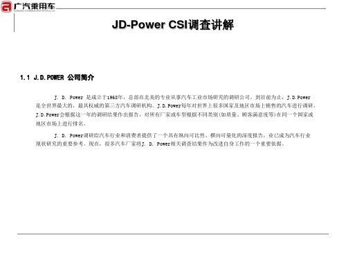
J.D. Power目录编辑本段J.D. Power简介J.D.Power建立于1968年,是一家全球性的市场咨询公司,主要就顾客满意度,产品质量和消费者行为等方面进行独立公正的调研。
J.D.Power业务包括行业范围的联合调研;定制(授权)跟踪调研;媒体调研;预测服务;培训服务以及在用户满意度和质量方面的商业运行分析和咨询。
2005年4月1日,J.D. Power and Associates加盟McGraw-Hill 公司,成为McGraw-Hill旗下的一个独立品牌。
在美国,J.D. Power and Associates最初因为其在汽车行业的业务而广为人知。
然而近些年来,公司将其业务扩展到了许多其它的行业,诸如电信、旅游和宾馆、海运、公用事业、卫生保健、民用建筑、消费电子以及财经服务。
洲太平洋地区服务的国J.D. Power亚太公司帮助客户理解在整个地区内影响质量和顾客满意度感知的因素。
公司的调研使客户可以知己知彼地做出战略决定,并且公司也量身定做产品,适应世界各国不同市场的消费者需求。
编辑本段J.D. Power在中国J.D. Power亚太公司于2005年春在上海设立了中国第一家分支机构,于2006年在华成功收购了Automotive Resources Asia (亚汽资源公司)。
在中国,公司现开展的业务包括行业内的联合调研、客户授权的定制调研、跟踪调研、汽车预测、企业培训、工作改进、运营分析和对产品质量以及用户满意度的咨询服务。
主要涉及的行业包括汽车、复印机、打印机。
公司有望在今年开展零售银行和网上调研业务。
J.D. Power and Associates 每年都会对全世界数以百万计的消费者进行调研,收集他们对很多行业产品与服务的感受和期望,并应制造商和供应商的要求向其提供预测,从而让当今信息更为灵通的消费者满意。
该公司进行的独立调查可向相关企业提供有价值的信息,帮助他们根据顾客的意见更好地了解他们的长处和不足。
UG0872User Guide PolarFire MPF300T FPGA Video KitJune 20191Revision History (1)1.1Revision 1.0 (1)2Introduction (2)2.1Kit Contents (2)2.2Block Diagram (2)2.3Board Overview (3)3Hardware Settings (6)3.1Jumper Settings (6)3.2LEDs (6)3.3Power Sources (7)4Board Components and Operations (9)4.1Memory Interface (9)4.2SPI Serial Flash (9)4.3HDMI1.4 Interface (10)4.4MIPI-RX Connector (CSI-2 Application) (10)4.5MIPI-TX Connector (DSI Application) (11)4.6MIPI-TX Connector (CSI-2 Application) (11)4.7MIPI-TX and RX PCB Loopback (12)4.8Transceivers (12)4.8.1XCVR0 Block (12)4.8.2XCVR1 and XCVR3 Blocks (13)4.8.3XCVR2 Block (14)4.8.4XCVR Reference Clock (15)4.9Programming (15)4.9.1FTDI and JTAG Header Scheme (15)4.1050 MHz Oscillator (16)4.11Device Reset (17)4.12User Reset (17)4.13User Interface (17)4.13.1User LEDs (18)4.13.2Push-Button Switches (18)4.13.3Slide Switches (DPDT) (19)4.13.4DIP Switches (SPST) (19)4.13.5FMC HPC Connector (J14) (20)4.14Board Components Placement (20)The revision history describes the changes that were implemented in the document. The changes arelisted by revision, starting with the most current publication.1.1Revision 1.0Revision 1.0 was the first publication of this documentThe Microsemi PolarFire® FPGA Video Kit (POLARFIRE VIDEO KIT), which is RoHS-compliant, enables youMPF300T-1FCG1152Eto evaluate the PolarFire FPGA for the following interfaces:MIPI CSI-2 RX interfaceHDMI2.0HDMI1.4DDR4 memoryFMC HPC with 8 Transceiver lanesUART Interface to the FTDI deviceSPI Interface to the SPI Flash device2.1Kit ContentsThe following table lists the contents of the PolarFire Video Kit.Table 1 • Kit ContentsItem QuantityDual Camera Sensor Module1PolarFire Video Board featuring the device with 300K logic elementsMPF300T-1FCG1152E 112 V, 5 A AC power adapter and cord1USB 2.0 A-male to mini-B cable programming1Quickstart card1Free one-year Libero Gold software license12.2Block DiagramThe following figure shows the block diagram of the video kit.Figure 1 • Block Diagram2.3Board OverviewThe following figure shows a labeled image of the video board highlighting its components.Figure 2 • Board CalloutThe following table lists the components of the video board.Table 2 • Board ComponentsComponent Label onBoardDescriptionFeatured DevicePolarFire FPGA FPGAMPF300T-1FCG1152EPower Supply12 V power supply J20The board is powered by a 12 V power source using an external +12 V/5 A DC jack ON/OFF switch SW4Power ON/OFF switch from +12 V external DC jackClocksOn-board 50 MHzclock oscillatorX350 MHz clock oscillator with single-ended outputXCVR reference clock Y5148.5 MHz oscillator (differential LVDS output) that provides reference clock(REFCLK) via PolarFire device pins AF29 and AF30. These pins are connected to theXCVRClock Synthesizer U15CDCEL913PWR Clock Synthesizer for HDMI1.4 clocks and programmable throughthe I2CFPGA Programming and DebuggingFT4232H U70USB-to-quad serial ports in various configurationsJTAG programming header J18This header is used to program and debug the PolarFire device using FlashPro4 or FlashPro5. In the FlashPro software, the appropriate programmer (FlashPro4orFlashPro5) must be selected.SPI flash U30One 1 Gb SPI Flash from Micron MT25QL01GBBB8ESF-0SIT (P/N) connected to SPIpins on bank 3 of the PolarFire deviceMemory ChipsDDR4 Memory U1,U2,U3 andU4Four 4 Gb (MT40A256M16GE-083E:B) chips are connected in Fly-by topology with a 64-bit data bus for storing data bitsFMC HPC connector J14FMC connector with eight XCVR lanes and 13 Differential pairs HPC[HA0:12] and LPC[0:33])Video InterfacesCSI-2 RX connector J5MIPI data and clock signals are received from Camera sensor boardDSI TX connector J26MIPI data and clock signals are transmitted to Display daughter board through theconnectorCS-2 TX connector J4MIPI data and clock signals are transmitted to Display daughter board through theconnectorGeneral Purpose I/OSwitches SW1 andSW2Push-button switches for user-interface debugging applicationsDIP Switches SW6Four DIP switches for testingLight-emitting diodes (LEDs)Four active-high LEDs connected to some of the user I/Os for debugging, and twelve active high LEDs used for indicating power supplyComponent Label onBoardUSER Reset switch SW3Push-button system reset for the PolarFire device Users must program this HSIO forPolarFire logic reset functionDevice reset SW5Device reset3Hardware SettingsThis section provides information about jumper settings, switches, LEDs, and DIP switches on thePolarFire video board.3.1Jumper SettingsConnect the jumpers according to the settings specified in the following table.Table 3 • Jumper SettingsJumper Description Pin(s)DefaultJ15SPI Slave and Master mode selection. By DefaultSPI master1-2Closed J19XCVR_VREF is connected to GND1-2ClosedJ28Close pin 1-2 to program through the FTDI Openpin 1-2 to program the external Flash pro51-2ClosedJ24Jumper to select the PolarFire VDDAUX4 for Bank4 voltage Close pin2-4 for 3V3Close pin2-4 for 2V5ClosedOpenJ25Jumper to select the PolarFire VCCIO voltage (VCCIO_HPC_VADJ)Close pin 1 and 2 for 3.3 VClose pin 3 and 4 for 2.5 VClose pin 5 and 6 for 1.8 VClose pin 7 and 8 for 1.5 VClose pin 9 and 10 for 1.2 VOpenOpenClosedOpenOpenJ36Jumper to select the SW3 input or theENABLE_FT4 232 signal from the FT4232H chip Close pin 1 and 2 for manual power switchingusing SW3Close pin 2 and 3 for remote power switchingusing the GPIO capability of the FT4232 chipCloseOpen3.2LEDsThe following table lists the power supply LEDs.Table 4 • LEDsLED DescriptionDS14-Green12 V voltage railDS20-Green 5 V voltage railDS21-Green 3.3V voltage railDS5-Green 1.0V voltage railDS4-Green 1.8V voltage railDS3-Green VDD25 Voltage railDS2-Green VDDAUX2_5 Voltage railLED DescriptionDS9-Green VDDA(1V05) Voltage railDS8-Green VDDAUX4 Voltage railDS7-Green 1.2V voltage railDS6-Green VCCIO_HPC_VADJ voltage railDS12-Green 1.8V HDMI1V4 voltage railDS13-Green0.6V VTT voltage rail3.3Power SourcesThe PolarFire video board uses Microchip power supply devices. For more information about thesepower supply devices, see: https:///design-centers/power-management/dc-dc-converters-regulators.The following table lists the key power supplies required for normal operation of the PolarFire videoboard.Table 5 • Voltage Rails in PolarFire Video BoardPolarFire Bank I/O Rail VoltageBank 01P2V 1.2VBank 11P8V 1.8VBank 21P2V_B2 1.2VBank 3VDD25 2.5VBank 4VCCIO_HPC_VADJ 1.8VBank 5VDD25 2.5VBank 61P8V_HDMI1V4 1.8VBank 71P2V 1.2VThe following figure shows the power supply scheme used in the PolarFire video board.Figure 3 • Power Supply SchemeThe following table lists the suggested Microchip power regulators for PolarFire FPGA voltage rails.Table 6 • Power RegulatorsVoltage Rail Part Number Description Current5V MIC24055YJL-TR IC REG BUCK ADJ 12A SYNC 28QFN12A1V MIC24055YJL-TR IC REG BUCK ADJ 12A SYNC 28QFN12A1V2MIC24046YFL-TR IC REG BUCK PROG 5A SYNC 20VQFN5AVDDAUX2&5MIC23303YML-T5IC REG BUCK ADJ 3A SYNC 12DFN3AVDDAUX4MIC23303YML-T5IC REG BUCK ADJ 3A SYNC 12DFN3AVCCIO_HPC_VADJ MIC24046YFL-TR IC REG BUCK PROG 5A SYNC 20VQFN5AVREF,VTT MIC5166YML-TR IC PWR SUP 3A HS DDR TERM 10MLF3AHDMI1.4MCP1726T-ADJE/MF IC REG LINEAR POS ADJ 1A 8DFN1AVDD25MIC69502WR IC REG LINEAR POS ADJ 5A SPAK-75A3V3MIC69502WR IC REG LINEAR POS ADJ 5A SPAK-75AVDD18MIC69502WR IC REG LINEAR POS ADJ 5A SPAK-75A1V05MIC69502WR IC REG LINEAR POS ADJ 5A SPAK-75ANote: These regulators are not pin compatible with the existing video kit schematics. Use these regulators for new board.4Board Components and OperationsThis section describes the key components of the PolarFire Video board and important boardoperations.4.1Memory InterfaceThe following figure shows the memory interface scheme.Figure 4 • Memory InterfaceAs shown in the preceding figure, Four 4 Gb DDR4 SDRAM chips are used as flexible volatile memory foruser applications. The DDR4 interface is implemented in the HSIO Bank 0 and Bank 7.The DDR4 SDRAM specifications are as follows:MT40A256M16GE-083E:BQuantity: Four chips are connected in Fly-by topologyDensity: 16 GbData rate: DDR4 64-bit at 166 MHz clock rateThe PolarFire video board design uses the DDR4 and POD12 standards for the DDR4 interface. Thedefault board assembly for the DDR4 standard uses RC terminations.4.2SPI Serial FlashThe following figure shows the SPI Flash and its interface with the PolarFire device.The SPI flash specifications for the PolarFire device are:Density: 1 GbVoltage: 2.7 V to 3.6 V (MT25QL01GBBB8ESF-0SIT)Frequency: 90 MHz Quantity = 1SPI mode support: Modes 0 and 34.3HDMI1.4 InterfaceOne HDMI1.4 Transmitter is connected to the PolarFire device to support the HDMI1.4 standard as shown in the following figure.Figure 6 • HDMI1.4 InterfaceThe HDMI interface is implemented in Bank6.The HDMI1.4 transmitter specifications for the PolarFire device are:Part Number of the HDMI Transmitter: ADV7511KSTZ Operating frequency: up to 225 MHz4.4MIPI-RX Connector (CSI-2 Application)The video board supports a dual Camera image sensor daughter card that can be connected using the CSI-2 RX interface (J5) for CSI-2 RX applications. The daughter card includes two IMX334 cameras. Each image sensor supports a four-lane MIPI interface. The daughter card is connected to the video board via the board to board connector as shown in the following figure The MIPI output signals . (see page )are connected to Bank 2.The image sensor supports maximum 1782 Mbps.4.5MIPI-TX Connector (DSI Application)The video board supports the MIPI transmitter X4 lanes and clock for DSI application, as shown in thefollowing figure. MIPI TX signals are interfaced to the LCD display. An adaptor board for the LCD displaycan be connected through the J26 connector on the video board. This adaptor board contains the LCDmating connector and the auxiliary circuit required for the display. For more information, see the videoboard schematics.Figure 8 • MIPI-TX Connection (DSI Application)4.6MIPI-TX Connector (CSI-2 Application)The video board supports the MIPI X4 lanes and clock for the CSI-2 transmitter application, as shown inthe following figure. For testing, the video board can be can be interfaced with Nvidia’s Jetson TX1\TX2development board using a mating connector cable.Figure 9 • MIPI-TX Connection (CSI-2 Application)`4.7MIPI-TX and RX PCB LoopbackThe video board supports the on-board PCB trace loopback of MIPI X4 lanes and clock, as shown in thefollowing figure.Figure 10 • MIPI-TX and RX Loopback4.8TransceiversMPF300T-1FCG1152EThe PolarFire FPGA device has 4 XCVR blocks and each block contains 4transceiver lanes. These lanes can be accessed through the HDMI2.0 and FMC connectors on the board.The following sections describe these blocks and the lanes used.4.8.1XCVR0 BlockLanes 0, 1, and 2 of the XCVR0 block are looped back, as shown in the following figure .Figure 11 • XCVR0 Interface4.8.2XCVR1 and XCVR3 BlocksXCVR1 and XCVR3 blocks have four lanes each. These lanes are connected to the FMC HPC connectorand the signals are routed on the PCB as follows:Lanes 0 to 7 are directly routed to the FMC HPCTX pad > trace > via (to bottom layer) > trace > FMC HPC connector padRX pad > trace > via (to Top layer) > trace > PolarFire device padThe XCVR1 and XCVR3 reference clock is routed directly from the HPC connector to the PolarFire device.The following figure shows the XCVR1 and XCVR3 and their interfaces.Figure 12 • XCVR1 and XCVR3 Interface4.8.3XCVR2 BlockThe lanes of the XCVR2 block are connected to HDMI2.0 TX and RX chips via the line drivers chips, asshown in the following figure. This interface can operate up to 6 Gbps.Figure 13 • XCVR2 Interface4.8.4XCVR Reference ClockThe following figure shows the clock sources for XCVR blocks.Figure 14 • XCVR Reference ClocksXCVR 1A, 3A reference clocks are sources from FMC HPC connector(J14).XCVR 2B reference clock is sourced from the on-board 148.5 MHzXCVR 2A reference clock is sourced from the on-board HMDI2.0 TX4.9ProgrammingThe PolarFire device is programmed using the on-board FlashPro5 programmer or through the JTAGvideo board schematicsHeader. For more information about programming, see the .The following section describes the FTDI and JTAG Header programming schemes used on the board.4.9.1FTDI and JTAG Header SchemeThe PolarFire device can be programmed using the on-board JTAG Header or FTDI. By default, the FTDIprogramming mode is enabled. The programming mode can be changed based on the Jumper settings.Table 3For more information, see .The following figure shows how the JTAG Header interfaces with the PolarFire Device.Figure 15 • JTAG Header InterfaceNote: By default, the FTDI programming mode is enabled. Remove J28 jumper to enable programmingthrough JTAG header.4.1050 MHz OscillatorA 50 MHz clock oscillator with an accuracy of +/-50 ppm is available on the board. This clock oscillator isconnected to the FPGA fabric to provide a system reference clock. An on-chip PolarFire PLL can beconfigured to generate a wide range of high-precision clock frequencies.The package and pin details of the 50 MHz oscillator are as follows:Pin Number: AL26Pin Name: HSIO72PB1/CCC_NE_CLKIN_N_11 shows the 50 MHz clock oscillator interface.Figure 16 • 50 MHz Oscillator Interface4.11Device ResetAs shown in the following figure, DEVRST_N (SW5 push button) is an input-only reset switch that allowsassertion of a full reset of the chip at any time. The DEVRST_N signal is an active-low signal.Figure 17 • Device Reset4.12User ResetAs shown in the following figure the user reset (SW3 push button) is an input-only reset, (see page )switch that allows assertion of a reset of the fabric logic.Figure 18 • User Reset4.13User InterfaceLEDs and push-button switches are available on the board for the user interface.4.13.1User LEDs(see page ) Four active-high LEDs are connected to the PolarFire device. The following table lists theon-board label of these switches, the associated PolarFire pin number, name, and Bank.Table 7 • User LEDsLabel On Board PolarFire Pin Number PolarFire Pin Name PolarFire BankLED1G17HSIO37NB6Bank 6LED2K23HSIO54PB6Bank 6LED3L23HSIO54NB6Bank 6LED4B25HSIO68NB6/DQS Bank 6(see page )The following figure shows how each user LED interfaces with the PolarFire device.Figure 19 • User LED Interface4.13.2Push-Button SwitchesTwo push-button tactile switches are connected to the PolarFire device. The following table lists the on-board label of these switches, the associated PolarFire pin number, name, and Bank.Table 8 • Push-Button SwitchesLabel On Board PolarFire Pin Number PolarFire Pin Name PolarFire BankSW1AK20HSIO98NB1Bank 1SW2AM27HSIO73NB1Bank 1The following figure shows how these push-button switches interface with the PolarFire Device.4.13.3Slide Switches (DPDT)The SW4 slide switch powers the device ON or OFF.4.13.4DIP Switches (SPST)The SW6 DIP switch includes 8 connections to the PolarFire device. The following table lists on-boardlabel of these switches, the associated PolarFire pin number, name, and Bank.Table 9 • DIP SwitchLabel On Board PolarFire Pin Number PolarFire Pin Name PolarFire BankDIP1AH22HSIO99PB1/DQS Bank1DIP2AJ21HSIO99NB1/DQS Bank1DIP3AG21HSIO100PB1Bank1DIP4AH21HSIO100NB1Bank1The following figure shows how the DIP switch interfaces with the PolarFire device.4.13.5FMC HPC Connector (J14)An HPC (J14) FMC connector is available for future expansion of interfaces. This FMC connector iscompliant with the VITA 57.1 specification. The PolarFire Bank4, XCVR1, and XCVR3 signals are routed tothe FMC connector (J14) for user application development. For more information, see the video boardschematics.4.14Board Components PlacementThe following figure shows the top view of the placement of board components.Figure 22 • Silkscreen Top ViewThe following figure shows the bottom view of the placement of board components.Figure 23 • Silkscreen Bottom ViewMicrosemi HeadquartersOne Enterprise, Aliso Viejo,CA 92656 USAWithin the USA: +1 (800) 713-4113Outside the USA: +1 (949) 380-6100Sales: +1 (949) 380-6136Fax: +1 (949) 215-4996Email:***************************© 2019 Microsemi. All rights reserved. Microsemi and the Microsemi logo are trademarks of Microsemi Corporation. All other trademarks and service marks are the property of their respective owners.Microsemi makes no warranty, representation, or guarantee regarding the information contained herein or the suitability of its products and services for any particular purpose, nor does Microsemi assume any liability whatsoever arising out of the application or use of any product or circuit. The products sold hereunder and any other products sold by Microsemi have been subject to limited testing and should not be used in conjunction with mission-critical equipment or applications. Any performance specifications are believed to be reliable but are not verified, and Buyer must conduct and complete all performance and other testing of the products, alone and together with, or installed in, any end-products. Buyer shall not rely on any data and performance specifications or parameters provided by Microsemi. It is the Buyer's responsibility to independently determine suitability of any products and to test and verify the same. The information provided by Microsemi hereunder is provided "as is, where is" and with all faults, and the entire risk associated with such information is entirely with the Buyer. Microsemi does not grant, explicitly or implicitly, to any party any patent rights, licenses, or any other IP rights, whether with regard to such information itself or anything described by such information. Information provided in this document is proprietary to Microsemi, and Microsemi reserves the right to make any changes to the information in this document or to any products and services at any time without notice.Microsemi, a wholly owned subsidiary of Microchip Technology Inc. (Nasdaq: MCHP), offers a comprehensive portfolio of semiconductor and system solutions for aerospace & defense, communications, data center and industrial markets. Products include high-performance and radiation-hardened analog mixed-signal integrated circuits, FPGAs, SoCs and ASICs; power management products; timing and synchronization devices and precise time solutions, setting the world's standard for time; voice processing devices; RF solutions; discrete components; enterprise storage and communication solutions; security technologies and scalable anti-tamper products; Ethernet solutions; Power-over-Ethernet ICs and midspans; as well as custom design capabilities and services. Microsemi is headquartered in Aliso Viejo, California, and has approximately 4,800 employees globally. Learn more at www. .50200872。