LH1530中文资料
- 格式:pdf
- 大小:178.07 KB
- 文档页数:20
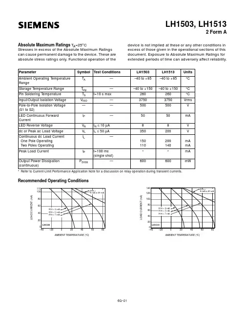
FEATURES•3750 Vrms or 5300 Vrms I/O isolation •Current-limit protection built-in•Linear ac/dc operation•High-reliability monolithic receptor •Extremely low leakage current (pA)•High contact off-impedance (G W)•Low power consumption (1 mW—12 mW)•Very low switch offset (typically 0.1 m V)•Logic compatible•Clean, bounce-free switching•Built-in 1 Form C break-before-make •High surge capability•Insensitive to dv/dt•Surface mountable•Compatible with UL1459 and FCC 68.302•UL recognized•CSA certified•BABT certificate of recognition to BS6301 BENEFITS•Long life•Maintenance free•Current-limit SSRs can sustainrepeated faults without damage •Minimizes drive circuitry•Noiseless•Immune to shock•Immune to environmental hazards such as salt, dirt, and humidity•No arcing•No mounting restrictions •Preapproved for DAA applications •High reliability•Easily configured in series or in parallel for increased voltage or current DESCRIPTIONSiemens Solid State Relays (SSRs) are miniature, optically-coupled relays with high-voltage MOSFET outputs. The relays are capable of switching ac or dc loads from as little as nanovolts to hundreds of volts. Likewise, the relays can switch currents in the range of nanoamps to hundreds of milli-amps. The MOSFET switches are ideal for small signal switching and are primarily suited for dc or audio frequency applications.Siemens offers integrated current limiting on many of its relays. If load current through the relay exceeds the rated value, the relay clamps the current at a predefined value. If the excessive load current persists, the limiting circuit has a foldback feature to minimize relay power dissipation. The current-limit circuit has a multitude of uses. It can be used in tele-phony to clamp excessive currents emanating from lightning strikes and/ or power-main crosses or in instrumentation and industrial application to squelch transients from reactive loads. The current-limit circuit also provides short-circuit protection in power-feed applications.The SSRs feature a monolithic output die that minimizes wire bonds and permits easy integration of high-performance circuits such as current limiting in normally-open switches. The output die contains all the neces-sary circuitry to perform a relay function, including the photodiode receptor array, turn-on and turn-off control circuitry, and the MOSFET switches. The optically-coupled input is controlled by a highly efficient GaAlAs infrared LED.Siemens SSRs are available in a 6- or 8-pin through-hole DIP or in gull-wing surface-mount packages. Some parts are also offered in 8- or 18-pin small-outline packages (SOPs). The SOPs are size and height compatible with PCMCIA Type 2 cards. A 0.4 mm distance through insulation spacing is also available on “H” suffix coded parts. Refer to the Parts Coding section for a more in-depth description of these parts.High Voltage Solid State RelaysGeneral InformationSiemens Microelectronics, Inc. • Optoelectronics Division 元器件交易网Typical Applications•ac Switch•Modems •Telephone•Programmable Controllers •Heater Control•FAX•Light Control•Data Acquisition Systems •Switching Systems•Security Equipment •Voltmeters•Electric Meters•Test Equipment•Ring RelayTypical Applications (continued)•Service Equipment•Thermostats•E&M Signaling•Answering Machines •Multiplexers•Battery Switch •Scanners•Board Testers •Motor Controls•Gas Pumps •Output Modules•Appliances元器件交易网元器件交易网 Wiring DiagramsAbsolute Maximum Ratings T A =25 ° CStresses in excess of the Absolute Maximum Ratings can cause permanent damage to the device. These are absolute stress ratings only. Functional operation of the device is not implied at these or any other conditions in excess of those given in the operational sections of this document. Exposure to Absolute Maximum Ratings for extended periods of time can adversely affect reliability. *5300 Vrms input/output isolation voltage available on some products. Consult factory.†Refer to Current Limit Performance Application Note 58 for a discussion on relay operation during transient currents.Parameter Symbol Test Conditions LH1500LH1504LH1510LH1516Units Ambient Operating Temperature rangeT A —–40 to +85 ° CStorage Temperature Range T stg —–40 to +150Pin Soldering Temperature T S t=10 s max 260Input/Output Isolation Voltage*V ISO —3750Vrms LED Continuous Forward CurrentI F —50mA LED Reverse Voltage V R I R £ 10 m A 8Vdc or Peak ac Load VoltageV L I L £ 50 m A 350400200400Continuous dc Load Current Bidirectional Operation Unidirectional Operation I L—15025095—200350240450mA Peak Load Current I P t=100 ms (single shot)††††mA Output Power Dissipation (continuous)P DISS—600550600mWLH1500, LH1504LH1510, LH15161 Form ARecommended Operating ConditionsAMBIENT TEMPERATURE (°C)L O A D C U R R E N T (m A )AMBIENT TEMPERATURE (°C)L O A D C U R R E N T (m A )AMBIENT TEMPERATURE (°C)L O A D C U R R E N T (m A )L O A D C U R R E N T (m A )AMBIENT TEMPERATURE (°C)元器件交易网Electrical Characteristics T A =25 ° CMinimum and maximum values are testing requirements. Typical values are characteristics of the device and are the result of engineering evaluations. Typical values are for information purposes only and are not part of the testing requirements. .*R ON =V (50 mA) – V (20 mA)/30 mA, †I F =10 mA.ParameterSymbol Test Conditions Values LH1500LH1504LH1510LH1516Units I N P U TLED Forward Currentfor Switch Turn-on I FonI L =100 mA t=10 ms Min————mA Typ 1.00.5 1.00.9mA Max 2.0 2.0 2.0 2.0mA LED Forward Current for Switch Turn-offI FoffMin 0.20.10.20.2mA Typ 0.90.40.90.8mA Max ————mA V L± 300350150350V LED Forward VoltageV FI F =10 mA Min 1.15 1.15 1.15 1.15V Typ 1.26 1.26 1.26 1.26V Max 1.45 1.45 1.45 1.45V O U T P U TON-resistance ac/dcPin 4 ( ± ) to 6 ( ± ) dcPin 4, 6 (+) to 5 ( ± )R ONI F =5 mA I L =50 mAMin 1212*65 W Typ 2023*107 W Max 2534*1510 W I F =5 mA I L =100 mAMin 3.00— 1.50 1.25 W Typ 5.00— 2.50 2.00 W Max 6.25— 3.75 2.50 W OFF-resistanceR OFFI F =0 mA V L = ± 100 V Min 0.50.50.50.5G W Typ 5000500050002500G W Max ————G W ON-state Voltage —IL =1 mAMin — 1.2——V Typ — 1.4——V Max — 1.8——V I L =90 mA t=10 msMin — 3.0——V Typ — 3.6——V Max — 5.0——V Current Limit ac/dcPin 4 (±) to 6 (±)dcPin 4, 6 (+) to 5 (±)I LMTI F =5 mA t=5 msMin 230150300290mA Typ 270210360400mA Max 370270450550mA V L±61155V I F =5 mA, V L =4 V t=5 msMin ——600—mA Typ ——720—mA Max ——920—mA Off-stateLeakage Current—I F =0 mA V L =±100 V Min —— —nA Typ 0.020.020.020.04nA Max 200200200200nA I F =0mAMin ————m A Typ ————m A Max 1.0 1.0 1.0 1.0m A V L±350400200400V Output Capacitance Pin 4 to 6—I F =0 mA V L =1 V Min ————pF Typ 55 2.560150pF Max ————pF I F =0 mA V L =50 VMin ————pF Typ 1021530pF Max ————pF Switch Offset —I F =5mAMin ————m V Typ 0.15—0.150.1m V Max ————m V T R A N S F E RInput/Output Capaci-tance C ISO V ISO =1 VMin ————pF Typ 0.80.80.80.8pF Max ————pF Turn-on Timet onI F =5 mA I L =50 mA Min ————ms Typ 1.2 1.6 1.0† 1.1†ms Max 2.0 5.0 2.0† 3.0†ms Turn-off Timet offI F =5 mA I L =50 mAMin ————ms Typ 0.5 2.00.7†0.8†ms Max2.05.02.0†3.0†ms元器件交易网Absolute Maximum Ratings T A =25°CStresses in excess of the Absolute Maximum Ratings can cause permanent damage to the device. These are absolute stress ratings only. Functional operation of the device is not implied at these or any other conditions in excess of those given in the operational sections of this document. Exposure to Absolute Maximum Ratings for extended periods of time can adversely affect reliability.LH1517, LH1518, LH15191 Form AAMBIENT TEMPERATURE (°C)L O A D C U R R E N T (m A )AMBIENT TEMPERATURE (°C)L O A D C U R R E N T (m A )AMBIENT TEMPERATURE (°C)L O A D C U R R E N T (m A )Electrical Characteristics T A =25°CMinimum and maximum values are testing requirements. Typical values are characteristics of the device and are theresult of engineering evaluations. Typical values are for infor-mation purposes only and are not part of the testing require-ments.*I F =1.5 mA †I F =10 mA ‡ I L =25 mAParameterSymbol Test Conditions ValuesLH1517LH1518LH1519UnitsI N P U TLED Forward Current for Switch Turn-onI Fon I L =100 mA t=10 msMin ———mA Typ 0.90.80.9mA Max 2.0 2.0 2.0mA LED Forward Current for Switch Turn-off I FoffMin 0.20.20.2mA Typ 0.80.70.8mA Max ———mA V L±100200200V LED Forward Voltage V F I F =10 mA Min 1.15 1.15 1.15V Typ 1.26 1.26 1.26V Max 1.45 1.45 1.45V O U T P U TON-resistance ac/dcPin 4 (±) to 6 (±) dcPin 4, 6 (+) to 5 (±)R ONI F =5 mA I L =50 mA Min 1103W Typ 2156W Max 32010W I F =5 mA I L =100 mAMin 0.25 2.500.75W Typ 0.50 3.75 1.50W Max 0.85 5.00 2.50W OFF-resistance R OFF I F =0 mA V L =±100 V Min 0.50.50.5G W Typ 250050002500G W Max ———G W ON-state Voltage—I L =1 mA Min ———V Typ ———V Max ———V I L =90 mA t=10 msMin ———V Typ ———V Max ———V Current Limit ac/dcPin 4 (±) to 6 (±) dcPin 4, 6 (+) to 5 (±)I LMTI F =5 mA t=5 msMin —170330mA Typ —200450mA Max —280550mA VL±—64V I F =5 mA, V L =4 V t=5 msMin ———mA Typ ———mA Max ———mA Off-stateLeakage Current—I F =0 mA V L =±100 V Min ———nA Typ 0.040.020.04nA Max 200200200nA I F =0 mA Min ——— m A Typ ——— m A Max 1.0 1.0 1.0 m A V L±150250V Output Capacitance Pin 4 to 6—I F =0 mA V L =1 V Min ———pF Typ 18555100pF Max ———pF I F =0 mA V L =50 VMin ———pF Typ 451020pF Max ———pF Switch Offset —I F =5 mA Min ——— V Typ 0.10.150.1 V Max ——— V T R A N S F E RInput/Output Capaci-tance C ISO V ISO =1 V Min ———pF Typ 0.80.80.8pF Max ———pF Turn-on Time t on I F =5 mA I L =50 mA Min ———ms Typ 1.7† 1.4 2.0ms Max 3.0† 3.0 3.0ms Turn-off Timet offI F =5 mA I L =50 mAMin ———Typ 1.3†0.70.9ms Max3.0†3.03.0msAbsolute Maximum Ratings T A =25°CStresses in excess of the Absolute Maximum Ratings can cause permanent damage to the device. These are absolute stress ratings only. Functional operation of the device is not implied at these or any other conditions in excess of those given in the operational sections of this document. Exposure to Absolute Maximum Ratings for extended periods of time can adversely affect reliability.LH1530, LH1535, LH1540LH1541, LH15501 Form AAMBIENT TEMPERATURE (°C)L O A D C U R R E N T (m A )AMBIENT TEMPERATURE (°C)L O A D C U R R E N T (m A )50201030040L O A D C U R R E N T (m A )AMBIENT TEMPERATURE (°C)Electrical Characteristics T A =25°CMinimum and maximum values are testing requirements. Typical values are characteristics of the device and are theresult of engineering evaluations. Typical values are for infor-mation purposes only and are not part of the testing require-ments.*I F =5 mA.†I F =10 mA.‡ I L =100 mA, t=10 msParameterSymbol Test Conditions ValuesLH1530LH1535/LH1540LH1541LH1550UnitsI N P U TLED Forward Current for Switch Turn-onI Fon I L =100 mA t=10 msMin ———— mA Typ 1.0 1.00.6 1.2mA Max 2.0 2.0 2.0 2.5mA LED Forward Current for Switch Turn-off I FoffMin 0.20.20.10.01mA Typ 0.90.90.5 1.100mA Max ————mA V L±300350/300150300V LED Forward Voltage V F I F =10 mA Min 1.15 1.15 1.10* 1.10*V Typ 1.26 1.26 1.19* 1.19*V Max 1.45 1.45 1.45* 1.45*V O U T P U TON-resistance ac/dcPin 4 (±) to 6 (±) dcPin 4, 6 (+) to 5 (±)R ONI F =5 mA I L =50 mA Min 12127025‡W Typ 182011037‡W Max 252516050‡W I F =5 mA I L =100 mAMin 3.00 3.00——W Typ 5.00 5.00——W Max 6.25 6.25——W OFF-resistance R OFF I F =0 mA V L =±100 V Min 0.50.50.50.5G W Typ 50005000100005000G W Max ————G W ON-state Voltage—I L =1 mA Min ————V T yp ————V Max ————V I L =90 mA t=10 msMin ————V T yp ————V Max ————V Current Limit ac/dcPin 4 (±) to 6 (±) dcPin 4, 6 (+) to 5 (±)I LMTI F =5 mA t=5 msMin —170—150mA Typ —210—200mA Max —250—270mA V L±—6—13V I F =5 mA, V L =4 V t=5 msMin ————mA T yp ————mA Max ————mA Off-stateLeakage Current—I F =0 mA V L =±100 V Min ————nA Typ 0.10.320.40.3nA Max 200200200200nA I F =0 mA Min ———— m A T yp ———— m A Max 1.0 1.0 1.0 1.0 m A V L±350400/350200350V Output Capacitance Pin 4 to 6—I F =0 mA V L =1 V Min ————pF Typ 5555 4.840pF Max ————pF I F =0 mA V L = 50 VMin ————pF Typ 1010 3.68pF Max ————pF Switch Offset —I F =5 mA Min ———— V Typ 0.150.150.150.15 V Max ———— V T R A N S F E RInput/Output Capaci-tance C ISO V ISO =1 V Min ————pF Typ 0.80.80.80.8pF Max ————pF Turn-on Time t on I F =5 mA I L =50 mA Min ————ms Typ 0.5† 1.20.12 1.4ms Max 1.0† 2.00.25 3.0ms Turn-off Timet offI F =5 mA I L =50 mAMin ————ms Typ 0.5†0.50.030.5ms Max1†2.00.253.0msA. LED Voltage vs. TemperatureC. LED Current for Switch Turn-On vs. TemperatureE. Current Limit vs. TemperatureB. LED Dropout Voltage vs. TemperatureD. LED Current for Switch Turn-On vs. Temperature (LH1541)F. ON-Resistance vs. TemperatureAMBIENT TEMPERATURE (°C)L E D F O R W A R D V O L T A G E (V )1.61.51.41.01.31.21.1AMBIENT TEMPERATURE (°C)100–60LE DF O R W A R D C U R R E N T F O R S W I T C H T U R N -O N (%) N O R M A L I Z E D T O 25 °C806040–4020–200C H A N G E I N C U R R E N T L I M I T (%)N O R M A L I Z E D T O 25 °CAMBIENT TEMPERATURE (°C)160–6015012090–30–40–202040608060030AMBIENT TEMPERATURE (°C)L E D F O R W A R D C U R R E N T F O R S W I T C H T U R N -O N (%) N O R M A L I Z E D T O 25 °CC H A N G E I N O N -R E S I S T A N C E (%)N O R M A L I Z ED T O 25°CAMBIENT TEMPERATURE (°C)A. Variation in ON-Resistance vs. LED CurrentC. Switch Capacitance vs. Applied VoltageE. Switch Capacitance vs. Applied Voltage (LH1525)B. Variation in ON-Resistance vs. LED Current (LH1525)D. Switch Capacitance vs. Applied VoltageF. Switch Capacitance vs. Applied Voltage (LH1541)LED FORWARD CURRENT (mA)a c /d c O N -R E S I S T A N C E V A R I A TI O N (%) N O R M A L I Z E D T OD A T A S HE E T R O N S P E C IF I C A T I O N @ I F = 5 m AC A P A C I T A N C E (p F )80605004030201070APPLIED VOLTAGE (V)APPLIED VOLTAGE (V)02040706050604080100302010C A P A C I T A N C E (p F )LED FORWARD CURRENT (mA)0.01.02.07650 3.04 4.05.032189a c /d c O N -R E S IS T A N C E V A R I A T I O N (%)N O R M A L I Z E D T O D A T A S H E E T R O N S P E C I F I C A T I O N @ I F = 5 m AAPPLIED VOLTAGE (V)C A P A C I T A N C E (p F )804001020APPLIED VOLTAGE (V)C A P A C I T A N C E (p F )6.05.00.0304.0100403.02.01.05060708090A. Insertion Loss vs. FrequencyC. Insertion Loss vs. Frequency (LH1541)E. Leakage Current vs. Applied VoltageB. Insertion Loss vs. Frequency (LH1525)D. Output IsolationF. Leakage Current vs. Applied Voltage at Elevated TemperaturesFREQUENCY (Hz)I N S E R T I O N L O S S (d B )FREQUENCY (Hz)I N S E R T I O N L O S S (d B )10210310410590LOAD VOLTAGE (V)O F F -S T A T E L E A K A G E C U R R E N T (p A )7080604030502010FREQUENCY (Hz)I N S E R T I O N L O S S (d B )0.60.50.40.00.30.20.1FREQUENCY (Hz)I S O L A T I O N (d B )LOAD VOLTAGE (V)3.0O F F -S T A T E L E A KA G E C U R R E N T (n A )2.52.01.00.51.50A. Leakage Current vs. Applied Voltage at Elevated Temperatures (LH1525)C. Switch Breakdown Voltage vs. TemperatureE. Switch Offset Voltage vs. TemperatureB. Leakage Current vs. Applied Voltage at Elevated Temperatures (LH1541)D. Switch Breakdown Voltage vs. Temperature (LH1541)F. Switch Offset Voltage vs. Temperature (LH1525)LOAD VOLTAGE (V)3.00.0O F F -S T A T E L E A K A G E C U R R E N T (n A )2.52.01.00.50501001502002503003504001.53.5AMBIENT TEMPERATURE (°C)C H A N G E I N B R E A KD O W N V O L T A GE (%)N O R M A L I Z E D T O 25 °C80426–2–6–8–4AMBIENT TEMPERATURE (°C)S W I T C H O F F S E T V O L T A G E (µV )LOAD VOLTAGE (V)O F F -S T A T E L E A K A G E C U R R E N T (p A )AMBIENT TEMPERATURE (°C)–40–202040608084–8–10–6–4–2026C H A N G E I N B R E A K D O W N V O L T A G E (%)N O R M A L I Z E D T O 25 °CAMBIENT TEMPERATURE (°C)S W I T C H O F F S E T V O L T A G E (µV )A. Switch Offset Voltage vs. LED CurrentC. Switch Offset Voltage vs. LED Current (LH1541)E. Turn-On Time vs. Temperature (LH1541)B. Switch Offset Voltage vs. LED Current (LH1525)D. Turn-On Time vs. TemperatureF. Turn-Off Time vs. TemperatureLED FORWARD CURRENT (mA)S W I T C H O F F S E T V O L T A G E (µV )010LED FORWARD CURRENT (mA)S W I T C H O F F S E T V O L T A G E (µV )0.6152050.50.20.30.40.125AMBIENT TEMPERATURE (°C)C H A N G E I N T U R N -O N T I M E (%)N O R M A L I Z ED T O 25 °CLED FORWARD CURRENT (mA)05100.60.50.40.0150.3200.2250.1S W I T C H O F F S E T V O L T A G E (µV )AMBIENT TEMPERATURE (°C)C H A N G E I N T U R N -O N T I M E (%)N O R M A L I Z E D T O 25 °C6050–20–30–10010203040–40C H A N G E I N T U R N -O F F T I M E (%)N O R M A L I Z ED T O 25 °CAMBIENT TEMPERATURE (°C)A. Turn-Off Time vs. Temperature (LH1525)C. Turn-On Time vs. LED Current (LH1500, LH1518, LH1540)E. Turn-On Time vs. LED Current (LH1510)B. Turn-Off Time vs. Temperature (LH1541)D. Turn-On Time vs. LED Current (LH1504)F. Turn-On Time vs. LED Current (LH1516, LH1519)AMBIENT TEMPERATURE (°C)15105–150–5–10C H A N G E I N T U R N -O F F T I M E (%)N O R M A L I Z ED T O 25 °C1020LED FORWARD CURRENT (mA)T U R N -O N T I M E (m s )1086023045040LED FORWARD CURRENT (mA)T U R N -O N T I M E (m s )1086024–40–20020406080AMBIENT TEMPERATURE (°C)C H A N G E I N T U R N -O F F T I M E (%)N O R M A L I Z ED T O 25 °CT U R N -O N T I M E (m s )824610LED FORWARD CURRENT (mA)LED FORWARD CURRENT (mA)T U R N -O N T I M E (m s )108624A. Turn-On Time vs. LED Current (LH1517)C. Turn-On Time vs. LED Current (LH1530)E. Turn-Off Time vs. LED Current (LH1500, LH1530, LH1540)B. Turn-On Time vs. LED Current (LH1525)D. Turn-On Time vs. LED Current (LH1541)F. Turn-Off Time vs. LED Current (LH1504)T U R N -O N T I M E (m s )LED FORWARD CURRENT (mA)1086024LED FORWARD CURRENT (mA)T U R N -O N T I M E (m s )1086024T U R N -O F F T I M E (m s )LED FORWARD CURRENT (mA)LED FORWARD CURRENT (mA)3.02.41.80.01.2T U R N -O N T I ME (m s )LED FORWARD CURRENT (mA)T U R N -O N T I M E (m s )LED FORWARD CURRENT (mA)T U R N -O F F T I M E (m s )A. Turn-Off Time vs. LED Current (LH1510, LH1518)C. Turn-Off Time vs. LED Current (LH1517)E. Turn-Off Time vs. LED Current (LH1541)LED FORWARD CURRENT (mA)T U R N -O F F T I M E (m s )LED FORWARD CURRENT (mA)T U R N -O F F T I M E (m s )LED FORWARD CURRENT (mA)40302010T U R N -O F F T I M E (µs )B. Turn-Off Time vs. LED Current (LH1516, LH1519)D. Turn-Off Time vs. LED Current (LH1525)LED FORWARD CURRENT (mA)T U R N -O F F T I M E (m s )LED FORWARD CURRENT (mA)T U R N -O F F T I M E (m s )Typical Performance Characteristics, LH1550 A. LED Voltage vs. TemperatureE. Turn-Off Time vs. TemperatureB. LED Current for Switch Turn-On/Off vs. Temperature D. ON-Resistance vs. TemperatureF. Turn-Off Time vs. Temperature。