VISHAY威世TVS及ESD二极管选型手册
- 格式:pdf
- 大小:3.55 MB
- 文档页数:15
Tr a n s Z o r b®雪崩T V S PA R®汽车T V S特殊功能瞬态电压抑制器E S D保护器件Vishay 的TransZorb®瞬态电压抑制器(TVS )采用了目前最先进的技术,可提供业界最大的电压范围。
此设计允许雪崩击穿二极管TVS 在较短时间内吸收大量能量而不被损坏。
Vishay 的TransZorb TVS 没有耗损机制,具有足够快的导通时间和极佳的箝位特性。
TransZorb ® 雪崩 TVS注解:(1) 利用10/1000 μs 脉冲进行测量(2) 部件编号中,"xx" 代表V WM , "nn" 代表标称电压(3) 部件编号中"nn"表示标称电压,"xx"或(m )脚注表示最低电压。
目前正在计划实现更高的电压指标(可达600 V )。
请与当地销售商联系确定产品信息(4) 双向极性用后缀"C"或"CA"来表示(BZW04使用后缀"B")(5) 大部分TVS 产品取得了UL 标准497B 下保护器类别(QVGQ2)的认证,且单向和双向器件都采用文件号E136766。
具体信息请参考各自的数据手册。
瞬态电压抑制器Vishay 的汽车瞬态电压抑制器(TVS )利用了PAR®专利技术,相比于其他雪崩TVS 二极管,其可在更大的温度范围内(可达185 oC )表现出极佳的稳定性和功率处理能力。
本产品组合包含了专门用于负载突降浪涌保护的器件,封装类型有轴向和表面贴装两种。
注解:(1) 利用10/1000 μs 脉冲进行测量(2) 部件编号中,"xx" 代表V WM , "nn" 代表标称电压(3) 部件编号中”nn ”表示标称电压,”xx ”表示最小电压 (5) 所有汽车TVS 都仅为单向极性(6) 所有汽车TVS 都利用PAR 专利工艺技术实现优越的高温性能(7) 大部分TVS 产品取得了UL 标准497B 下保护器类别(QVGQ2)的认证,且单向和双向器件都采用文件号E136766。
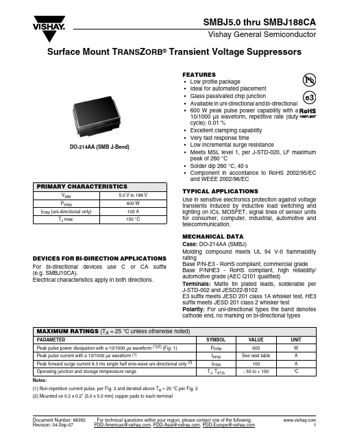
SMBJ5.0 thru SMBJ188CAVishay General SemiconductorDocument Number: 88392For technical questions within your region, please contact one of the following:Surface Mount T RANS Z ORB ® Transient Voltage SuppressorsFEATURES•Low profile package•Ideal for automated placement •Glass passivated chip junction••cycle): 0.01 %•Excellent clamping capability •Very fast response time•Low incremental surge resistance•Meets MSL level 1, per J-STD-020, LF maximum peak of 260 °C•Solder dip 260 °C, 40 s •Component in accordance to RoHS 2002/95/EC and WEEE 2002/96/EC TYPICAL APPLICATIONSUse in sensitive electronics protection against voltage transients induced by inductive load switching and lighting on ICs, MOSFET, signal lines of sensor units for consumer, computer, industrial, automotive and telecommunication.MECHANICAL DATA Case: DO-214AA (SMBJ)Molding compound meets UL 94 V-0 flammabilityratingBase P/N-E3 - RoHS compliant, commercial grade Base P/NHE3 - RoHS compliant, high reliability/automotive grade (AEC Q101 qualified)Terminals: Matte tin plated leads, solderable per J-STD-002 and JESD22-B102E3 suffix meets JESD 201 class 1A whisker test, HE3suffix meets JESD 201 class 2 whisker testPolarity: For uni-directional types the band denotes cathode end, no marking on bi-directional typesDEVICES FOR BI-DIRECTION APPLICATIONS For bi-directional devices use C or CA suffix (e.g. SMBJ10CA).Electrical characteristics apply in both directions.PRIMARY CHARACTERISTICSV WM 5.0 V to 188 VP PPM600 W I FSM (uni-directional only)100 A T J max.150 °CDO-214AA (SMB J-Bend)Notes:(1) Non-repetitive current pulse, per Fig. 3 and derated above T A = 25 °C per Fig. 2(2) Mounted on 0.2 x 0.2" (5.0 x 5.0 mm) copper pads to each terminalMAXIMUM RATINGS (T A = 25°C unless otherwise noted)PARAMETERSYMBOL VALUE UNIT Peak pulse power dissipation with a 10/1000 µs waveform (1)(2) (Fig. 1) P PPM 600 W Peak pulse current with a 10/1000 µs waveform (1)I PPM See next table A Peak forward surge current 8.3 ms single half sine-wave uni-directional only (2) I FSM 100 AOperating junction and storage temperature range T J , T STG- 55 to + 150°CSMBJ5.0 thru SMBJ188CAVishay General Semiconductor For technical questions within your region, please contact one of the following:Document Number: 88392ELECTRICAL CHARACTERISTICS (T A = 25°C unless otherwise noted)DEVICE TYPE MODIFIED“J” BEND LEADDEVICE MARKINGCODE BREAKDOWN VOLTAGE V BR AT I T (1)(V) TEST CURRENTI T (mA) STAND-OFF VOLTAGE V WM (V)MAXIMUM REVERSE LEAKAGE AT V WM I D (µA) (3)MAXIMUM PEAK PULSE SURGE CURRENT I PPM (A)(2)MAXIMUM CLAMPING VOLTAGE AT I PPMV C (V)UNIBIMIN.MAX.(+)SMBJ5.0 KD KD 6.40 7.82 10 5.0 800 62.5 9.6(+)SMBJ5.0A (5)KE KE 6.40 7.07 10 5.0 800 65.2 9.2(+)SMBJ6.0 KF KF 6.67 8.15 10 6.0 800 52.6 11.4 (+)SMBJ6.0A KG KG 6.67 7.37 10 6.0 800 58.3 10.3 (+)SMBJ6.5 KH AH 7.22 8.82 10 6.5 500 48.8 12.3 (+)SMBJ6.5A KK AK 7.22 7.98 10 6.5 500 53.6 11.2 (+)SMBJ7.0 KL KL 7.78 9.51 10 7.0 200 45.1 13.3 (+)SMBJ7.0A KM KM 7.78 8.60 10 7.0 200 50.0 12.0 (+)SMBJ7.5 KN AN 8.33 10.2 1.0 7.5 100 42.0 14.3 (+)SMBJ7.5A KP AP 8.33 9.21 1.0 7.5 100 46.5 12.9 (+)SMBJ8.0 KQ AQ 8.89 10.9 1.0 8.0 50 40.0 15.0 (+)SMBJ8.0A KR AR 8.89 9.83 1.0 8.0 50 44.1 13.6 (+)SMBJ8.5 KS AS 9.44 11.5 1.0 8.5 20 37.7 15.9 (+)SMBJ8.5A KT AT 9.44 10.4 1.0 8.5 20 41.7 14.4 (+)SMBJ9.0 KU AU 10.0 12.2 1.0 9.0 10 35.5 16.9 (+)SMBJ9.0A KV AV 10.0 11.1 1.0 9.0 10 39.0 15.4 (+)SMBJ10 KW AW 11.1 13.6 1.0 10 5.0 31.9 18.8 (+)SMBJ10A KX AX 11.1 12.3 1.0 10 5.0 35.3 17.0 (+)SMBJ11 KY KY 12.2 14.9 1.0 11 5.0 29.9 20.1 (+)SMBJ11A KZ KZ 12.2 13.5 1.0 11 5.0 33.0 18.2 (+)SMBJ12 LD BD 13.3 16.3 1.0 12 5.0 27.3 22.0 (+)SMBJ12A LE BE 13.3 14.7 1.0 12 5.0 30.2 19.9 (+)SMBJ13 LF LF 14.4 17.6 1.0 13 1.0 25.2 23.8 (+)SMBJ13A LG LG 14.4 15.9 1.0 13 1.0 27.9 21.5 (+)SMBJ14 LH BH 15.6 19.1 1.0 14 1.0 23.3 25.8 (+)SMBJ14A LK BK 15.6 17.2 1.0 14 1.0 25.9 23.2 (+)SMBJ15 LL BL 16.7 20.4 1.0 15 1.0 22.3 26.9 (+)SMBJ15A LM BM 16.7 18.5 1.0 15 1.0 24.6 24.4 (+)SMBJ16 LN LN 17.8 21.8 1.0 16 1.0 20.8 28.8 (+)SMBJ16A LP LM 17.8 19.7 1.0 16 1.0 23.1 26.0 (+)SMBJ17 LQ LQ 18.9 23.1 1.0 17 1.0 19.7 30.5 (+)SMBJ17A LR LR 18.9 20.9 1.0 17 1.0 21.7 27.6 (+)SMBJ18 LS BS 20.0 24.4 1.0 18 1.0 18.6 32.2 (+)SMBJ18A LT BT 20.0 22.1 1.0 18 1.0 20.5 29.2 (+)SMBJ20 LU LU 22.2 27.1 1.0 20 1.0 16.8 35.8 (+)SMBJ20A LV LV 22.2 24.5 1.0 20 1.0 18.5 32.4 (+)SMBJ22 LW BW 24.4 29.8 1.0 22 1.0 15.2 39.4 (+)SMBJ22A LX BX 24.4 26.9 1.0 22 1.0 16.9 35.5 (+)SMBJ24 L Y BY 26.7 32.6 1.0 24 1.0 14.0 43.0 (+)SMBJ24A LZ BZ 26.7 29.5 1.0 24 1.0 15.4 38.9 (+)SMBJ26 MD CD 28.9 35.3 1.0 26 1.0 12.9 46.6 (+)SMBJ26A ME CE 28.9 31.9 1.0 26 1.0 14.3 42.1 (+)SMBJ28 MF MF 31.1 38.0 1.0 28 1.0 12.0 50.0 (+)SMBJ28A MG MG 31.1 34.4 1.0 28 1.0 13.2 45.4 (+)SMBJ30 MH CH 33.3 40.7 1.0 30 1.0 11.2 53.5 (+)SMBJ30A MK CK 33.3 36.8 1.0 30 1.0 12.4 48.4 (+)SMBJ33 ML CL 36.7 44.9 1.0 33 1.0 10.2 59.0 (+)SMBJ33A MM CM 36.7 40.6 1.0 33 1.0 11.3 53.3 (+)SMBJ36 MN CN 40.0 48.9 1.0 36 1.0 9.3 64.3 (+)SMBJ36A MP CP 40.0 44.2 1.0 36 1.0 10.3 58.1 (+)SMBJ40 MQ CQ 44.4 54.3 1.0 40 1.0 8.4 71.4 (+)SMBJ40A MR CR 44.4 49.1 1.0 40 1.0 9.3 64.5SMBJ5.0 thru SMBJ188CAVishay General SemiconductorDocument Number: 88392For technical questions within your region, please contact one of the following:Notes:(1)Pulse test: tp ≤ 50 ms(2)Surge current waveform per Fig. 3 and derate per Fig. 2(3)For bi-directional types having V WM of 10 V and less, the I D limit is doubled (4)All terms and symbols are consistent with ANSI/IEEE C62.35(5)For the bi-directional SMBG/SMBJ5.0CA, the maximum V BR is 7.25 V (6)V F = 3.5 V at I F = 50 A (uni-directional only)(+)Underwriters laboratory recognition for the classification of protectors (QVGQ2) under the UL standard for safety 497B and file number E136766 for both uni-directional and bi-directional devices(+)SMBJ43 MS CS 47.8 58.4 1.0 43 1.0 7.8 76.7(+)SMBJ43A MT CT 47.8 52.8 1.043 1.0 8.6 69.4(+)SMBJ45 MU MU 50.0 61.1 1.0 45 1.0 7.5 80.3 (+)SMBJ45A MV MV 50.0 55.3 1.0 45 1.0 8.3 72.7 (+)SMBJ48 MW MW 53.3 65.1 1.0 48 1.0 7.0 85.5 (+)SMBJ48A MX MX 53.3 58.9 1.0 48 1.0 7.8 77.4 (+)SMBJ51 MY MY 56.7 69.3 1.0 51 1.0 6.6 91.1 (+)SMBJ51A MZ MZ 56.7 62.7 1.0 51 1.0 7.3 82.4 (+)SMBJ54 ND ND 60.0 73.3 1.0 54 1.0 6.2 96.3 (+)SMBJ54A NE NE 60.0 66.3 1.0 54 1.0 6.9 87.1 (+)SMBJ58 NF NF 64.4 78.7 1.0 58 1.0 5.8 103 (+)SMBJ58A NG NG 64.4 71.2 1.0 58 1.0 6.4 93.6 (+)SMBJ60 NH NH 66.7 81.5 1.0 60 1.0 5.6 107 (+)SMBJ60A NK NK 66.7 73.7 1.0 60 1.0 6.2 96.8 (+)SMBJ64 NL NL 71.1 86.9 1.0 64 1.0 5.3 114 (+)SMBJ64A NM NM 71.1 78.6 1.0 64 1.0 5.8 103 (+)SMBJ70 NN NN 77.8 95.1 1.0 70 1.0 4.8 125 (+)SMBJ70A NP NP 77.8 86.0 1.0 70 1.0 5.3 113 (+)SMBJ75 NQ NQ 83.3 102 1.0 75 1.0 4.5 134 (+)SMBJ75A NR NR 83.3 92.1 1.0 75 1.0 5.0 121 (+)SMBJ78 NS NS 86.7 106 1.0 78 1.0 4.3 139 (+)SMBJ78A NT NT 86.7 95.8 1.0 78 1.0 4.8 126 (+)SMBJ85 NU NU 94.4 115 1.0 85 1.0 4.0 151 (+)SMBJ85A NV NV 94.4 104 1.0 85 1.0 4.4 137 (+)SMBJ90 NW NW 100 122 1.0 90 1.0 3.8 160 (+)SMBJ90A NX NX 100 111 1.0 90 1.0 4.1 146 (+)SMBJ100 NY NY 111 136 1.0 100 1.0 3.4 179 (+)SMBJ100A NZ NZ 111 123 1.0 100 1.0 3.7 162 (+)SMBJ110 PD PD 122 149 1.0 110 1.0 3.1 196 (+)SMBJ110A PE PE 122 135 1.0 110 1.0 3.4 177 (+)SMBJ120 PF PF 133 163 1.0 120 1.0 2.8 214 (+)SMBJ120A PG PG 133 147 1.0 120 1.0 3.1 193 (+)SMBJ130 PH PH 144 176 1.0 130 1.0 2.6 231 (+)SMBJ130A PK PK 144 159 1.0 130 1.0 2.9 209 (+)SMBJ150 PL PL 167 204 1.0 150 1.0 2.2 268 (+)SMBJ150A PM PM 167 185 1.0 150 1.0 2.5 243 (+)SMBJ160 PN PN 178 218 1.0 160 1.0 2.1 287 (+)SMBJ160A PP PP 178 197 1.0 160 1.0 2.3 259 (+)SMBJ170 PQ PQ 189 231 1.0 170 1.0 2.0 304 (+)SMBJ170A PR PR 189 209 1.0 170 1.0 2.2 275 SMBJ188 PT PT 209 255 1.0 188 1.0 1.7 344 SMBJ188A PS PS 209 231 1.0 188 1.0 2.0 328ELECTRICAL CHARACTERISTICS (T A = 25°C unless otherwise noted)DEVICE TYPE MODIFIED“J” BEND LEADDEVICE MARKINGCODE BREAKDOWN VOLTAGE V BR AT I T (1)(V) TEST CURRENTI T (mA) STAND-OFF VOLTAGE V WM (V)MAXIMUM REVERSE LEAKAGE AT V WM I D (µA) (3)MAXIMUM PEAK PULSE SURGE CURRENT I PPM (A) (2)MAXIMUM CLAMPING VOLTAGE AT I PPMV C (V)UNIBIMIN.MAX.SMBJ5.0 thru SMBJ188CAVishay General Semiconductor For technical questions within your region, please contact one of the following:Document Number: 88392Note:(1) Mounted on minimum recommended pad layoutNote:(1) Automotive grade AEC Q101 qualifiedRATINGS AND CHARACTERISTICS CURVES (T A = 25 °C unless otherwise noted)THERMAL CHARACTERISTICS (T A = 25°C unless otherwise noted)PARAMETERSYMBOL VALUEUNITTypical thermal resistance, junction to ambient (1)R θJA 100 °C/WTypical thermal resistance, junction to lead R θJL20 °C/WORDERING INFORMATION (Example)PREFERRED P/N UNIT WEIGHT (g)PREFERRED PACKAGE CODEBASE QUANTITYDELIVERY MODESMBJ5.0A-E3/520.096527507" diameter plastic tape and reel SMBJ5.0A-E3/5B 0.0965B 320013" diameter plastic tape and reel SMBJ5.0AHE3/52 (1)0.096527507" diameter plastic tape and reel SMBJ5.0AHE3/5B (1)0.0965B320013" diameter plastic tape and reelFigure 1. Peak Pulse Power Rating Curve Figure 2. Pulse Power or Current vs. Initial Junction TemperatureFigure 3. Pulse WaveformFigure 4. Typical Junction CapacitanceSMBJ5.0 thru SMBJ188CAVishay General SemiconductorDocument Number: 88392For technical questions within your region, please contact one of the following:PACKAGE OUTLINE DIMENSIONS in inches (millimeters)Figure 5. Typical Transient Thermal ImpedanceFigure6. Maximum Non-Repetitive Peak Forward Surge CurrentDisclaimer Legal Disclaimer NoticeVishayALL PRODUCT, PRODUCT SPECIFICATIONS AND DATA ARE SUBJECT TO CHANGE WITHOUT NOTICE TO IMPROV E RELIABILITY, FUNCTION OR DESIGN OR OTHERWISE.Vishay Intertechnology, Inc., its affiliates, agents, and employees, and all persons acting on its or their behalf (collectively,“Vishay”), disclaim any and all liability for any errors, inaccuracies or incompleteness contained in any datasheet or in any other disclosure relating to any product.Vishay makes no warranty, representation or guarantee regarding the suitability of the products for any particular purpose or the continuing production of any product. To the maximum extent permitted by applicable law, Vishay disclaims (i) any and all liability arising out of the application or use of any product, (ii) any and all liability, including without limitation special, consequential or incidental damages, and (iii) any and all implied warranties, including warranties of fitness for particular purpose, non-infringement and merchantability.Statements regarding the suitability of products for certain types of applications are based on Vishay’s knowledge of typical requirements that are often placed on Vishay products in generic applications. Such statements are not binding statements about the suitability of products for a particular application. It is the customer’s responsibility to validate that a particular product with the properties described in the product specification is suitable for use in a particular application. Parameters provided in datasheets and/or specifications may vary in different applications and performance may vary over time. All operating parameters, including typical parameters, must be validated for each customer application by the customer’s technical experts. Product specifications do not expand or otherwise modify V ishay’s terms and conditions of purchase, including but not limited to the warranty expressed therein.Except as expressly indicated in writing, Vishay products are not designed for use in medical, life-saving, or life-sustaining applications or for any other application in which the failure of the Vishay product could result in personal injury or death. Customers using or selling Vishay products not expressly indicated for use in such applications do so at their own risk and agree to fully indemnify and hold Vishay and its distributors harmless from and against any and all claims, liabilities, expenses and damages arising or resulting in connection with such use or sale, including attorneys fees, even if such claim alleges that Vishay or its distributor was negligent regarding the design or manufacture of the part. Please contact authorized Vishay personnel to obtain written terms and conditions regarding products designed for such applications.No license, express or implied, by estoppel or otherwise, to any intellectual property rights is granted by this document or by any conduct of Vishay. Product names and markings noted herein may be trademarks of their respective owners.Document Number: 91000 。
TVS二极管选型指南一、选用指南1、首先确定被保护电路的最大直流或连续工作电压,电路的额定标准电压和“高端”容限。
2、TVS的额定反向关断电压V应大于或等于被保护电路的最大工作电压,WM太低,器件有可能进入雪崩状态或因反向漏电流太大影响电路的正若选用的VWM常工作。
应小于被保护电路的损坏电压。
3、TVS的最大箝位电压VC4、TVS的最大峰值脉冲功率PW必须大于被保护电路内可能出现的峰值脉冲功率。
5、在确定了TVS的最大箝位电压后,其峰值脉冲电流应大于瞬态浪涌电流。
6、对于数据接口电路的保护,必须注意选取尽可能小的电容值C的TVS器件。
7、带A的TVS二极管比不带A的TVS二极管的离散性要好,在TVS二极管A前面加C的型号表示双向TVS二极管。
8、直流保护一般选用单向TVS二极管,交流保护一般选用双向TVS二极管,多路保护选用TVS阵列器件,大功率保护选用TVS专用保护模块。
特殊情况,如:RS-485和RS-232保护可选用双向TVS二极管或TVS阵列。
9、TVS二极管可以在-55℃到+150℃之间工作,如果需要TVS在一个变化的温度下工作,由于其反向漏电流ID是随温度的增加而增大;功耗随TVS结温度增加而下降,故在选用TVS时应考虑温度变化对其特性的影响。
10、TVS二极管可以串/并应用,串行连接分电压,并行连接分电流。
但考虑到TVS的离散性,使用时应尽可能的减少串/并数量。
二、注解—是TVS最大连续工作的直流或脉冲电压,当这个反向电压加于TVS 1、VWM两极时,它处于反向关断状态,流过它的电流小于或等于其最大反向漏电流I。
D2、V—是TVS最小的雪崩电压。
25℃时,在这个电压之前,保护TVS是BR不导通的。
当TVS 流过规定的1mA电流I时,加于TVS两极间的电压为其最R小击穿电压VBR。
3、IT—--测试电流。
4、ID—--反向漏电流。
5、VC —当持续时间为20us的脉冲峰值电流IPP流过TVS时,其两极间出现的最大峰值电压为VC。


TVS、ESD管特性参数及选型TVS、ESD管特性参数及选型TVS二极管是专门设计用于吸收ESD能量并且保护系统免遭 ESD损害的固态元件。
如果应用得当,TVS二极管将限制跨在被保护器件上的电压刚好高过额定工作电压,但是却远低于破坏阈值电压。
T VS 相关参数处理瞬时脉冲对器件损害的最好办法是将瞬时电流从敏感器件引开。
TVS 二极管在线路板上与被保护线路并联,当瞬时电压超过电路正常工作电压后,TVS 二极管便发生雪崩,提供给瞬时电流一个超低电阻通路,其结果是瞬时电流通过二极管被引开,避开被保护器件,并且在电压恢复正常值之前使被保护回路一直保持截止电压。
当瞬时脉冲结束以后,TVS 二极管自动回复高阻状态,整个回路进入正常电压。
许多器件在承受多次冲击后,其参数及性能会发生退化,而只要工作在限定范围内,二极管将不会发生损坏或退化。
在选择TVS 二极管时,必须注意以下几个参数的选择:1. 最小击穿电压 VBR(M INIM UM BRE AKDOWN VOLT AGE)和击穿电流IR:VBR是TVS最小的击穿电压,在 25℃时,低于这个电压TVS是不会发生雪崩的。
当TVS流过规定的1mA 电流(IR)时,加于TVS 两极的电压为其最小击穿电压VBR。
按TVS的VBR与标准值的离散程度,可把 VBR分为5%和10%两种。
对于5%的VBR来说,VWM=0.85VBR;对于10%的VBR来说,VWM=0.81VBR。
为了满足IEC61000-4-2 国际标准,TVS二极管必须达到可以处理最小8kV(接触放电)和 15kV(空气放电)的ESD冲击,有的半导体生产厂商在自己的产品上使用了更高的抗冲击标准。
对于某些有特殊要求的便携设备应用,设计者可以按需要挑选器件。
2. 最大反向漏电流ID和额定反向关断电压VWM(RAT E D ST AND-OFF VOLT AGE):VWM这是二极管在正常状态时可承受的电压,此电压应大于或等于被保护电路的正常工作电压,否则二极管会不断截止回路电压;但它又需要尽量与被保护回路的正常工作电压接近,这样才不会在 TVS 工作以前使整个回路面对过压威胁。
TVS(瞬变抑制)二极管参数与选型TVS管的英文名是TRANSIENT VOLTAGE SUPPRESSOR,中文名叫瞬变抑制二极管。
它在承受瞬间高能量脉冲时,能在极短的内由原来的高阻抗状态变为低阻抗,并把电压箝制到特定的水平,从而有效的保护用户的设备和元器件不受损坏。
由于其具有箝位电压低、动作时间快等特点;因此比较适合于多级保护电路的末级保护。
此外也能和其它保护元件配合使用,组成专用的防雷装置。
目录TVS的参数特性TVS的应用TVS和其它浪涌保护元件的区别TVS的选用方法TVS管TVS的参数特性1.TVS特性TVS管是典型的PN结雪崩器件,和普通稳压管的击穿特性差不多。
但这条曲线只反映了TVS特性的一个部分,还必须补充下图所示的特性曲线,才能反映TVS的全部特性。
这是在双踪示波器上观察到的TVS管承受大电流冲击时的电流及电压波形。
图中曲线1是TVS管中的电流波形,它表示流过TVS管的电流由1mA突然上升到峰值,然后按指数规律下降,造成这种电流冲击的原因可能是雷击、过压等。
曲线2是TVS管两端电压的波形,它表示TVS中的电流突然上升时,TVS两端电压也随之上升,但最大只上升到VC值,这个值比击穿电压VBR略大,从而对后面的电路元件起到保护作用。
TVS在电路中和稳压管一样,是反向使用的。
2.参数说明A.击穿电压(VBR):TVS在此时阻抗骤然降低,处于雪崩击穿状态。
B.测试电流(IT):TVS的击穿电压VBR在此电流下测量而得。
一般情况下IT取1mA。
C.反向变位电压(VRWM):TVS的最大额定直流工作电压,当TVS两端电压继续上升,TVS将处于高阻状态。
此参数也可被认为是所保护电路的工作电压。
D.最大反向漏电流(IR):在工作电压下测得的流过TVS的最大电流。
E.最大峰值脉冲电流(IPP):TVS允许流过的最大浪涌电流,它反映了TVS的浪涌抑制能力。
F.最大箝位电压(VC):当TVS管承受瞬态高能量冲击时,管子中流过大电流,峰值为IPP,端电压由VRWM值上升到VC值就不再上升了,从而实现了保护作用。
TABLE OF CONTENTSIntroduction to Bare Die ......................................................................................................02Die Portfolio .........................................................................................................................03• Nomenclature ...............................................................................................................03• Infrared Emitters ...........................................................................................................04• Photodiodes .................................................................................................................06• Phototransistors ...........................................................................................................08Custom Design ....................................................................................................................09Packaging Options . (10)RESOURCES• Infrared emitter bare die product portfolio - /die-wafer/ir-emitting-diodes/• Photo detector bare die product portfolio - /die-wafer/photo-detectors/• For technical support contact -or • Sales contacts - /doc?99914Optoelectronics Bare Die Portfolio Infrared Emitters and Photo DetectorsIntroductionBenefits of using bare die• High design flexibility without package limitations• High level of integration• Temperature management with chip-on-board (COB) technology• Highly accurate die placement• Reduced system cost• Customer specific design• Possible process flow modificationVishay service• Design assistance• Assembly assistance• Die handling assistanceWafer processing duty• Wafer mapping/wafer inking• Wafer thinning• Wafer dicing• Die sorting• Visual inspectionPackaging and shipping methods• Unsawn wafer: the wafers are delivered in a sealed bag and die are not singulated• Sawn wafer on loose foil: the wafers are sawn and supplied on blue tape• Sawn wafer on discoframe: the wafers are sawn and supplied on a blue tape in a plastic frameDie Usage Basic GuidelinesBare die products require careful handling and storage as well as optimized assembly processes and tools to avoid damage and deviations from the expected performance. The following guidelines are based on Vishay’smany years of experience of manufacturing and assembling semiconductor devices.Die HandlingTo avoid contamination and damage die or wafers should never be handled by bare hands. Mechanical pressure has to be limited and special tweezers have to be used for grabbing a die from the packing.Storage time for wafers in sealed condition shall not exceed 6 months (storage ambient conditions: T A = 15...30 °C; relative humidity: < 60 %).Die AttachTo assure optimal electrical conductivity between silicon and copper, Vishay wafers are coated on the back side with two or three metallic solderable layers which are suitable for a wide range of solders, ranging from solder alloys to conductive epoxies. Fluxes are not recommended for solders because residuals can contaminate the surface of the die, and cause voids under the die, thus compromising heat dissipation and electrical performance.Vishay experts are happy to advise you on which assembly materials are best suited to your specific requirements..Wire BondingVishay does not define absolute bonding parameters, since bonding equipment and materials vary greatly. Customers are advised to optimize bonding parameters according to their specific equipment.Upon request, Vishay is ready to assist you in optimizing your wirebonding process.Infrared EmittersVishay offers a wide variety of high-power, high-speed infrared emitter chips for a broad range of applications. Vishay offers double heterojunction infrared emitters with the lowest forward voltages on the market; surface emitters that deliver the highest radiant intensities; and highly efficient homojunction emitters.All Vishay emitter chips satisfy the requirements of AEC Q101.PortfolioVishay offers a wide selection of chips, emitting at 830 nm, 850 nm, 870 nm, 890 nm, 940 nm and 950 nm.Typical Applications• IR touch display based devices such as printer displays, ebook reader, smart phones, tablets, and ultrabooks • Navigation devices• Automotive dashboard displays • Data communication • Illumination for camerasAvailable Technologies• Liquid Phase Epitaxy (LPE):– H omojunction structures on GaAs– D ouble heterojunction structures (DH) on GaAs/AlGaAs • Metal Organic Vapor Phase Epitaxy (MOVPE):– H igh-power surface emitter –B ulk emitterHomojunction Structure Surface EmitterDouble HeterojunctionStructureNote*The measurements are based on samples of die which are mounted on TO-18 gold header without resin coating.A I F =1A, B I F =250mA, C I F =100mA, D I F =70mA, E I F =50mAPhoto DetectorsVishay offers the broadest selection of high-speed, low dark current PIN photodiode chips. They are specially designed to achieve excellent sensitivity together with high reliability. Vishay phototransistors are extremely sensitive and fast compared to other such devices on the market.Portfolio• Vishay offers the broadest selection of photo detector chips suitable for ambient light and IR detection• Available technologies:–E pitaxial–H omogeneousTypical Applications• IR touch display based devices• High-speed data transfer• Light barriers• Position sensing• Alarm and safety equipmentCross Section of PIN Photodiode and PhototransistornPIN PhotodiodePhototransistorNote*The measurements are based on samples of die which are mounted on TO- header without resin coating **Binning is availableAmbient Light PIN PhotodiodesAmbient Light PhototransistorsNote*The measurements are based on samples of die which are mounted on TO- header without resin coatingCustom DesignVishay offers highly flexible design and fabrication of semi- and full custom specific photodiode and emitter chips. The huge variety of applications and assembly options requires bare die that are tailored to the specific application to keep the full potential of the device. A good fit between chip, assembly, and packaging is becoming ever more important with tighter space and power requirements.Vishay’s flexible technology base allows customization for a range of parameters and features as listed below:Emitters• Geometrical DesignChip outside dimensions, thickness, pad size, and shape and pad positions can be adjusted according to the customer specification.• P ad TopologyChip topology can be customized with respect to interconnect technology.Photodetectors• G eometrical DesignAlmost all geometrical parameters of a photodiode can be customized. This includes chip outside dimensions, chip thickness, pad size and shape, pad positions, photodiode position in an array, and alignment marks.• AR Coating / Optical FiltersDepending on impinging wavelength and application all photodiodes are equipped with an AR coating. Customization allows us to match the AR coating to the wavelength needed by the customer.• Pad TopologyDepending on interconnect technology pad topology can be also optimized.• PitchLinear or two-dimensional arrays with customizable pitch.Packing OptionsVishay provides you with several packing options which can fit with virtually any assembly line. Parts are 100 % probed and inspected.Unsawn waferDie are not singulated, wafers are provided in box.Sawn wafer on loose foilThe wafer is provided on blue film where dies are singulated, ready for pick and place, bad chips are removed, andmeasurement data is attached.The following documents are available upon the request:• Material content certificate–RoHS (DIN EN 62321)• H alogen free (DIN EN 14582)–SGA reports –Failure catalogue–ESD test results (according to the JEDEC standards)Sawn wafer on discoframeWafer is provided on blue foil; probed and inked; measurement data is attached.Upon request chips can also be delivered on plastic frames.For shipment, the wafers are arranged in stacks. The stacks are hermetically sealed in plastic bags to ensure protection against environmental influence (humidity and contamination).V I S H AY I N T E R T E C H N O L O GY, I NC.THIS DOCUMENT IS SUBJECT TO CHANGE WITHOUT NOTICE. THE PRODUCTS DESCRIBED HEREIN AND THIS DOCUMENT ARE SUBJECT TO SPECIFIC/doc?91000VMN-SG2200-150211/11SELECTOR GUIDE Bare DieOPTOELECTRONICSTHE AMERICASUNITED STATESVISHAY AMERICASONE GREENWICH PLACESHELTON, CT 06484UNITED STATESPH: +1-402-563-6866FAX: +1-402-563-6296ASIASINGAPOREVISHAY INTERTECHNOLOGY ASIA PTE LTD.37A TAMPINES STREET 92 #07-00SINGAPORE 528886PH: +65-6788-6668FAX: +65-6788-0988P .R. CHINAVISHAY CHINA CO., LTD.15D, SUN TONG INFOPORT PLAZA55 HUAI HAI WEST ROADSHANGHAI 200030P .R. CHINAPH: +86-21-22315555FAX: +86-21-22315551JAPANVISHAY JAPAN CO., LTD.SHIBUYA PRESTIGE BLDG. 4F3-12-22, SHIBUYASHIBUYA-KUTOKYO 150-0002JAPANPH: +81-3-5466-7150FAX: +81-3-5466-7160EUROPE GERMANY VISHAY ELECTRONIC GMBH DR.-FELIX-ZANDMAN-PLATZ 1 95100 SELB GERMANY PH: +49-9287-71-0 FAX: +49-9287-70435FRANCE VISHAY S.A.199, BD DE LA MADELEINE 06003 NICE, CEDEX 1 FRANCE PH: +33-4-9337-2727 FAX: +33-4-9337-2726UNITED KINGDOM VISHAY LTD.SUITE 6C, TOWER HOUSE ST. CATHERINE’S COURT SUNDERLAND ENTERPRISE PARK SUNDERLAND SR5 3XJ UNITED KINGDOM PH: +44-191-516-8584FAX: +44-191-549-9556WORLDWIDE SALES CONTACTS。