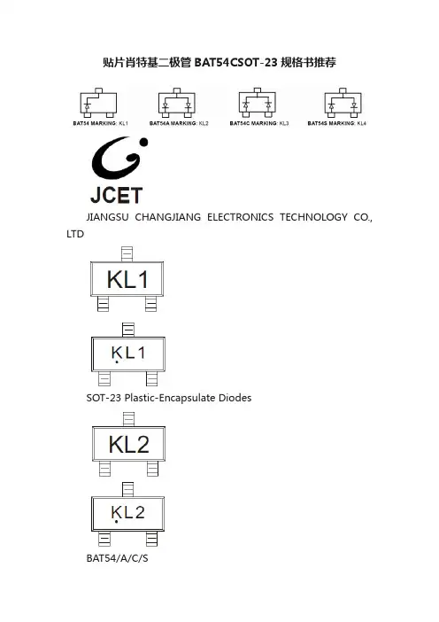
BAT54C 打标KL3肖特基二极管选型手册
- 格式:pdf
- 大小:949.58 KB
- 文档页数:3
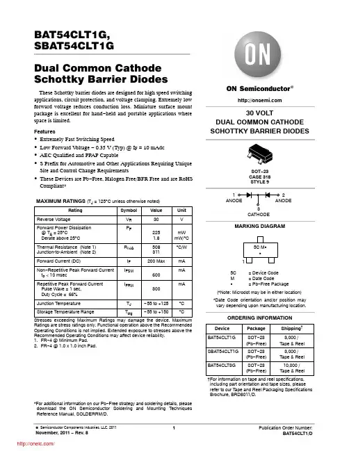
BAT54CLT1G,SBAT54CLT1GDual Common Cathode Schottky Barrier DiodesThese Schottky barrier diodes are designed for high speed switching applications, circuit protection, and voltage clamping. Extremely low forward voltage reduces conduction loss. Miniature surface mount package is excellent for hand−held and portable applications where space is limited.Features∙Extremely Fast Switching Speed∙Low Forward V oltage − 0.35 V (Typ) @ I F = 10 mAdc∙AEC Qualified and PPAP Capable∙S Prefix for Automotive and Other Applications Requiring Unique Site and Control Change Requirements∙These Devices are Pb−Free, Halogen Free/BFR Free and are RoHS Compliant*MAXIMUM RATINGS(T J = 125︒C unless otherwise noted)Rating Symbol Value Unit Reverse Voltage V R30VForward Power Dissipation @ T A = 25︒CDerate above 25︒C P F2251.8mWmW/︒CThermal Resistance (Note 1) Junction-to-Ambient (Note 2)R q JA508311︒C/WForward Current (DC)I F200 Max mANon−Repetitive Peak Forward Current t p < 10 msec I FSM600mARepetitive Peak Forward Current Pulse Wave = 1 sec,Duty Cycle = 66%IFRM300mAJunction Temperature T J−55 to +125︒C Storage Temperature Range T stg−55 to +150︒C Stresses exceeding Maximum Ratings may damage the device. Maximum Ratings are stress ratings only. Functional operation above the Recommended Operating Conditions is not implied. Extended exposure to stresses above the Recommended Operating Conditions may affect device reliability.1.FR−4 @ Minimum Pad.2.FR−4 @ 1.0 x 1.0 inch Pad.*For additional information on our Pb−Free strategy and soldering details, please download the ON Semiconductor Soldering and Mounting Techniques Reference Manual, SOLDERRM/D.30 VOLTDUAL COMMON CATHODE SCHOTTKY BARRIER DIODESCATHODE12MARKING DIAGRAM†For information on tape and reel specifications, including part orientation and tape sizes, please refer to our T ape and Reel Packaging Specifications Brochure, BRD8011/D.SOT−23CASE 318STYLE 95C= Device CodeM= Date CodeG= Pb−Free Package15C M GG*Date Code orientation and/or position mayvary depending upon manufacturing location.Device Package Shipping†ORDERING INFORMATIONBAT54CLT1G SOT−23(Pb−Free)3,000 /Tape & ReelBAT54CLT3G SOT−23(Pb−Free)10,000 /Tape & Reel (*Note: Microdot may be in either location) SBAT54CLT1G SOT−23(Pb−Free)3,000 /Tape & ReelELECTRICAL CHARACTERISTICS (T A = 25 C unless otherwise noted) (EACH DIODE)Characteristic Symbol Min Typ Max UnitReverse Breakdown Voltage (I R = 10 m A)V(BR)R30−−VTotal Capacitance(V R = 1.0 V, f = 1.0 MHz)C T−7.610pFReverse Leakage (V R = 25 V)I R−0.5 2.0m AForward Voltage (I F = 0.1 mAdc)V F−0.220.24VForward Voltage(I F = 30 mAdc)V F−0.410.5VForward Voltage(I F = 100 mAdc)V F−0.520.8VReverse Recovery Time(IF = I R = 10 mAdc, I R(REC) = 1.0 mAdc, Figure 1)trr−− 5.0nsForward Voltage(I F = 1.0 mAdc)V F−0.290.32VForward Voltage(I F = 10 mAdc)V F−0.350.40VNotes: 1. A 2.0 k W variable resistor adjusted for a Forward Current (I F) of 10 mA.2. Input pulse is adjusted so I R(peak) is equal to 10 mA.3. t p » t rrV Rt r10%90%IIOUTPUT PULSE(I F = I R = 10 mA; measuredat i R(REC) = 1 mA)INPUT SIGNALFigure 1. Recovery Time Equivalent Test CircuitC T , T O T A L C A P A C I T A N C E (p F )100V F , FORWARD VOLTAGE (VOLTS)101.00.110V R , REVERSE VOLTAGE (VOLTS)1.00.10.010.001140V R , REVERSE VOLTAGE (VOLTS)124205101530Figure 2. Forward VoltageFigure 3. Leakage CurrentFigure 4. Total Capacitance100100025206810I R , R E V E R S E C U R R E N T (m A )I F , F O R W A R D C U R R E N T (m A )PACKAGE DIMENSIONSSOT −23 (TO −236)CASE 318−08ISSUE APSTYLE 9:PIN 1.ANODE2.ANODE3.CATHODE*For additional information on our Pb −Free strategy and solderingdetails, please download the ON Semiconductor Soldering and Mounting Techniques Reference Manual, SOLDERRM/D.SOLDERING FOOTPRINT*NOTES:1.DIMENSIONING AND TOLERANCING PER ANSI Y14.5M, 1982.2.CONTROLLING DIMENSION: INCH.3.MAXIMUM LEAD THICKNESS INCLUDES LEAD FINISHTHICKNESS. MINIMUM LEAD THICKNESS IS THE MINIMUM THICKNESS OF BASE MATERIAL.4.DIMENSIONS D AND E DO NOT INCLUDE MOLD FLASH,PROTRUSIONS, OR GATE BURRS.VIEW CDIM A MIN NOM MAX MINMILLIMETERS0.89 1.00 1.110.035INCHES A10.010.060.100.001b 0.370.440.500.015c 0.090.130.180.003D 2.80 2.90 3.040.110E 1.20 1.30 1.400.047e 1.78 1.90 2.040.070L 0.100.200.300.0040.0400.0440.0020.0040.0180.0200.0050.0070.1140.1200.0510.0550.0750.0810.0080.012NOM MAX L1 2.10 2.40 2.640.0830.0940.104H E 0.350.540.690.0140.0210.0290−−−100−−−10q︒︒︒︒ON Semiconductor and are registered trademarks of Semiconductor Components Industries, LLC (SCILLC). SCILLC reserves the right to make changes without further notice to any products herein. SCILLC makes no warranty, representation or guarantee regarding the suitability of its products for any particular purpose, nor does SCILLC assume any liability arising out of the application or use of any product or circuit, and specifically disclaims any and all liability, including without limitation special, consequential or incidental damages.“Typical” parameters which may be provided in SCILLC data sheets and/or specifications can and do vary in different applications and actual performance may vary over time. All operating parameters, including “Typicals” must be validated for each customer application by customer’s technical experts. SCILLC does not convey any license under its patent rights nor the rights of others. SCILLC products are not designed, intended, or authorized for use as components in systems intended for surgical implant into the body, or other applications intended to support or sustain life, or for any other application in which the failure of the SCILLC product could create a situation where personal injury or death may occur. Should Buyer purchase or use SCILLC products for any such unintended or unauthorized application, Buyer shall indemnify and hold SCILLC and its officers, employees, subsidiaries, affiliates,and distributors harmless against all claims, costs, damages, and expenses, and reasonable attorney fees arising out of, directly or indirectly, any claim of personal injury or death associated with such unintended or unauthorized use, even if such claim alleges that SCILLC was negligent regarding the design or manufacture of the part. SCILLC is an Equal Opportunity/Affirmative Action Employer. This literature is subject to all applicable copyright laws and is not for resale in any manner.PUBLICATION ORDERING INFORMATION分销商库存信息:ONSEMIBAT54CLT1G BAT54CLT3G。
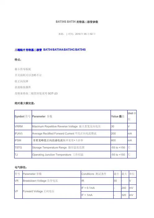
肖特基二极管参数表摘要:I.肖特基二极管简介A.肖特基二极管的定义B.肖特基二极管的作用II.肖特基二极管参数表A.肖特基二极管的分类B.肖特基二极管的主要参数1.最大重复峰值反向电压2.最大直流阻断电压3.最大正向平均整流电流4.最大瞬时正向电压5.最大直流反向电流C.肖特基二极管参数的重要性III.肖特基二极管参数的选择与应用A.参数选择的原则B.肖特基二极管的应用领域1.电源电路2.通信设备3.电子仪器4.其他领域IV.肖特基二极管的性能与使用寿命A.肖特基二极管的性能优势B.肖特基二极管的使用寿命C.提高肖特基二极管性能和使用寿命的方法正文:肖特基二极管是一种半导体器件,具有单向导通的特性,主要应用于电路中的整流、稳压、保护等场合。
它的参数表是选择和应用肖特基二极管的关键依据。
肖特基二极管参数表主要包括以下几个方面:1.最大重复峰值反向电压:指肖特基二极管能够承受的最大反向电压,决定了二极管在电路中工作的稳定性和可靠性。
2.最大直流阻断电压:肖特基二极管在正向导通状态下,能够承受的最大直流电压。
3.最大正向平均整流电流:肖特基二极管在正向导通状态下,能够承受的最大平均电流。
4.最大瞬时正向电压:指肖特基二极管在正向导通状态下,瞬时承受的最大正向电压。
5.最大直流反向电流:指肖特基二极管在反向截止状态下,能够承受的最大直流反向电流。
这些参数对于选择合适的肖特基二极管至关重要,关系到电路的正常工作和设备的安全。
在选择肖特基二极管参数时,需要根据具体应用场景和电路需求来进行权衡。
例如,对于电源电路,需要关注肖特基二极管的最大重复峰值反向电压和最大直流阻断电压;对于通信设备,需要关注其最大正向平均整流电流和最大瞬时正向电压;对于电子仪器,需要关注最大直流反向电流等参数。
肖特基二极管广泛应用于电源电路、通信设备、电子仪器等领域。
例如,在电源电路中,肖特基二极管可以实现整流、稳压等功能,保证电路的稳定运行;在通信设备中,肖特基二极管可以用于信号放大、开关等电路,提高通信质量和设备性能;在电子仪器中,肖特基二极管可以作为保护元件,防止电路因过电压、过电流等异常情况而受损。
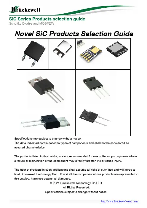
Schottky Diodes and MOSFETsNovel SiC Products Selection GuideSpecifications are subject to change without notice.The data indicated herein describe types of components and shall not be considered as assured characteristics.The products listed in this catalog are not recommended for use in life support systems where a failure or malfunction of the component may directly threaten life or cause injury.The user of products in such applications shall assume all risks of such use and will agree to hold Bruckewell Technology Co LTD and all the companies whose products are represented in this catalog, harmless against all damages.© 2021 Bruckewell Technology Co LTD.All Rights Reserved.Specifications subject to change without notice.Schottky Diodes and MOSFETsIn the recent decades, the Silicon carbide (SiC), turned out to be an excellent semiconductor material. Composed of carbon and silicon, and used in power applications in which it showed excellent performance,far superior to those of silicon.Significant progress has been made in the field of the semiconductor industry, in which the technologies forthe processing of silicon carbide have become increasingly more sophisticated, and have produced semiconductor devices with excellent performance.In the facts those devices during the applications have shown a remarkable capacity to reduce losses and ahigh switching speed in comparison to that offered by silicon. The use of silicon carbide (SiC) as a semiconductor begins to expand into multiple applications and always proves to be more and more the candidate to replace silicon in the most important applications such as automotive and E-Bike motor control.For these reasons, Bruckewell Semi decided to launch the production of the SiC Products, including the SiC Schottky Diode and SiC MOSFET, support the 650V to 1200V, and give the opportunity to its customers totake advantage of the benefits that the products offer in the SiC high-voltage power applications.Present our SiC products line as belowSMD PackageAmp DFN3X3 DFN5X6 TO-277 DFN 8X8 TO-252(DPak) TO-263(D2Pak)4 CBR04P65D6 CBR06P65HL CBR06P65D8 CBR08P65HL CBR08P65D10 CBR10P65HM CBR10P65SCBR10120SCBR10P65HLCBR10P65DCBR10120D20 CBR20120S30 CBR30120H CBR30120S40DFN 3X3 is unique package and CBR10P65HM is first smallest SiC SBD Diode in the industry.TO-277 has same foot print with TO-252 (DPak), and has better thermal performance.Through Hole PackageAmp TO-220AC TO-220AB TO-247 TO-247 (Dual Die)4 CBR04P656 CBR06P658 CBR08P6510 CBR10P65CBR10120 CBR10120PCBR10120W20 CBR20P65CBR20120CBR20P65PCCBR20120PCBR20P65WCBR20120WCBR20P65WCCBR20120WC30 CBR30120W40 CBR40P65WC CBR40120WCSchottky Diodes and MOSFETsPart NomenclatureExample: CBR20P65PC CBR SiC Barrier RectifierCMS SiC MOSFET20 IF, Forward current, as 20AP65 Breakdown Voltage, as P65=650V, 120=1200VPC Package CodeBlank: TO-220AC-2LP: TO-220ABPC: TO-220AB, Dual Die D: TO-252-2L, DPAKW: TO-247-2LWC: TO-247-3L, Dual Die WU: TO-247-3L, Single Die S: TO-277A: SMA, B: SMB, C: SMC B: TO-263, D2PAKH: DFN5x6HM: DFN3x3HL: DFN8x8When the diodes are used simultaneously:ΔTj(diode1) = P(diode1) x Rth(j-c) (per diode) + P(diode2) x Rth(c)To evaluate the conduction losses use the following equation:P = 1.35 x IF(AV) + 0.144 x IF2(RMS)Schottky Diodes and MOSFETsComparison with industry supplier-TO-220AC/ABAmpBruckewellST-MicroInfineonTO-220ACTO-220ABTO-220ACTO-220ABTO-220AC TO-220AB2 IDH02G65C5IDH02G120C53 IDH03SG60C IDH03G65C5 4CBR04P65IDH04SG60C IDH04G65C55 IDH05SG60C IDH05G65C5 IDH05G120C56 CBR06P65 STPSC6TH13TI IDH06SG60C IDH06G65C58 CBR08P65STPSC8TH13TI STPSC8H065CIDH08SG60C IDH08G65C5 IDH08G120C5 9IDH09SG60C IDH09G65C510CBR10P65 CBR10120CBR10120PSTPSC10H065D STPSC10H12D STPSC10TH13TIIDH10SG60CIDH10G65C5 IDH10G120C512 STPSC12065 STPSC1206 STPSC12H065CIDH12SG60C IDH12G65C515 STPSC15H1216STPSC16H065C IDH16G65C5IDH16G120C520CBR20P65 CBR20120CBR20P65PC CBR20120PSTPSC20065D STPSC20H12DSTPSC20H065CIDH20G65C5 IDH20G120C5Note:The suffix C5 in the Infineon Parts means the CoolSiC™ 5G, others are CoolSiC™ 3GSchottky Diodes and MOSFETsComparison with Japan suppliers-TO-220AC/ABAmpBruckewell Rohm Toshiba TO-220AC TO-220AB TO-220AC ITO-220AC TO-220AC ITO-220AC4 CBR04P65 SCS304AP TRS4E65F TRS4A65F5 SCS205KG6 CBR06P65 SCS306APSCS206AGSCS206AM TRS6E65F TRS6A65F8 CBR08P65 SCS308APSCS208AGSCS208AM TRS8E65F TRS8A65F10 CBR10P65CBR10120 CBR10120PSCS310APSCS210AGSCS210KGSCS210AM TRS10E65F TRS10A65F12 SCS212AG SCS212AM15 SCS215AGSCS215KGSCS215AM20 CBR20P65CBR20120CBR20P65PCCBR20120PSCS220AGSCS220KGSCS220AMNote:The suffix of Rohm Parts means the breakdown voltage, A means 650V, K means 1200VSchottky Diodes and MOSFETsComparison with industry supplier-TO-247 Single/ Dual DieAmpBruckewellST-MicroInfineonTO-247 TO-247 DualTO-247TO-247 DualTO-247TO-247 Dual 10 CBR10120WIDW10G65C5 IDW10G120C5B 20 CBR20P65W CBR20120W CBR20P65WC CBR20120WC STPSC20065WSTPSC20H065CWIDW20G65C5IDW20G65C5B IDW20G120C5B12 IDW12G65C515IDW15G120C5B16 IDW16G65C524IDW24G65C5B 30 CBR30120WIDW30G65C5IDW30G120C5B 32IDW32G65C5B 40CBR40120WCSTPSC40065CWIDW40G65C5IDW40G65C5B IDW40G120C5BComparison with Japan suppliers-TO-247 Single/ Dual DieAmpBruckewellRohmFuji electricTO-247 TO-247 DualTO-247TO-247 Dual TO-247 TO-247 Dual10 CBR10120WSCS210KE2FDCY10S6515SCS215AE20 CBR20P65W CBR20120W CBR20P65WC CBR20120WCSCS220AESCS220AE2 SCS220KE2FDCY18S120 FDCY20C6525 FDCY25S6530 CBR30120WSCS230AE2 SCS230KE240 CBR40120WCSCS240AE2 SCS240KE2FDCY36C120 50FDCY50C65Schottky Diodes and MOSFETsProduct IO(A)VB min (V)VF typ(V)IR Max (uA)PackageNumber of Diodes CBR04P65 4 650 1.5 10 TO-220AC 1 CBR04P65D 4 650 1.5 10 DPAK (TO-252) 1 CBR06P65 6 650 1.5 10 TO-220AC 1 CBR06P65D 6 650 1.5 10 DPAK (TO-252) 1 CBR 06P65HL 6 650 1.5 10 DFN 8X8 1 CBR08P65 8 650 1.5 10 TO-220AC 1 CBR08P65D 8 650 1.5 10 DPAK (TO-252) 1 CBR08P65HL 8 650 1.5 10 DFN 8X8 1 CBR10P65 10 650 1.5 10 TO-220AC 1 CBR10P65D 10 650 1.5 10 DPAK (TO-252) 1 CBR10P65S 10 650 1.5 10 TO-277 1 CBR10P65HM 10 650 1.5 10 DFN3.3 1 CBR10P65HL 10 650 1.5 10 DFN8X8 1 CBR20P65PC 20 650 1.5 10 TO-220AB 2 CBR20P65 20 650 1.5 10 TO-220AC 1 CBR20P65W 20 650 1.5 10 TO-247 1 CBR20P65WC 20 650 1.5 10 TO-247 2 CBR40P65WC 40 650 1.5 10 TO-247 2 CBR10120 10 1200 1.5 10 TO-220AC 1 CBR10120P 10 1200 1.5 10 TO-220AB 1 CBR10120D 10 1200 1.5 10 DPAK (TO-252) 1 CBR10120S 10 1200 1.5 10 TO-277 1 CBR10120W 10 1200 1.5 10 TO-247 1 CBR20120WC 20 1200 1.5 10 TO-247 2 CBR20120W 20 1200 1.5 10 TO-247 1 CBR20120 20 1200 1.5 10 TO-220AC 1 CBR20120P 20 1200 1.5 10 TO-220AB 1 CBR20120PC 20 1200 1.5 10 TO-220AB 2 CBR20120S 20 1200 1.5 10 TO-277 1 CBR30120W 30 1200 1.5 10 TO-247 1 CBR30120S 30 1200 1.5 10 TO-277 1 CBR30120H 30 1200 1.5 10 DFN 5X6 1 CBR40120WC 4012001.510 TO-2472Schottky Diodes and MOSFETsDisclaimerALL PRODUCT, PRODUCT SPECIFICATIONS AND DATA ARE SUBJECT TO CHANGE WITHOUT NOTICE TO IMPROVE RELIABILITY, FUNCTION OR DESIGN OR OTHERWISE. Bruckewell Technology Inc., its affiliates, agents, and employees, and all persons acting on its or their behalf (collectively, “Bruckewell”), disclaim any and all liability for any errors, inaccuracies or incompleteness contained in any datasheet or in any other disclosure relating to any product. Bruckewell makes no warranty, representation or guarantee regarding the suitability of the products for any particular purpose or the continuing production of any product. To the maximum extent permitted by applicable law, Bruckewell disclaims(i) Any and all liability arising out of the application or use of any product.(ii) Any and all liability, including without limitation special, consequential or incidental damages. (iii) Any and all implied warranties, including warranties of fitness for particular purpose, non-infringement and merchantability.Statements regarding the suitability of products for certain types of applications are based on Bruckewell’s knowledge of typical requirements that are often placed on Bruckewell products in generic applications.Such statements are not binding statements about the suitability of products for a particular application. It is the customer’s responsibility to validate that a particular product with the properties described in the product specification is suitable for use in a particular application. Parameters provided in datasheets and/or specifications may vary in different applications and performance may vary over time.Product specifications do not expand or otherwise modify Bruckewell’s terms and conditions of purchase, including but not limited to the warranty expressed therein.。
肖特基二极管手册肖特基二极管手册是一本介绍肖特基二极管的基础知识、特点、应用等方面的工具书,对于电子工程师和研究人员来说,是一本必不可少的参考书。
以下是本文对肖特基二极管手册内容进行的简要介绍。
第一部分:基础知识在这一部分中,手册介绍了肖特基二极管的基本原理,即该器件利用了金属-半导体接触的本质非对称性质,实现了非常优秀的整流效果。
手册中详细描述了金属-半导体界面的特殊结构和电学性质,以及该结构所带来的整流特性。
同时,肖特基二极管与传统的 P-N 结二极管相比,有着极高的速度和响应时间,以及低的噪声水平。
手册详细分析了这些特殊的性质,并且提供了实验数据和例子,以便读者更好地理解这些特点。
第二部分:特点和规格这一部分介绍了肖特基二极管的主要特征和规格参数。
手册详细解释了器件的最大可承受电压、额定电流和最大功率等特点,同时还介绍了其内部的各种特殊设计。
手册提供了非常详细和全面的指导和介绍,帮助读者了解如何选择和应用不同类型的肖特基二极管。
第三部分:应用在应用部分,手册介绍了肖特基二极管的实际应用和使用场景。
以 DC/DC 变换器、交流/直流转换器、折叠、调制和开关电源等器件为例,手册提供了一些不同应用领域的例子,说明了如何在特定的应用中选择和使用肖特基二极管。
同时,手册还介绍了一些实验和测试技术,以便读者更好地理解和掌握器件的特性和表现。
手册提供了多种实验方案和测试数据,帮助读者进行自己的实验和测试。
总结肖特基二极管手册是一本权威、全面、实用的工具书。
其中包含了肖特基二极管的基本知识、主要特点和规格、应用和实验方案等方面的信息,是一本值得电子工程师和研究人员深入阅读和掌握的参考书。
DATA SHEETProduct specificationSupersedes data of October 19931996Mar 19BAT54W seriesSchottky barrier (double) diodesook, halfpageM3D088Schottky barrier (double) diodes BAT54W seriesFEATURES•Low forward voltage•Guard ring protected•Very small SMD package.APPLICATIONS•Ultra high-speed switching •Voltage clamping•Protection circuits•Blocking diodes.DESCRIPTIONPlanar Schottky barrier diodes encapsulated in a SOT323 very small plastic SMD package. Single diodes and double diodes with different pinning are available.PINNINGPINBAT54W AW CW SW1a k1a1a12n.c.k2a2k23k a1,a2k1,k2k1,a 2Fig.1Simplified outline(SOT323) and pinconfiguration.handbook, 2 columns312MBC870Top viewFig.2BAT54W single diodeconfiguration (symbol).312n.c.MLC357Fig.3BAT54AW diodeconfiguration (symbol).312MLC360Fig.4BAT54CW diodeconfiguration (symbol).312MLC359Fig.5BAT54SW diodeconfiguration (symbol).312MLC358MARKINGTYPE NUMBER MARKING CODEBAT54W L4 BAT54AW42 BAT54CW43 BAT54SW44Schottky barrier (double) diodesBAT54W seriesLIMITING VALUESIn accordance with the Absolute Maximum Rating System (IEC 134).ELECTRICAL CHARACTERISTICS T amb =25°C unless otherwise specified.Note1.Pulsed test: t p =300µs;δ=0.02.THERMAL CHARACTERISTICS Note1.Refer to SOT323 standard mounting conditions.SYMBOL PARAMETERCONDITIONSMIN.MAX.UNITPer diode V R continuous reverse voltage −30V I F continuous forward current −200mA I FRM repetitive peak forward current t p ≤1s;δ≤0.5−300mA I FSM non-repetitive peak forward current t p <10ms −600mA P tot total power dissipation (per package)T amb ≤25°C−200mW T stg storage temperature −65+150°C T j junction temperature−125°C T amboperating ambient temperature−65+125°CSYMBOL PARAMETERCONDITIONSMAX.UNITPer diode V Fforward voltagesee Fig.6I F =0.1mA 240mV I F =1mA 320mV I F =10mA 400mV I F =30mA 500mV I F =100mA800mV I R reverse current V R =25V; note 1; see Fig.72µA t rrreverse recovery timewhen switched from I F =10mA to I R =10mA; R L =100Ω; measured at I R =1mA: see Fig.95nsC d diode capacitance f =1MHz; V R =1V; see Fig.810pFSYMBOL PARAMETERCONDITIONSVALUE UNIT R th j-a thermal resistance from junction to ambientnote 1625K/WSchottky barrier (double) diodesBAT54W seriesGRAPHICAL DATAhandbook, halfpage10I F V F (V)310(mA)21011011.20.80.40MSA892(3)(2)(1)(3)(2)(1)(1)T amb =125°C.(2)T amb =85°C.(3)T amb =25°C.Fig.6Forward current as a function of forward voltage; typical values.0102030V (V)R103I R(µA)102101101(1)(2)(3)MSA893(1)T amb =125°C.(2)T amb =85°C.(3)T amb =25°C.Fig.7Reverse current as a function of reverse voltage; typical values.010203051015V (V)RC d (pF)MSA891Fig.8Diode capacitance as a function of reversevoltage; typical values.f =1MHz; T amb =25°C.Fig.9 Reverse recovery definitions.handbook, halfpage 90%10%t fQ dI dttIFI RMRC129 - 1F rSchottky barrier (double) diodesBAT54W seriesPACKAGE OUTLINEDEFINITIONS LIFE SUPPORT APPLICATIONSThese products are not designed for use in life support appliances, devices, or systems where malfunction of these products can reasonably be expected to result in personal injury. Philips customers using or selling these products for use in such applications do so at their own risk and agree to fully indemnify Philips for any damages resulting from such improper use or sale.Data sheet status Objective specification This data sheet contains target or goal specifications for product development.Preliminary specification This data sheet contains preliminary data; supplementary data may be published later.Product specification This data sheet contains final product specifications.Limiting valuesLimiting values given are in accordance with the Absolute Maximum Rating System (IEC 134). Stress above one or more of the limiting values may cause permanent damage to the device. These are stress ratings only and operation of the device at these or at any other conditions above those given in the Characteristics sections of the specification is not implied. Exposure to limiting values for extended periods may affect device reliability.Application informationWhere application information is given, it is advisory and does not form part of the specification.handbook, full pagewidth0.250.10B0.20.2AAM M 1230.651.32.21.80.400.30B1.351.152.22.0detail XX1.1max0.10.01.00.80.30.10.2MBC871Dimensions in mm.Fig.10 SOT323.。
肖特基整流二极管型号及参数
肖特基整流二极管(Schottky Barrier Diode,简称SBD)是一种具有快速开关特性和低电压损耗的二极管。
其工作原理是通过形成金属和半导体之间的肖特基势垒来导电。
以下是一些常见的肖特基整流二极管型号及其参数介绍:
1.BAT54C:
-最大正向电流:600mA
-最大反向电压:30V
-正向压降:0.37V(I=0.1A)
- 导通时间:4ns
2.BAT46W:
-最大正向电流:150mA
-最大反向电压:100V
-正向压降:0.4V(I=0.1A)
- 导通时间:5ns
3.BAT41:
-最大正向电流:100mA
-最大反向电压:40V
-正向压降:0.45V(I=0.1A)
- 导通时间:8ns
4.BAT54S:
-最大正向电流:300mA
-最大反向电压:30V
-正向压降:0.26V(I=0.2A)
- 导通时间:6ns
5.BAT54:
-最大正向电流:600mA
-最大反向电压:30V
-正向压降:0.41V(I=0.1A)
- 导通时间:4ns
6.BAT85:
-最大正向电流:1A
-最大反向电压:30V
-正向压降:0.37V(I=0.1A)
- 导通时间:1ns
以上只是一些常用的肖特基整流二极管型号,实际上市场上还有很多其他型号的肖特基整流二极管。
不同型号的肖特基整流二极管具有不同的正向电流、反向电压、正向压降和导通时间等参数,可以根据具体应用需求选择合适的型号。
扬州扬杰肖特基二极管选型手册(最新版)目录1.扬州扬杰肖特基二极管选型手册概述2.扬州扬杰肖特基二极管的种类与特点3.扬州扬杰肖特基二极管的选型流程4.扬州扬杰肖特基二极管的应用领域5.结语正文一、扬州扬杰肖特基二极管选型手册概述扬州扬杰电子科技有限公司(以下简称“扬州扬杰”)致力于为客户提供高品质的半导体产品,其中肖特基二极管作为公司的主要产品之一,广泛应用于各种电子设备中。
为了帮助客户快速、准确地选择合适的肖特基二极管,扬州扬杰特别推出了肖特基二极管选型手册。
本手册旨在为客户提供详细的选型指导,确保客户能够根据实际需求选择到最佳的肖特基二极管。
二、扬州扬杰肖特基二极管的种类与特点1.种类扬州扬杰肖特基二极管分为多种类型,主要包括:(1)普通肖特基二极管(SBD)(2)快速恢复肖特基二极管(Fast Recovery SBD)(3)高电压肖特基二极管(High Voltage SBD)(4)低正向电压肖特基二极管(Low Forward Voltage SBD)扬州扬杰肖特基二极管具有以下特点:(1)低动态阻抗:在开关状态下,具有较低的动态阻抗,有利于提高整机效率。
(2)高电流速度:具有较高的电流速度,可满足高速开关需求。
(3)低正向电压:正向电压较低,有利于降低整机功耗。
(4)高抗浪涌能力:具有较高的抗浪涌能力,可有效保护电路免受浪涌冲击。
三、扬州扬杰肖特基二极管的选型流程1.确定需求参数:根据实际应用需求,确定所需的肖特基二极管参数,如正向电压、反向电压、电流、动态阻抗等。
2.对照产品手册:根据所需参数,查阅扬州扬杰肖特基二极管选型手册,初步筛选出符合要求的产品型号。
3.比较产品性能:对初步筛选出的产品型号进行性能比较,选择最符合需求的产品。
4.咨询专业技术支持:在选型过程中遇到问题,可随时联系扬州扬杰专业技术支持团队,获取专业建议。
四、扬州扬杰肖特基二极管的应用领域扬州扬杰肖特基二极管广泛应用于以下领域:1.通信设备:如手机、路由器、交换机等。
关于肖特基二极管、型号的命名、字母含义、解释肖特基二极管的命名:肖特基二极管是以其发明人肖特基博士(Schottky)命名的,完整的叫法是:肖特基整流二极管(Schottky Rectifier Diode缩写成SR),也有人叫做:肖特基势垒二极管(Schottky Barrier Diode缩写成SBD)的简称。
肖特基:Schottky整流:RectifierSR:即为肖特基整流二极管Schottky Rectifier Diode:肖特基整二极管,简称:SR,比如:SR107,SR10100CT......肖特基:Schottky势垒:BarrierSB:即为肖特基势垒二极管肖特基二极管也称肖特基势垒二极管(简称SBD),国内厂家也有叫做“SB1045CT、SR10100、SL....、BL....Schottky Barrier Diode:肖特基势垒二极管,简称:SB,比如:SB107,SB1045CT......Schottky Barrier Diode:也有简写为:SBD来命名产品型号前缀的。
但SBD不是利用P型半导体与N型半导体接触形成PN结原理制作的,而是利用金属与半导体接触形成的金属-半导体结原理制作的。
因此,SBD也称为金属-半导体(接触)二极管或表面势垒二极管,它是一种热载流子二极管。
关于肖特基MBR系列为什么国际通用常见的肖特基二极管都以“MBR”字头命名?因为最早是世界著名半导体公司-摩托罗拉半导体命名的产品型号M:是以最早MOTOROLA的命名,取MB:Bridge 桥;Barrier:势垒R:Rectifier,整流器 “MBR”意为整流器件SCHOTTKY:肖特基 SCHOTTKY RECTIFIER DIODES:肖特基整流二极管。
例如:MBR10200CTM:MOTOROLA 缩写MB:Barrier缩写BR:Rectifier 缩写R10:电流10A200:电压200VC:表示TO-220AB封装,常指半塑封。
常用的肖特基二极管型号及参数肖特基二极管是一种具有特殊结构的二极管,具有快速开关速度、低反向电流和低电压丢失的特点,广泛应用于电源管理、开关电源、高频电路、自增放大器、矩阵存储等领域。
下面是一些常见的肖特基二极管型号及其参数。
1.1N5711:1N5711是一种常用的肖特基二极管型号,其最大正向电流为15mA,最大反向电流为2uA,最大反向电压为70V。
2.BAT54:BAT54是一种超小型、超低电压丢失的肖特基二极管,其最大正向电流为600mA,最大反向电流为5uA,最大反向电压为30V。
该型号适用于电源管理、无线通信、自增放大器等应用领域。
3.BAS70:BAS70是一种超小型、超低电压丢失、低反向电流的肖特基二极管,其最大正向电流为70mA,最大反向电流为50nA,最大反向电压为70V。
该型号适用于电源管理、高频电路、模拟开关等领域。
4.1N5819:1N5819是一种经典的肖特基二极管型号,其最大正向电流为1A,最大反向电流为5uA,最大反向电压为40V。
该型号适用于开关电源、充电器、汽车电路等应用领域。
5.SB520:SB520是一种超速肖特基二极管,其最大正向电流为5A,最大反向电流为5uA,最大反向电压为20V。
该型号适用于变换器、电源管理、DC/DC转换器等高功率应用领域。
6.SR240:SR240是一种高速肖特基二极管,其最大正向电流为2A,最大反向电流为5uA,最大反向电压为40V。
该型号适用于开关电源、电机驱动、变换器等高速开关应用领域。
以上只是常见的一些肖特基二极管型号及其参数,不同型号的肖特基二极管在正向电流、反向电流和反向电压等参数上存在差异。
在实际选择时,需要根据具体应用场景和要求来选择合适的肖特基二极管型号。
关于肖特基二极管、型号的命名、字母含义、解释肖特基二极管的命名:肖特基二极管是以其发明人肖特基博士(Schottky)命名的,完整的叫法是:肖特基整流二极管(Schottky Rectifier Diode缩写成SR),也有人叫做:肖特基势垒二极管(Schottky Barrier Diode缩写成SBD)的简称。
肖特基:Schottky整流:RectifierSR:即为肖特基整流二极管Schottky Rectifier Diode:肖特基整二极管,简称:SR,比如:SR107,SR10100CT......肖特基:Schottky势垒:BarrierSB:即为肖特基势垒二极管肖特基二极管也称肖特基势垒二极管(简称SBD),国内厂家也有叫做“SB1045CT、SR10100、SL....、BL....Schottky Barrier Diode:肖特基势垒二极管,简称:SB,比如:SB107,SB1045CT......Schottky Barrier Diode:也有简写为:SBD来命名产品型号前缀的。
但SBD不是利用P型半导体与N型半导体接触形成PN结原理制作的,而是利用金属与半导体接触形成的金属-半导体结原理制作的。
因此,SBD也称为金属-半导体(接触)二极管或表面势垒二极管,它是一种热载流子二极管。
关于肖特基MBR系列为什么国际通用常见的肖特基二极管都以“MBR”字头命名?因为最早是世界著名半导体公司-摩托罗拉半导体命名的产品型号M:是以最早MOTOROLA的命名,取MB:Bridge 桥;Barrier:势垒R:Rectifier,整流器 “MBR”意为整流器件SCHOTTKY:肖特基 SCHOTTKY RECTIFIER DIODES:肖特基整流二极管。
例如:MBR10200CTM:MOTOROLA 缩写MB:Barrier缩写BR:Rectifier 缩写R10:电流10A200:电压200VC:表示TO-220AB封装,常指半塑封。
一文详解肖特基二极管和PN结二极管的选型二极管选型相对简单,相信每个硬件工程师,都有对比过肖特基二极管与PN结二极管的差异。
差异无非有以下结果:表中参数,看看就好,并不严格,知道二者之间的相对大小就行了。
了解了上面参数,基本就知道什么电路,该选什么类型的二极管了。
能用PN结二极管的地方就用PN结二极管,因为价格便宜。
肖特基二极管的优势主要在速度和压降,对这两个没要求的场景,那自然选择更便宜的由PN结构成的二极管。
下面说个在实际工作中可能忽视的点。
二极管导通电压提起二极管导通电压,估计脑子里面都是0.7V,形成这个印象其实并不好,有4点原因。
1、这个0.7V,说的是PN结二极管,肖特基二极管要更低。
我们经常使用二极管串联在电源支路上面,防止倒灌。
那你担心过二极管上面压降太大吗?其实你可能没有注意,在对压降有要求的地方,可能用的就是肖特基二极管,它的压降有多低呢?以BAT60BE237为例子吧,截个图给大家看看。
你看,通过10mA的电流,压降才0.24V。
对于一些小电流防倒灌的场合,电压不能下降太多,肖特基二极管就比较实用了。
如果工作电流更小,可能压降才零点一几伏。
所以,不要看到个电路中串了个二极管,就觉得这个压降是0.7V。
2、导通电压门限,这本身就是个模糊的定义。
我们知道二极管的伏安特性曲线是对数关系,那到底是通过1mA电流时看作开始导通,还是10mA100mA?3、导通电压有时会到1V以上,不同型号也相差比较大。
总会有用到大电流的时候,其实也不用太大,1A就行。
这时PN结构成的二极管,它导通电压其实一般都到1V左右了。
下图是超快恢复二极管,可以看到1A时,导通电压在1V以上,其中耐压600V以上的二极管导通电压都到了1.7V。
你还要说导通电压是0.7V吗?4、发光二极管导通压降差异更大o4YBAGCWXYeAP26ZAADT_CHT0YI484.png发光二极管也是二极管,不过它的区别就更大了。