飞思卡尔推出全新的工业加速度传感器
- 格式:pdf
- 大小:224.39 KB
- 文档页数:4

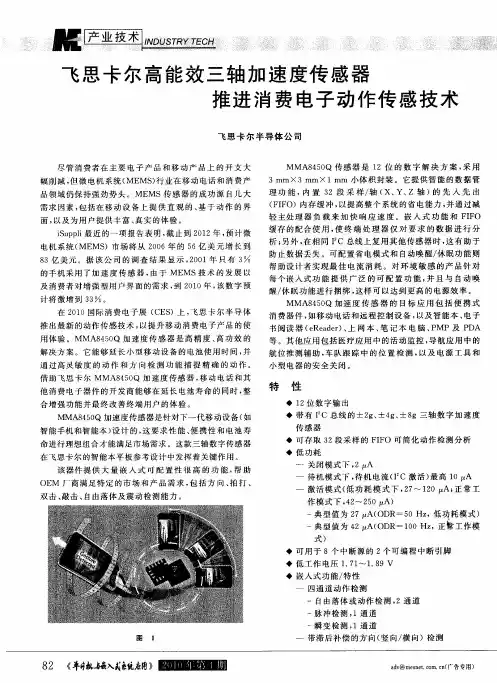
飞思卡尔半导体推出3款敏感度极高的传感器
佚名
【期刊名称】《机电一体化》
【年(卷),期】2006(12)5
【摘要】飞思卡尔半导体(Freescale)日前推出3款敏感度极高的传感器,即MEMS的MMA6270Q(XY轴)、MMA6280Q(XZ轴)和MMA7261Q (XYZ轴)传感器(也称为加速计)。
【总页数】1页(P58-58)
【关键词】传感器;敏感度;半导体;卡尔;MEMS;加速计;Z轴
【正文语种】中文
【中图分类】TH-39
【相关文献】
1.飞思卡尔:变中求“胜”——专访飞思卡尔半导体董事会主席兼CEO Rich Beyer 先生 [J], 于寅虎
2.飞思卡尔半导体技术园地飞思卡尔降低联网市场千兆以太网成本 [J],
3.飞思卡尔:以持续创新和中国共赢——访飞思卡尔半导体高级副总裁兼亚洲区总经理姚天从先生 [J], 胡芃
4.飞思卡尔推出三款高敏感度传感器 [J],
5.飞思卡尔Flexis JM控制器系列灵活启动USB连接的开发飞思卡尔半导体(中国)有限公司 [J],
因版权原因,仅展示原文概要,查看原文内容请购买。
© 2010, 2012 Freescale Semiconductor, Inc. All rights reserved.Document Number: AN4074Rev 1, 03/2012Freescale Semiconductor Application NoteAuto-Wake/Sleep Using the MMA8451, 2, 3Qby: Kimberly TuckApplications Engineer1.0IntroductionAccelerometers are commonly used in hand-held electronics and/or battery operated electronic devices.Consumption of current in the entire system is a critical feature of the product design. Users do not want to be inconvenienced by continually recharging or changing out batteries. When designing in the accelerometer, battery power usage is often a critical feature which concerns many designers.Therefore, current consumption of the sensor as well as of the entire system should be paramount design considerations. If the system processor is used often only for processing data from the accelerometer, then it is ideal to embed the intelligence in the sensor to avoid burdening the system processor from running continually. The flexibility ofembedded interrupt driven functions and selectable data rates with trade-offs for resolution, response time, and current are the types of intelligent features in the MMA8451, 2, 3Q.This application note will explain the following:•The Auto-Wake/Sleep feature•Description of the configuration procedure withexample register settings and code.1.1Key WordsAccelerometer, Output Data Rate (ODR), Current, Standby Current, Power Down Mode Current, Low Power Mode, Noise, Auto-Wake/Sleep, Sleep Timer, Sensor.TABLE OF CONTENTS1.0 Introduction . . . . . . . . . . . . . . . . . . . . . . . . . . . . . . . . . . . . . . . . . . . . . . . . .11.1 Key Words . . . . . . . . . . . . . . . . . . . . . . . . . . . . . . . . . . . . . . . . . . . . . . . . . . .11.2 Summary . . . . . . . . . . . . . . . . . . . . . . . . . . . . . . . . . . . . . . . . . . . . . . . . . . . .22.0 MMA8451, 2, 3Q Consumer 3-axis Accelerometer 3 by 3 by 1 mm. . . . .22.1 Output Data, Sample Rates and Dynamic Ranges of all Three Products . . .22.1.1 MMA8451Q . . . . . . . . . . . . . . . . . . . . . . . . . . . . . . . . . . . . . . . . . . . . . .22.1.2 MMA8452Q . . . . . . . . . . . . . . . . . . . . . . . . . . . . . . . . . . . . . . . . . . . . . .22.1.3 MMA8453Q Note: No HPF Data . . . . . . . . . . . . . . . . . . . . . . . . . . . . . . .23.0 Configuring the MMA8451, 2, 3Q into Auto-Wake/Sleep Mode . . . . . . . .33.1 Set the Sleep Enable Bit . . . . . . . . . . . . . . . . . . . . . . . . . . . . . . . . . . . . . . . . .43.2 Set the Sleep Mode and Wake Mode Oversampling Mode. . . . . . . . . . . . . . .43.3 Configure the Sleep Sample Rate and Wake Sample Rate . . . . . . . . . . . . . .53.4 Set the Timeout Counter . . . . . . . . . . . . . . . . . . . . . . . . . . . . . . . . . . . . . . . . .53.5 Enable the Interrupts to be used in the System and Route to INT1 or INT2. . . . . . . . . . . . . . . . . . . . . . . . . . . . . . . . . . . . . . . . . . . . . . . . . . . . . . . . . . . .63.6 Enable the Interrupt Sources that Wake the Device . . . . . . . . . . . . . . . . . . . .64.0 Example Configuration for the Auto-Wake/Sleep Function. . . . . . . . . . .7Table 14.Registers used for Auto-Wake/Sleep Functionality. . . . . . . . . . . . . . . .74.1 Example Procedure for Configuring the Auto-Wake/Sleep Function Conditions. . . . . . . . . . . . . . . . . . . . . . . . . . . . . . . . . . . . . . . . . . . . . . . . . . . . . . . . . . . .8AN4074Sensors1.2SummaryThe MMA845xQ can be used to cycle between different ODRs, which results in overall lower current consumption of the device. This can be achieved from several programmable functions.2.0MMA8451, 2, 3Q Consumer 3-axis Accelerometer 3 by 3 by 1 mmThe MMA8451, 2, 3Q has a selectable dynamic range of ±2g, ±4g, ±8g. The device has 8 different output data rates, selectable high pass filter cut-off frequencies, and high pass filtered data. The available resolution of the data and the embedded features is dependant on the specific device.Note: The MMA8450Q has a different memory map and has a slightly different pinout configuration.Figure 1. MMA8451, 2, 3Q Consumer 3-axis Accelerometer 3 by 3 by 1 mm2.1Output Data, Sample Rates and Dynamic Ranges of all Three Products2.1.1MMA8451Q1.14-bit data2g (4096 counts/g = 0.25 mg/LSB) 4g (2048 counts/g = 0.5 mg/LSB) 8g (1024 counts/g = 1 mg/LSB)2.8-bit data2g (64 counts/g = 15.6 mg/LSB) 4g (32 counts/g = 31.25 mg/LSB) 8g (16 counts/g = 62.5 mg/LSB)3.Embedded 32 sample FIFO (MMA8451Q)2.1.2MMA8452Q1.12-bit data2g (1024 counts/g = 1 mg/LSB) 4g (512 counts/g = 2 mg/LSB) 8g (256 counts/g = 3.9 mg/LSB)2.8-bit data2g (64 counts/g = 15.6 mg/LSB) 4g (32 counts/g = 31.25 mg/LSB) 8g (16 counts/g = 62.5 mg/LSB)2.1.3MMA8453Q Note: No HPF Data1.10-bit data2g (256 counts/g = 3.9 mg/LSB) 4g (128 counts/g = 7.8 mg/LSB) 8g (64 counts/g = 15.6 mg/LSB)2.8-bit data2g (64 counts/g = 15.6 mg/LSB) 4g (32 counts/g = 31.25 mg/LSB) 8g(16 counts/g = 62.5 mg/LSB)12345910111213141516876N CV D DN CVDDIO BYP NC SCL GNDNC GND INT1GND INT2S A 0N CS D AMMA845xQ 16-Pin QFN (Top View)AN4074Sensors3.0Configuring the MMA8451, 2, 3Q into Auto-Wake/Sleep ModeThe MMA8451, 2, 3Q can be configured to transition between different sample rates (different current consumption) based on different selected events. Enabling this feature can be accomplished by enabling the Sleep Mode and setting a timeout period. Then the functions of interest must be set to trigger the device to wake. Both Wake and Sleep are considered “Active” Modes because data and interrupts are available. The difference between the modes is that the sample rate in Sleep Mode is limited to a maximum of 50 Hz. The advantage of using the Auto-Wake/Sleep is that the system can automatically transition to a higher sample rate (higher current consumption) when needed but spends the majority of the time in the Sleep Mode (lower current) when the device does not require higher sampling rates. This can all be triggered on selected events. The Low Noise bit (Register 0x2A bit 2) can be used as well with this feature. Be aware that using the Low Noise bit will limit the dynamic range to 4g, regardless of the set range of the full scale value. The oversampling mode can also be changed from Active Sleep Mode to Active Wake Mode. The Sleep Mode oversampling option is set in Register 0x2B using bit 3 and bit 4 SMODS0 and SMODS1. The Active Wake Mode oversampling option is set in Register 0x2B using bit 0 and bit 1 MODS0 and MODS1. For example the device can be configured to be in Low Power Mode when asleep at 1.56 Hz to be in the lowest current consumption configuration. Then the device can be set for High Resolution Mode at 6.25 Hz when awake to be prepared to take higher resolution data for a tilt application.Figure 2 shows transition states from the Wake, Sleep and Standby modes.Figure 2. Mode TransitionsTable 1 compares how the current consumption changes with the data rate and with the oversampling mode chosen. The over-sampling modes are “Normal”, “Low Noise and Low Power”, “High Resolution” and “Low Power”. The oversampling ratios are given at each data rate along with the current consumption values for each. The more averaging done internally results in higher current consumption. Note the Low Power Mode has the least amount of averaging and the lowest current consumption.Table 2 shows the list of functions that will delay the device from returning to sleep and waking from sleep. Note that the MMA8451Q is the only device that contains the FIFO. The FIFO can delay the device from going to sleep but it is not capable of waking the device from sleep. The transient, portrait/landscape, tap, and motion/freefall functions can all delay the device from sleep by servicing the interrupt before the timeout period. They can also wake the device from sleep. The Auto-Sleep interrupt indicates when the device changes modes from Wake to Sleep or Sleep to Wake but the interrupt does not affect the state change. Also the data ready interrupt does not affect the state change from the Wake to Sleep or Sleep to Wake state.Table 1. (S)MODS Oversampling Options with Current Consumption ValuesMode ODR NormalLow Noise and Low Power High Resolution Low PowerCurrent μAOS RatioCurrent μAOS RatioCurrent μAOS RatioCurrent μAOSRatio8001652165216521652400165416541654852200854854165844210044444416516242502442441653214212.5241684165128626.25243288165256641.5625241288321651024616StandbySYSMOD[1:0] = 00WakeSYSMOD[1:0] = 01<DR>SleepSYSMOD[1:0] = 10A SLP_RATE[1:0]I n t e r r u p t s If Time > ASLP_COUNT[7:0] and no Interrupts triggeredt r i g g e r e dAN4074SensorsNote that to configure the Auto-Wake/Sleep functionality, the selected embedded functions must be enabled (Register 0x2D) and the same corresponding functions must be set to “Wake-from-Sleep” (Register 0x2C) if they are to be used to wake the de-vice.All enabled functions will still function in Sleep Mode at the sleep ODR. Only the functions that have been selected for “Wake-from-Sleep” will wake the device. If nothing is selected to Wake-from-Sleep then the device will remain in Sleep Mode and will never wake up.This section reviews the different registers involved in configuring the device for auto-wake/sleep.1.Register 0x2B bit 2 – SLPE Enable Sleep bit2.Register 0x2B Set the Sleep Mode Oversampling Rate3.Register 0x2A Sleep Sample Rate and Wake Sample Rate4.Register 0x29 Timeout Counter5.Register 0x2D Enable the Interrupts for the Selected Functions6.Register 0x2E Route the Interrupts to INT1 or INT27.Register 0x2C Enable the Wake-from-Sleep Interrupts3.1Set the Sleep Enable BitIf the Sleep Enable bit (Register 0x2B bit 2) is NOT enabled then the device can only toggle between Standby and Wake Mode by writing to the Active bit in Register 0x2A. When the Sleep Enable bit is enabled the device can transition between Standby, Wake, and Sleep. The SLPE bit is shown as bit 2 in Table 4.3.2Set the Sleep Mode and Wake Mode Oversampling ModeThere are four different oversampling modes described in Table 3 They are “Normal”, “Low Noise and Low Power”, “High Res-olution” and “Low Power”. The oversampling mode changes the current consumption, resolution and also the debounce counter timers in the part. The device can be configured to be in Low Power Mode while in Sleep and then to Normal Mode when awake or any of the other fifteen combinations. This allows for further current savings in the Sleep Mode. The different bit settings are shown in Table 3. The Wake oversampling modes configured from bit 0 and bit 1 in Register 0x2B. The Sleep oversampling modes are configured from bit 3 and bit 4 in SMODS in Register 0x2B.Table 2. Interrupt Sources and the effects on the state change from Wake to Sleep and Sleep to Wake ModesInterrupt Source Event Restarts Timer and Delays Return-to-SleepEvent will Wake-from-SleepFIFO_GATE Yes No SRC_TRANS Yes Yes SRC_LNDPRT Yes Yes SRC_PULSE Yes Yes SRC_FF_MT Yes Yes SRC_ASLP No No SRC_DRDYNoNoTable 3. Settings for Oversampling Modes(S)MODS1(S)MODS0Power Mode 00Normal01Low Noise and Low Power10High Resolution 11Low PowerTable 4. 0x2B CTRL_REG2 Register (Read/Write) and DescriptionBit 7Bit 6Bit 5Bit 4Bit 3Bit 2Bit 1Bit 0STRSTSMODS1SMODS0SLPEMODS1MODS03.3Configure the Sleep Sample Rate and Wake Sample RateIt is important to note that when the device is in Sleep Mode, the system ODR is overwritten by the data rate set by the ASLP_RATE field in the CTRL_REG1 Register (0x2A). The Sleep Sample Rate (ASLP_RATE[0:1]) and the Wake Mode Sample Rate (DR[0:3]) are found in Table 5. The different bit settings for the Sleep Mode Sample Rate can be found in Table 6. The bit settings for the Wake Mode Sample Rates are found in Table 7.Table 5. 0x2A CTRL_REG1 Register (Read/Write) and DescriptionBit 7Bit 6Bit 5Bit 4Bit 3Bit 2Bit 1Bit 0 ASLP_RA TE1ASLP_RA TE0DR2DR1DR0LNOISE F_READ ACTIVETable 6. Sleep Mode Sample Rate DescriptionASLP_RATE1ASLP_RATE0ODR Period0050 Hz20 ms0112.5 Hz80 ms10 6.25 Hz160 ms11 1.56 Hz640 msTable 7. Wake Mode Sample Rate DescriptionDR2DR1DR0ODR Period000800.0 Hz 1.25 ms001400.0 Hz 2.5 ms010200.0 Hz 5 ms011100.0 Hz10 ms10050.0 Hz20 ms10112.5 Hz80 ms110 6.25 Hz160 ms111 1.56 Hz640 ms3.4Set the Timeout CounterThe ASLP_COUNT Register 0x29 shown in Table 8 sets the minimum time period of inactivity required to change the current ODR value from the value specified in the DR[2:0] to that in the ASLP_RATE[1:0] (Register 0x2A). Of course this only occurs provided the SLPE bit is set.Table 8. 0x29 ASLP_COUNT Register (Read/Write) and DescriptionBit 7Bit 6Bit 5Bit 4Bit 3Bit 2Bit 1Bit 0 D7D6D5D4D3D2D1D0 D7-D0 defines the minimum duration time to change current ODR value from DR to ASLP_RATE. Time step and maximum value depend on the ODR chosen. See Table 9.Table 9. ASLP_COUNT Relationship with ODROutput Data Rate (ODR)Duration ODR Time Step ASLP_COUNT Step8000 to 81s 1.25 ms320 ms4000 to 81s 2.5 ms320 ms2000 to 81s 5 ms320 ms1000 to 81s10 ms320 ms500 to 81s20 ms320 ms12.50 to 81s80 ms320 ms6.250 to 81s160 ms320 ms1.560 to 162s640 ms640 msAN4074 SensorsAN4074Sensors3.5Enable the Interrupts to be used in the System and Route to INT1 or INT2The interrupt functions must be enabled in Register 0x2D per Table 10 for the event to trigger the Auto-Wake/Sleep. The func-tions must also be configured with the appropriate thresholds and timing values to detect the events.The corresponding interrupt enable bit allows the function to route its event detection flag to the interrupt controller. The inter-rupt controller routes the enabled interrupt to the INT1 or INT2 pin. By default all interrupts are routed to INT2 and the correspond-ing configuration register bit value is 0. To route a functional block to INT1 instead of the default, set the corresponding configuration register bit to 1. The configuration register bit settings are shown in Table 11.3.6Enable the Interrupt Sources that Wake the DeviceThe register to control which interrupts will wake the device are configured in Register 0x2C shown in Table 12. There are five (5) functions that can be used to keep the sensor from falling asleep if they are enabled. These are the Transient, Orien-tation, Tap, Motion/FF and the FIFO. There are only four (4) functions used to wake the device. The FIFO will not wake the device from sleep. Also note the Auto-Wake/Sleep interrupt and the data ready interrupt do not affect the Wake/Sleep. Note that the FIFO is only available in the MMA8451Q device.Note: The FIFO is flushed whenever the system ODR changes in order to prevent mixing the FIFO data from different time domains unless the FIFO_GATE (bit 7) is set. Also, the FIFO cannot wake the device from sleep but can prevent the device from going to sleep. Details of the functionality of the FIFO is captured in Table 13.Table 10. Register 0x2D CTRL_REG4 Register (Read/Write) and DescriptionBit 7Bit 6Bit 5Bit 4Bit 3Bit 2Bit 1Bit 0INT_EN_ASLPINT_EN_FIFOINT_EN_TRANSINT_EN_LNDPRTINT_EN_PULSEINT_EN_FF_MT—INT_EN_DRDYTable 11. Register 0x2E CTRL_REG5 Register (Read/Write) and DescriptionBit 7Bit 6Bit 5Bit 4Bit 3Bit 2Bit 1Bit 0INT_CFG_ASLPINT_CFG_FIFOINT_CFG_TRANS INT_CFG_LNDPRT INT_CFG_PULSE INT_CFG_FF_MT—INT_CFG_DRDYTable 12. Register 0x2C CTRL_REG3 Interrupt Control Register and DescriptionBit 7Bit 6Bit 5Bit 4Bit 3Bit 2Bit 1Bit 0FIFO_GA TEWAKE_TRANS WAKE_LNDPRT WAKE_PULSEWAKE_FF_MT—IPOLPP_ODTable 13. Behavior of FIFO under Wake/Sleep ConditionsFIFO INT EnabledWake-from-SleepEnabledResultNO NOFIFO will fall asleep when the sleep timer times out and no other interrupt wakes the system.There is an AUTOMATIC flush and the FIFO starts refilling at the Sleep ODR from 0.If another functional block causes the device to wake the FIFO will FLUSH itself again and start filling at the Wake ODR.YES NOWith the interrupt enabled the FIFO can be read and flushed clearing the interrupt. The system is kept from falling asleep by reading the status after the interrupt is set. The FIFO does not have to be flushed to keep the device in Wake Mode- as long as the FIFO status is read continuously after the FIFO interrupt is enabled. If the system falls asleep (and no new interrupts occur during the timeout period), the FIFO AUTOMATICALLY flushes and starts refilling at the Sleep ODR from 0 and stores at the Wake ODR.NO YESFIFO will fall asleep if no wake events occur within the timeout st data remains here in the FIFO until it is flushed.Once the FIFO is flushed, it will start collecting the new data at the current ODR.YES YESWith interrupt enabled, the FIFO can be read and flushed (clearing the interrupt) . Note: Reading the FIFO status will keep the system from falling asleep.If the system does fall asleep (and no interrupts occur during the timeout period) then the FIFO will stop collecting any data. The last data will be held in the FIFO.Once the FIFO is flushed, it will start collecting the new data at the current ODR.AN4074Sensors4.0Example Configuration for the Auto-Wake/Sleep FunctionThe following are the steps to configure the Auto-Wake/Sleep function with the registers of importance in Table 14. In this ex-ample, the data rate will be set to 100 Hz in Wake Mode and 6.25 Hz in Sleep Mode. The Oversampling Mode will be set to High Resolution in the Wake Mode and Low Power Mode in Sleep Mode. The timeout period will be set to 20 seconds. The wake triggers will be tap and motion. There may be other interrupts that are enabled in the system including orientation detection, but these will not wake the device in this example.Table 14. Registers used for Auto-Wake/Sleep FunctionalityReg Name Definition Bit 7Bit 6Bit 5Bit 4Bit 3Bit 2Bit 1Bit 00B SYSMOD System ModeR FGERR FGT_4FGT_3FGT_2FGT_1FGT_0SYSMOD1SYSMOD00C INT_SOURCE Interrupt StatusR SRC_ASLPSRC_FIFOSRC_TRANSSRC_LNDPRTSRC_PULSESRC_FF_MT—SRC_DRDY29ASLP_COUNT Auto-Sleep CounterR/W D7D6D5D4D3D2D1D02A CTRL_REG1Control Reg1R/W ASLP_RATE1ASLP_RATE0DR2DR1DR0LNOISE F_READ ACTIVE 2BCTRL_REG2Control Reg2R/W STRSTSMODS1SMODS0SLPEMODS1MODS02C CTRL_REG3Control Reg3R/W(Wake Interrupts fromSleep)FIFO_GATE WAKE_TRANS WAKE_LNDPRT WAKE_PULSE WAKE_FF_MT —IPOL PP_OD2D CTRL_REG4Control Reg4R/W(Interrupt Enable Map)INT_EN_ASLP INT_EN_FIFO INT_EN_TRANS INT_EN_LNDPRT INT_EN_PULSE INT_EN_FF_MT —INT_EN_DRDY2E CTRL_REG5Control Reg5R/W(Interrupt Configuration)INT_CFG_ASLP INT_CFG_FIFO INT_CFG_TRANS INT_CFG_LNDPRT INT_CFG_PULSE INT_CFG_FF_MT —INT_CFG_DRDY4.1Example Procedure for Configuring the Auto-Wake/Sleep Function Conditions•Dynamic Range = 2g•Sleep Timeout period = 20 seconds•Wake Triggers = Tap and Motion•Wake Sample Rate = 100 Hz,•Wake Oversampling Mode = High Resolution•Sleep Sample Rate = 6.25 Hz•Sleep Oversampling Mode = Low PowerStep 1:Put the device in Standby ModeRegister 0x2A CTRL_REG1CTRL_REG1_Data = IIC_RegRead(0x2A);CTRL_REG1_Data& = 0xFE; //Clear Active BitIIC_RegWrite(0x2A,CTRL_REG1_Data);Step 2:To enable the Auto-Wake/Sleep set bit 2 in Register 0x2B, the SLPE bit.Register 0x2B CTRL_REG2CTRL_REG2_Data = IIC_RegRead(0x2B); //Store value in the RegisterCTRL_REG2_Data| = 0x04; //Set the Sleep Enable bitIIC_RegWrite(0x2B, CTRL_REG2_Data); //Write the updated value into CTRL_REG2.Step 3:The sleep sample rate must be chosen by writing in the corresponding sample rate value to bits6 and7 ASLP_RATE0 and ASLP_RATE1 (01) and the Wake Sample rate bits 5, 4 and 3 to DR(011) in Register 0x2A.Register 0x2A CTRL_REG1 ASLP_RATE = 01 (6.25 Hz), DR = 011(100 Hz)CTRL_REG1_Data = IIC_RegRead(0x2A);CTRL_REG1_Data& = 0x5E; //clear the bits that should be cleared for the sample ratesCTRL_REG1_Data| = 0x58; //Set ASLP = 6.25 Hz, DR = 100 HzIIC_RegWrite(0x2A,CTRL_REG1_Data);Step 4:Set the Wake Oversampling Mode to High Resolution (10) and the Sleep Oversampling Mode to Low Power (11)CTRL_REG2_Data = IIC_RegRead(0x2B);CTRL_REG2_Data& = 0xE4; //puts both Oversampling modes in Normal ModeCTRL_REG2_Data| = 0x1A; //Wake High Res, Sleep Low PowerIIC_RegWrite(0x2B,CTRL_REG2_Data);Step 5:The Interrupt for the event to trigger the device to wake up must be enabled by writing to Register 0x2D, CTRL_Reg4. Bits 2 through 7 will affect the Auto-Wake/sleep. The data readyinterrupt doesn’t trigger the Auto-Wake/Sleep mechanism.Example: Set Pulse and Orientation and Motion 1 and Auto-Wake/Sleep InterruptsEnabled in the SystemIIC_RegWrite(0x2D, 0x9C);Step 6:Route the interrupt chosen and enabled to either INT1 or INT2 in Register 0x2E CTRL_REG5.Example: Route Pulse, Motion1 and Orientation to INT2 and Auto-Sleep to INT1.IIC_RegWrite(0x2E,0x80);Step 7:Enable the interrupts that will wake the device from sleep. There can be more interrupts enabled in Step 4 than in Step 6. Only interrupts that are Enabled in Step 4 and that have the “Wake-from-Sleep” bit set in Register 0x2C will actually wake the device.Example: Choose Pulse and Motion to wake the device from sleepIIC_RegWrite(0x2C,0x18);AN4074SensorsStep 8:Set the Dynamic Range to 2gRegister 0x0E XYZ_DATA_CFGXYZ_CFG_Data = IIC_RegRead(0x0E);XYZ_CFG_Data & = 0xFC; //Clear the FS bits to 00 2gIIC_RegWrite(0x0E, XYZ_CFG_Data);Step 9:Write an Interrupt Service routine to monitor the Auto-Sleep InterruptInterrupt void isr_KBI (void){//clear the interrupt flagCLEAR_KBI_INTERRUPT;//Determine the source of interrupt by reading the system interrupt registerInt_SourceSystem = IIC_RegRead(0x0C);//Set up Case statement here to service all of the possible interruptsif ((Int_SourceSystem &=0x80)==0x80){//Perform an Action since Auto-Sleep Flag has been set//Read the System Mode to clear the system interruptInt_SysMod = IIC_RegRead(0x0B);if (Int_SysMod==0x02){//sleep mode}else if (Int_SysMod==0x01){//Wake Mode}else{//Error}}}Related DocumentationThe MMA845xQ device features and operations are described in a variety of reference manuals, user guides, and application notes. To find the most-current versions of these documents:1.Go to the Freescale homepage at:/2.In the Keyword search box at the top of the page, enter the device number MMA845xQ.3.In the Refine Your Result pane on the left, click on the Documentation link.AN4074 SensorsHow to Reach Us:Home Page:Web Support:/supportUSA/Europe or Locations Not Listed: Freescale Semiconductor, Inc. Technical Information Center, EL516 2100 East Elliot RoadTempe, Arizona 852841-800-521-6274 or +1-480-768-2130 /supportEurope, Middle East, and Africa:Freescale Halbleiter Deutschland GmbHTechnical Information CenterSchatzbogen 781829 Muenchen, Germany+44 1296 380 456 (English)+46 8 52200080 (English)+49 89 92103 559 (German)+33 1 69 35 48 48 (French)/supportJapan:Freescale Semiconductor Japan Ltd.HeadquartersARCO Tower 15F1-8-1, Shimo-Meguro, Meguro-ku,Tokyo 153-0064Japan0120 191014 or +81 3 5437 9125support.japan@Asia/Pacific:Freescale Semiconductor China Ltd.Exchange Building 23FNo. 118 Jianguo RoadChaoyang DistrictBeijing 100022China+86 10 5879 8000@For Literature Requests Only:Freescale Semiconductor Literature Distribution Center 1-800-441-2447 or +1-303-675-2140Fax: +1-303-675-2150 LDCForFreescaleSemiconductor@AN4074Information in this document is provided solely to enable system and software implementers to use Freescale Semiconductor products. There are no express or implied copyright licenses granted hereunder to design or fabricate any integrated circuits or integrated circuits based on the information in this document.Freescale Semiconductor reserves the right to make changes without further notice to any products herein. Freescale Semiconductor makes no warranty, representation or guarantee regarding the suitability of its products for any particular purpose, nor does Freescale Semiconductor assume any liability arising out of the application or use of any product or circuit, and specifically disclaims any and all liability, including without limitation consequential or incidental damages. “Typical” parameters that may be provided in Freescale Semiconductor data sheets and/or specifications can and do vary in different applications and actual performance may vary over time. All operating parameters, including “Typicals”, must be validated for each customer application by customer’s technical experts. Freescale Semiconductor does not convey any license under its patent rights nor the rights of others. Freescale Semiconductor products are not designed, intended, or authorized for use as components in systems intended for surgical implant into the body, or other applications intended to support or sustain life, or for any other application in which the failure of the Freescale Semiconductor product could create a situation where personal injury or death may occur. Should Buyer purchase or use Freescale Semiconductor products for any such unintended or unauthorized application, Buyer shall indemnify and hold Freescale Semiconductor and its officers, employees, subsidiaries, affiliates, and distributors harmless against all claims, costs, damages, and expenses, and reasonable attorney fees arising out of, directly or indirectly, any claim of personal injury or death associated with such unintended or unauthorized use, even if such claim alleges that Freescale Semiconductor was negligent regarding the design or manufacture of the part. Freescale and the Freescale logo are trademarks of Freescale Semiconductor, Inc., Reg. U.S. Pat. & Tm. Off. The Energy Efficiency Solutions Logo and Xtrinsic are trademarks of Freescale Semiconductor, Inc.All other product or service names are the property of their respective owners.© 2012 Freescale Semiconductor, Inc. All rights reserved.。

飞思卡尔半导体文件编号:AN3380 应用笔记第0版,12/2006©Freescale Semiconductor,Inc., 2007. All rights reserved. General Business Information加速度传感器高亮度LED刹车灯作者:Matt Ruff and Wolfgang BihlmayrAutomotive Systems EngineeringAustin, Texas and Munich,Germany加速度传感器高亮度LED 刹车灯的应用是针对摩托车驾驶人员的安全性所设计的。
从理论上讲,它可用于任何机动车辆,尤其适用于两轮车的驾驶员。
在交通中摩托车驾驶人员很难被看到,特别是在加速和减速比汽车快的时候更甚。
这些组合因素增加了摩托车驾驶人员受伤和致命的几率。
g-传感器刹车灯提供了与机动车辆减速度成正比的高强度可变光强的光输出,从而为摩托车后面的驾驶员提供有价值的信息。
刹车灯使用封装在一起的MMA7260Q 三轴向、低g加速计,以及高度集成的飞思卡尔MM908E625系统;该封装器件中还有HC908EY16 微型控制器和完全自我保护且智能的模拟电路。
HC908EY16读取来自加速计三个轴向的加速和减速数据,并控制系统和驱动8个高亮度LED。
目录1 系统基本说明. . . . . . . . . . . . . . . . . . . . . . . . . . . . .. . . . . . . . . . . . . . . 21.1 系统主要特点 . . . . . . . . . . . . . . . . . . . . . . . . . . . . . . . . . . . . . . 21.2 系统结构图. . . . . . . . . . . . . . . . . . . . . . . . . . . . . . . . . . . . . . . . . 21.3 系统的基本状态. . . . . . . . . . . . . . . . . . . . . . . . . . . . . . . . . . . . . . 42 加速计: 系统的核心 . . . . . . . . . . . . . . . . . . . . . . . . . . . . . . . . . . .. . . 52.1 使用 MMA7260Q测量减速度. . . . . . . . . . . . . . . . . . . . . . . . . . . 52.2 采集加速度/减速度数据. . . . . . . . . . . . . . . . . . . . . . . . . . . . .. . . 62.3 振动和噪声管理. . . . . . . . . . . . . . . . . . . . . . . . . . . . . . . . . . . . . 83 驱动高亮度LED. . . . . . . . . . . . . . . . . . . . . . . . . . . . . . . . . . . . .. . . . 103.1 带有 MM908E625的基本HBLED半桥通道驱动. . . . . . . . . . .. 103.2 附加的LED控制电路. . . . . . . . . . . . . . . . . . . . . . . . . . . . . . . . . 124 附加的系统特征 . . . . . . . . . . . . . . . . . . . . . . .. .. . . . .. .. .. . . . . . . . 125 软件设计. . . . . . . . . . . . . . . . . . . . . . . . . . . .. .. . . . . . .. . . . . . . . . . . 135.1 软件状态机. . . . . . . . . . . . . . . . . . . . . . .. . .. . . . . .. . . . . . . . . 135.2 加速计的初始化和校准. . . . . . . . . . . . . . . . . . . . . .. . . . . . . . . 146 展望. . . . . . . . . . . . . . . . . . . . . . . . . . . . . . . . .. . .. . . . . . . . . . . . . . . 157 参考文献. . . . . . . . . . . . . . . . . . . . . . . . . . . . . . .. . . . . . . . . . . . . . . . . 168 电路图. . . . . . . . . . . . . . . . . . . . . . . . . . . . . . . .. . . .. . . . . . . . . . . . . . 17 8.1 材料清单 . . . . . . . . . . . . . . . . . . . . . . . . . . . .. . . . .. . . . . . . . . . . . . 18系统基本说明加速度传感器高亮度 LED 刹车灯, 第0版2General Business Information飞思卡尔半导体1 系统基本说明1.1系统主要特点加速度传感器刹车灯是一种亮度输出正比于机动车辆减速度的刹车灯。
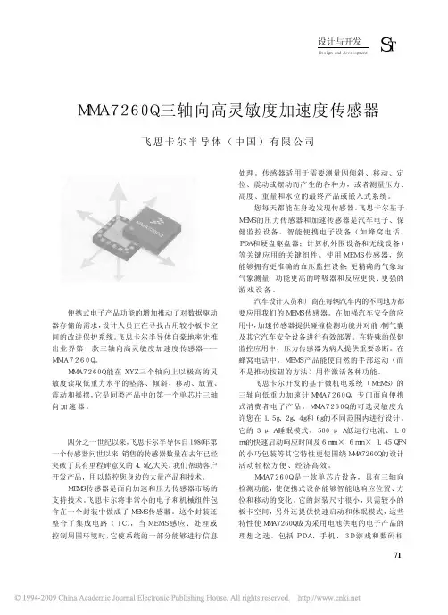


压电式加速度传感器及其应用一、压电式加速度传感器原理压电式加速度传感器又称压电加速度计。
它也属于惯性式传感器。
它是利用某些物质如石英晶体的压电效应,在加速度计受振时,质量块加在压电元件上的力也随之变化。
当被测振动频率远低于加速度计的固有频率时,则力的变化与被测加速度成正比。
加速度传感器是一种惯性传感器,它能感受加速度并转换成可用输出信号,被广泛用于航空航天、武器系统、汽车、消费电子等。
实际电路图如下:二、压电式加速度传感器构成元件预压弹簧压电元件外壳质量块基座常用的压电式加速度计的结构形式如图所示,是由预压弹簧,质量块,基座,压电元件和外壳组成。
图中为环形剪切型,结构简单,能做成极小型、高共振频率的加速度计,环形质量块粘到装在中心支柱上的环形压电元件上。
由于粘结剂会随温度增高而变软,因此最高工作温度受到限制。
三、压电式加速度传感器的实际应用加速度传感器应用范围广泛,一般来讲它有六种检测感应功能:倾斜度检测、运动检测、定位检测、震动检测、振动检测和自由落下检测。
(一)倾斜度检测加速度传感器水平放置时,在重力作用下经激励有一定幅度的输出,当与重力方向有倾角时,传感器信号输出幅度会有所变化,对两种状态下信号输出进行比较计算可推算出倾斜角的大小,应用双轴、三轴加速度传感器就可测出任意倾斜角的大小和方向。
利用加速度传感器测量倾斜度的这种检测感应功能,加速度传感器可应用于倾斜仪、倾斜度侦测电子罗盘、图像旋转、文本滚动浏览/用户界面、LCD投影和物理治疗法等方面。
飞思卡尔半导体公司推出的MMA7260Q三轴加速度传感器是用于倾角测量的典型应用之一,它以重力为输入矢量来决定物体在空间的姿态。
把加速度传感器固定于物体的水平面上,当物体姿态改变时,加速度传感器的敏感轴随之转动一定角度,由于重力的作用,传感器敏感轴上的加速度会发生改变,因此可通过测量加速度的变化来反映物体姿态的变化。
(二) 运动检测在进行运动检测时,需要考虑几个因素:如何计算它的位移,g 值的范围选择及使用量测轴。
飞思卡尔半导推出款包含一个电容式压力传感器-新品速递飞思卡尔半导体近日推出业内款包含一个电容式压力传感器,并面向超低功耗和感应的胎压监控系统(TPMS)。
飞思卡尔MPXY8300系统封装器件提供了高度集成的、经济高效的解决方案,该解决方案集先进的压力传感器和8位微控制器(MCU)、两轴加速仪和无线射频(RF)于一身。
飞思卡尔的MPXY8300系统封装解决方案旨在满足汽车的安全需求,实现的、及时的胎压监控。
合适的胎压有助于减少威胁生命安全的爆胎事件的概率、增强道路通过能力、提高燃油效率、延长轮胎使用寿命、降低车辆保有成本。
据美国国家公路安全管理局(NHTSA)的估计,在美国,每年有23000起交通事故和500多起伤亡事故是由于不适当的充气轮胎(充气不足或过多)而引起的爆胎造成的。
为了控制与轮胎有关的事故,NHTSA规定,2022年前,重量超过10000镑的新车都必须采用TPMS技术。
TPMS也成为欧洲和亚太地区国家对保障司机安全的要求。
“尽管TPMS设计已经进行了几年的时间,但系统的直接成本和客户拥有成本仍然是汽车制造商所考虑的重要因素,”Strategy Analytics汽车电子部副总裁Chris Webber说,“为了在这些方面有所改进,汽车OEM正在寻求高度集成的TPMS解决方案(如飞思卡尔的TPMS解决方案),其卓越的低功率管理可实现更长的电池寿命,更高的集成度并大大降低了系统成本。
”当任何一个轮胎(包括备胎)的胎压未处于水平上时,飞思卡尔的MPXY8300 TPMS解决方案能够及时提醒司机,以帮助他们维持一个适当的胎压。
这个高度集成的MPXY8300系统是一个安装在车轮上的应用,它通过把TPMS的必要数字、模拟和传感器功能结合到一个紧凑的封装内,帮助汽车工程师减少开发周期时间、组件数量和系统成本。
除了是一家的8位汽车MCU供应商外,飞思卡尔还能够为汽车应用提供各种高性能的模拟、电源管理、压力和惯性传感器,以及RF器件。
飞思卡尔基于MEMS的传感器技术
微机电系统(MEMS)是飞思卡尔应用于加速度和压力传感器的技术。
基于MEMS的传感器产品有一个接口,通过该接口可以感应、处理和/或控制周围环境。
飞思卡尔基于MEMS的这一类传感器器件将非常小的机电组件集成在单个芯片上。
基于MEMS的传感器是汽车电子、医疗设备、硬盘驱动器、计算机外设、无线设备及手机、PDA等智能便携式电子设备的重要组件。
MEMS的优点:低成本、低功耗、小型化、高性能、集成
飞思卡尔的领先地位
近30年来,飞思卡尔半导体不断开发各种基于MEMS的传感器。
用于生产传感器的工艺技术大体上分为两类:立体微加工和表面微加工。
我们公司生产加速度传感器和压力传感器。
飞思卡尔是大规模量产基于MEMS传感器的制造商。
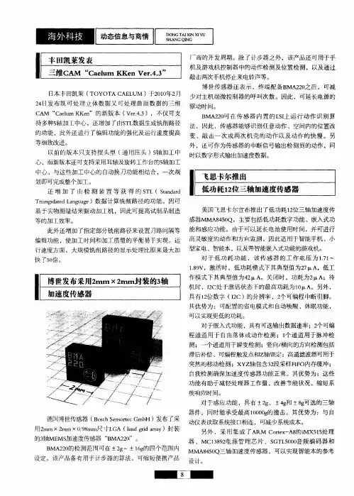
飞思卡尔 MMA7455 三轴数字加速度传感器模块,IIC/SPI接口,全新原装芯片!板子上集成5V转3.3V芯片,用于5V供电的单片机系统更方便!MMA7455数字加速度传感器模块MMA745是一款数字输出(I2C/SPI)、低功耗、紧凑型电容式微机械加速度计,具有信号调理、低通滤波器、温度补偿、自测、可配置通过中断引脚(INT1 或INT2)检测0g、以及脉冲检测(用于快?僭硕 觳猓┑裙δ堋?0g偏置和灵敏度是出厂配置,无需外部器件。
客户可使用指定的0g寄存器和g-Select量程选择对0g偏置进行校准,量程可通过命令选择3个加速度范围(2g/4g/8g)。
MMA745xL系列具备待机模式,使它成为以电池为电源的手持式电子器件的理想选择。
MMA7455数字三轴加速度传感器模块核心为飞思卡尔公司的MMA7455L数字三轴加速度传感器,该模块设计使用官方推荐设计,板卡线路经过高电磁兼容设计和优化,具有输出精确,体积小,工作可靠,各种标识清晰,扩展性好等特点。
MMA7455L芯片安装在带DIP插脚的印刷电路板(PCB)上,它允许客户将其集成到特定的设计应用对产品进行评估。
这样客户就能够在他们自己硬件和软件环境内灵活地评估器件。
模块主要参数· Z 轴自测·低压操作:2.4V – 3.6V·用于偏置校准的用户指·定寄存器·可编程阀值中断输出·电平检测模式运动识别(冲击、震·动、自由下落)·脉冲检测模式单脉冲或双脉冲识别·灵敏度64 LSB/g @ 2g /8g 10位模式· 8位模式的可选灵敏度(±2g、±4g、±8g)·可靠的设计、高抗震·性(5000g)·环保型产品·低成本目标应用·手机/PMP/PDA:图像稳定性, 文字滚动,·移动拨号,·点击静音·硬盘驱动(HDD):自由下落检测·笔记本电脑:自由下落检测,·防盗·计步器·运动传感,·故障记录仪。
Freescale为消费电子应用提供双轴向加速度传感器
佚名
【期刊名称】《电子元器件应用》
【年(卷),期】2004(006)007
【摘要】摩托罗拉旗下全资子公司飞思卡尔半导体 (Freescale Semiconductor)日前宣布为消费电子市场推出了一款加速度传感器。
飞思卡尔创新的 MMA62xxQ 系列MEMS传感器专为终端产品和嵌入式系统而设计,满足它们对倾斜、运动、定位、震动和振动等微小变化的测量需求。
【总页数】1页(P36)
【正文语种】中文
【中图分类】TP212
【相关文献】
1.双轴加速度传感器ADXL210E及在三维鼠标中的应用 [J], 王海红
2.双轴加速度传感器在微小型飞行器姿态测量中的应用研究 [J], 李叶紫;胡辉;刘昕
3.飞思卡尔为消费电子应用提供双轴向传感器--MMA6200Q系列XY-轴高灵敏度加速度传感器 [J],
4.飞思卡尔为消费电子应用提供双轴向传感器 [J],
5.飞思卡尔为消费电子应用提供双轴向传感器——MMA6200Q系列XY-轴高灵敏度加速度传感器 [J],
因版权原因,仅展示原文概要,查看原文内容请购买。
加速度模块规格书
ACCELEROMETER-101加速度模块,测量物体运动或震动的三轴全方向的加速度值,测量范围达到±8g。
加速度模块采集到的物体运动的实际加速度值,直接从串口输出。
,输出的数据格式有三种形式,分别为16进制数据、十进制数据和根据传感器芯片手册中的数据规格转换成的实际加速度值。
另外,本加速度模块可以通过串口设置加速度阀值。
当加速度模块测量到物体运动的加速度达到此阀值时,将通过IO口输出一个高电平或低电平的信号,作为中断信号使用。
加速度值的输出数据假设如下:
X=FB 251 -0.3g
Y=FE 254 -0.1g
Z= 11 017 +1.1g
其中X、Y、Z分别表示三轴,其中X=FB 251 -0.3g中的FB表示测量到的16进制加速度值,251表示从16进制转换成十进制的数据,-0.3g表示根据加速度传感器芯片的数据规格转换成的物体运动的加速度值,-0.3g中的负号表示物体的运动方向为X轴的反方向,-0.3g中的0.3g表示物体以0.3g的加速度值向X轴的反方向做加速运动。
加速度模块的参数:
工作电压: +5V
工作电流: ≤40mA
加速度值参数:
测量方向:三轴全方向
带 宽:62.5Hz 或 125Hz
灵 敏 度:16 LSB/g @ 8g in 8-bit Mode
自检测:支持Z轴自检测加速度
加速度值测量范围: ≤±8g
抗震动的最大忍受度:≤1000g
加速度模块研发生产商:安徽合嵌电子科技公司
QQ: 1094606988
Email: xinxidixcq@。
飞思卡尔推出全新的工业加速度传感器
飞思卡尔半导体(NYSE:FSL)日前推出了一款全新的高带宽三轴模拟加速度传感器,用于检测工业电机及设备的超高频运动和振动。
基于在汽车传感器领域的丰富经验和强大实力,飞思卡尔广泛的传感器产品组合,包括其不断增长、备受欢迎的工业和医疗市场器件,都获得了市场的高度认可。
过去五年,客户每年在超过150个独立的传感应用中采用飞思卡尔传感器。
飞思卡尔全新的FXLN83xxQ加速度传感器突显出公司的工业传感实力。
新器件可以捕获那些精确度有欠缺的传感器往往会丢失的加速度信息(此类传感器通常部署在消费电子产品中,如智能手机和健身活动监测器)。
新推的器件使智能算法能更好地针对预测型维护和环境监控应用执行故障预测。
飞思卡尔副总裁兼传感器解决方案事业部总经理Babak Taheri 表示:传感器的数据信息驱动着效率的提高、并在工业和医疗市场培育出极具吸引力的新商业模式。
飞思卡尔的系统和应用团队与客户紧密合作,将我们众多的传感器产品组合与我们广泛系列的微控制器结合,以满足新应用、迎接新商机。
新的解决方案能帮助系统设计人员收集和利用传感器数据,推动新一代工业和医疗应用的分析和智能。