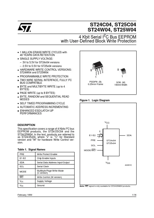
ST24C04, ST25C04 ST24W04, ST25W044 Kbit Serial I 2C Bus EEPROMwith User-Defined Block Write ProtectionFebruary 19991/16AI00851E2E1-E2SDAV CCST24x04ST25x04MODE/WC*SCLV SSPRE Figure 1. Logic Diagram1 MILLION ERASE/WRITE CYCLES with 40 YEARS DATA RETENTION SINGLE SUPPLY VOLTAGE:–3V to 5.5V for ST24x04 versions –2.5V to 5.5V for ST25x04 versionsHARDWARE WRITE CONTROL VERSIONS:ST24W04 and ST25W04PROGRAMMABLE WRITE PROTECTION TWO WIRE SERIAL INTERFACE, FULLY I 2C BUS COMPATIBLEBYTE and MULTIBYTE WRITE (up to 4BYTES)PAGE WRITE (up to 8 BYTES)BYTE, RANDOM and SEQUENTIAL READ MODESSELF TIMED PROGRAMMING CYCLE AUTOMATIC ADDRESS INCREMENTING ENHANCED ESD/LATCH UP PERFORMANCESDESCRIPTIONThis specification covers a range of 4 Kbits I 2C bus EEPROM products, the ST24/25C04 and the ST24/25W04. In the text, products are referred to as ST24/25x04, where "x" is: "C" for Standard version and "W" for hardware Write Control ver-sion.PRE Write Protect Enable E1-E2Chip Enable InputsSDA Serial Data Address Input/Output SCL Serial ClockMODE Multibyte/Page Write Mode (C version)WC Write Control (W version)V CC Supply Voltage V SSGroundTable 1. Signal Names81SO8 (M)150mil Width81PSDIP8 (B)0.25mm FrameNote: WC signal is only available for ST24/25W04 products.The ST24/25x04 are 4 Kbit electrically erasable programmable memories (EEPROM), organized as 2 blocks of 256 x8 bits. They are manufactured in STMicroelectronics’s Hi-Endurance Advanced CMOS technology which guarantees an endur-ance of one million erase/write cycles with a data retention of 40 years.Both Plastic Dual-in-Line and Plastic Small Outline packages are available.The memories are compatible with the I 2C stand-ard, two wire serial interface which uses a bi-direc-tional data bus and serial clock. The memoriescarry a built-in 4 bit, unique device identification code (1010) corresponding to the I 2C bus defini-tion. This is used together with 2 chip enable inputs (E2, E1) so that up to 4 x 4K devices may be attached to the I 2C bus and selected individually.The memories behave as a slave device in the I 2C protocol with all memory operations synchronized by the serial clock. Read and write operations are initiated by a START condition generated by the bus master. The START condition is followed by a stream of 7 bits (identification code 1010), plus one read/write bit and terminated by an acknowledge bit.SDAV SSSCL MODE/WC E1PRE V CCE2AI00852EST24x04ST25x0412348765Figure 2A. DIP Pin Connections 1AI01107E2348765SDAV SSSCL MODE/WC E1PRE V CCE2ST24x04ST25x04Figure 2B. SO Pin ConnectionsDESCRIPTION (cont’d)Symbol ParameterValue Unit T A Ambient Operating Temperature –40 to 125 °C T STG Storage Temperature –65 to 150°C T LEAD Lead Temperature, Soldering (SO8 package)(PSDIP8 package)40 sec 10 sec215260°C V IO Input or Output Voltages –0.6 to 6.5 V V CC Supply Voltage–0.3 to 6.5V V ESDElectrostatic Discharge Voltage (Human Body model) (2)4000V Electrostatic Discharge Voltage (Machine model) (3)500VNotes:1.Except for the rating "Operating Temperature Range", stresses above those listed in the Table "Absolute Maximum Ratings"may cause permanent damage to the device. These are stress ratings only and operation of the device at these or any other conditions above those indicated in the Operating sections of this specification is not implied. Exposure to Absolute MaximumRating conditions for extended periods may affect device reliability. Refer also to the STMicroelectronics SURE Program and other relevant quality documents.-STD-883C, 3015.7 (100pF, 1500 Ω).3.EIAJ IC-121 (Condition C) (200pF, 0 Ω).Table 2. Absolute Maximum Ratings (1)2/16ST24/25C04, ST24/25W04ModeRW bit MODE Bytes Initial SequenceCurrent Address Read ’1’X 1START, Device Select, RW = ’1’Random Address Read ’0’X1START, Device Select, RW = ’0’, Address,’1’reSTART, Device Select, RW = ’1’Sequential Read ’1’X 1 to 512Similar to Current or Random Mode Byte Write ’0’X 1START, Device Select, RW = ’0’Multibyte Write (2)’0’V IH 4START, Device Select, RW = ’0’Page Write’0’V IL8START, Device Select, RW = ’0’Notes:1.X = V IH or V IL2.Multibyte Write not available in ST24/25W04 versions.Table 4. Operating Modes (1)Device CodeChip EnableBlock Select RW Bitb7b6b5b4b3b2b1b0Device Select11E2E1A8RWNote: The MSB b7 is sent first.Table 3. Device Select CodeWhen writing data to the memory it responds to the 8 bits received by asserting an acknowledge bit during the 9th bit time. When data is read by the bus master, it acknowledges the receipt of the data bytes in the same way. Data transfers are termi-nated with a STOP condition.Power On Reset: V CC lock out write protect. In order to prevent data corruption and inadvertent write operations during power up, a Power On Reset (POR) circuit is implemented. Until the V CC voltage has reached the POR threshold value, the internal reset is active, all operations are disabled and the device will not respond to any command.In the same way, when V CC drops down from the operating voltage to below the POR threshold value, all operations are disabled and the device will not respond to any command. A stable V CC must be applied before applying any logic signal.SIGNAL DESCRIPTIONSSerial Clock (SCL). The SCL input pin is used to synchronize all data in and out of the memory. A resistor can be connected from the SCL line to V CC to act as a pull up (see Figure 3).Serial Data (SDA). The SDA pin is bi-directional and is used to transfer data in or out of the memory.It is an open drain output that may be wire-OR’edwith other open drain or open collector signals on the bus. A resistor must be connected from the SDA bus line to V CC to act as pull up (see Figure 3).Chip Enable (E1 - E2). These chip enable inputs are used to set the 2 least significant bits (b2, b3)of the 7 bit device select code. These inputs may be driven dynamically or tied to V CC or V SS to establish the device select code.Protect Enable (PRE). The PRE input pin, in ad-dition to the status of the Block Address Pointer bit (b2, location 1FFh as in Figure 7), sets the PRE write protection active.Mode (MODE). The MODE input is available on pin 7 (see also WC feature) and may be driven dynami-cally. It must be at V IL or V IH for the Byte Write mode, V IH for Multibyte Write mode or V IL for Page Write mode. When unconnected, the MODE input is internally read as V IH (Multibyte Write mode). Write Control (WC). An hardware Write Control feature (WC) is offered only for ST24W04 and ST25W04 versions on pin 7. This feature is usefull to protect the contents of the memory from any erroneous erase/write cycle. The Write Control sig-nal is used to enable (WC = V IH ) or disable (WC =V IL ) the internal write protection. When uncon-nected, the WC input is internally read as V IL and the memory area is not write protected.3/16ST24/25C04, ST24/25W04AI01100V CCC BUSSDA R LMASTERR LSCLC BUS10020030040048121620C BUS (pF)R L m a x (k Ω)V CC = 5VFigure 3. Maximum R L Value versus Bus Capacitance (C BUS ) for an I 2C BusThe devices with this Write Control feature no longer support the Multibyte Write mode of opera-tion, however all other write modes are fully sup-ported.Refer to the AN404 Application Note for more de-tailed information about Write Control feature.DEVICE OPERATION I 2C Bus BackgroundThe ST24/25x04 support the I 2C protocol. This protocol defines any device that sends data onto the bus as a transmitter and any device that reads the data as a receiver. The device that controls the data transfer is known as the master and the other as the slave. The master will always initiate a data transfer and will provide the serial clock for syn-chronisation. The ST24/25x04 are always slave devices in all communications.Start Condition. START is identified by a high to low transition of the SDA line while the clock SCL is stable in the high state. A START condition must precede any command for data transfer. Except during a programming cycle, the ST24/25x04 con-tinuously monitor the SDA and SCL signals for a START condition and will not respond unless one is given.Stop Condition. STOP is identified by a low to high transition of the SDA line while the clock SCL is stable in the high state. A STOP condition termi-nates communication between the ST24/25x04and the bus master. A STOP condition at the end of a Read command, after and only after a No Acknowledge, forces the standby state. A STOP condition at the end of a Write command triggers the internal EEPROM write cycle.Acknowledge Bit (ACK). An acknowledge signal is used to indicate a successfull data transfer. The bus transmitter, either master or slave, will release the SDA bus after sending 8 bits of data. During the 9th clock pulse period the receiver pulls the SDA bus low to acknowledge the receipt of the 8 bits of data.Data Input. During data input the ST24/25x04sample the SDA bus signal on the rising edge of the clock SCL. Note that for correct device opera-tion the SDA signal must be stable during the clock low to high transition and the data must change ONLY when the SCL line is low.Memory Addressing. To start communication be-tween the bus master and the slave ST24/25x04,the master must initiate a START condition. Follow-ing this, the master sends onto the SDA bus line 8bits (MSB first) corresponding to the device select code (7 bits) and a READ or WRITE bit.SIGNAL DESCRIPTIONS (cont’d)4/16ST24/25C04, ST24/25W04Symbol ParameterTest ConditionMinMax Unit C IN Input Capacitance (SDA)8pF C IN Input Capacitance (other pins)6pF Z WCL WC Input Impedance (ST24/25W04)V IN ≤ 0.3 V CC 520k ΩZ WCH WC Input Impedance (ST24/25W04)V IN ≥ 0.7 V CC500k Ωt LPLow-pass filter input time constant (SDA and SCL)100nsNote: 1. Sampled only, not 100% tested.Table 5. Input Parameters (1) (T A = 25 °C, f = 100 kHz )Symbol ParameterTest Condition MinMax Unit I LI Input Leakage Current 0V ≤ V IN ≤ V CC ±2µA I LO Output Leakage Current 0V ≤ V OUT ≤ V CC SDA in Hi-Z ±2µA I CCSupply Current (ST24 series)V CC = 5V, f C = 100kHz (Rise/Fall time < 10ns)2mA Supply Current (ST25 series)V CC = 2.5V, f C = 100kHz 1mA I CC1Supply Current (Standby)(ST24 series)V IN = V SS or V CC ,V CC = 5V 100µA V IN = V SS or V CC , V CC = 5V, f C = 100kHz 300µA I CC2Supply Current (Standby) (ST25 series)V IN = V SS or V CC , V CC = 2.5V 5µA V IN = V SS or V CC , V CC = 2.5V, f C = 100kHz50µA V IL Input Low Voltage (SCL, SDA)–0.30.3 V CC V V IH Input High Voltage (SCL, SDA)0.7 V CC V CC + 1V V IL Input Low Voltage(E1-E2, PRE, MODE, WC)–0.30.5V V IH Input High Voltage(E1-E2, PRE, MODE, WC)V CC – 0.5V CC + 1V V OLOutput Low Voltage (ST24 series)I OL = 3mA, V CC = 5V 0.4V Output Low Voltage (ST25 series)I OL = 2.1mA, V CC = 2.5V0.4VTable 6. DC Characteristics(T A = 0 to 70°C, –20 to 85°C or –40 to 85°C; V CC = 3V to 5.5V or 2.5V to 5.5V)5/16ST24/25C04, ST24/25W04The 4 most significant bits of the device select codeare the device type identifier, corresponding to the I 2C bus definition. For these memories the 4 bits are fixed as 1010b. The following 2 bits identify the specific memory on the bus. They are matched to the chip enable signals E2, E1. Thus up to 4 x 4K memories can be connected on the same bus giving a memory capacity total of 16 Kbits. After a START condition any memory on the bus will iden-tify the device code and compare the following 2bits to its chip enable inputs E2, E1.The 7th bit sent is the block number (one block =256 bytes). The 8th bit sent is the read or write bit (RW), this bit is set to ’1’ for read and ’0’ for write operations. If a match is found, the corresponding memory will acknowledge the identification on the SDA bus during the 9th bit time.Input Rise and Fall Times ≤ 50nsInput Pulse Voltages0.2V CC to 0.8V CCInput and Output Timing Ref. Voltages 0.3V CC to 0.7V CCAC MEASUREMENT CONDITIONSAI008250.8V CC0.2V CC0.7V CC 0.3V CCFigure 4. AC Testing Input Output WaveformsDEVICE OPERATION (cont’d)Symbol Alt ParameterMinMax Unit t CH1CH2t R Clock Rise Time 1µs t CL1CL2t F Clock Fall Time 300ns t DH1DH2t R Input Rise Time 1µs t DL1DL1t F Input Fall Time300ns t CHDX (1)t SU:STA Clock High to Input Transition 4.7µs t CHCL t HIGH Clock Pulse Width High4µs t DLCL t HD:STA Input Low to Clock Low (START)4µs t CLDX t HD:DAT Clock Low to Input Transition 0µs t CLCH t LOW Clock Pulse Width Low4.7µs t DXCX t SU:DAT Input Transition to Clock Transition 250ns t CHDH t SU:STO Clock High to Input High (STOP) 4.7µs t DHDL t BUF Input High to Input Low (Bus Free) 4.7µs t CLQV (2)t AA Clock Low to Next Data Out Valid 0.3 3.5µs t CLQX t DH Data Out Hold Time 300ns f C f SCL Clock Frequency 100kHz t W (3)t WRWrite Time10msNotes:1.For a reSTART condition, or following a write cycle.2.The minimum value delays the falling/rising edge of SDA away from SCL = 1 in order to avoid unwanted START and/or STOP conditions.3.In the Multibyte Write mode only, if accessed bytes are on two consecutive 8 bytes rows (6 address MSB are not constant) themaximum programming time is doubled to 20ms.Table 7. AC Characteristics(T A = 0 to 70°C, –20 to 85°C or –40 to 85°C; V CC = 3V to 5.5V or 2.5V to 5.5V)6/16ST24/25C04, ST24/25W04SCL SDA INSCL SDA OUTSCL SDA INtCHCLtDLCLtCHDXSTARTCONDITIONtCLCHtDXCXtCLDXSDAINPUTSDACHANGEtCHDHtDHDLSTOP &BUS FREEDATA VALIDtCLQV tCLQXDATA OUTPUTtCHDHSTOPCONDITIONtCHDXSTARTCONDITIONWRITE CYCLEtWAI00795BFigure 5. AC WaveformsWrite OperationsThe Multibyte Write mode (only available on the ST24/25C04 versions) is selected when the MODE pin is at V IH and the Page Write mode when MODE pin is at V IL. The MODE pin may be driven dynami-cally with CMOS input levels.Following a START condition the master sends a device select code with the RW bit reset to ’0’. The memory acknowledges this and waits for a byte address. The byte address of 8 bits provides ac-cess to one block of 256 bytes of the memory. After receipt of the byte address the device again re-sponds with an acknowledge.For the ST24/25W04 versions, any write command with WC = 1 will not modify the memory content. Byte Write. In the Byte Write mode the master sends one data byte, which is acknowledged by the memory. The master then terminates the transfer by generating a STOP condition. The Write mode is independant of the state of the MODE pin which could be left floating if only this mode was to be used. However it is not a recommended operating mode, as this pin has to be connected to either V IH or V IL, to minimize the stand-by current.7/16ST24/25C04, ST24/25W04SCL SDASCL SDASDASTARTCONDITIONSDAINPUTSDACHANGEAI00792STOPCONDITION 123789MSB ACKSTARTCONDITIONSCL123789MSB ACKSTOPCONDITION Figure 6. I2C Bus ProtocolMultibyte Write. For the Multibyte Write mode, the MODE pin must be at V IH. The Multibyte Write mode can be started from any address in the memory. The master sends from one up to 4 bytes of data, which are each acknowledged by the mem-ory. The transfer is terminated by the master gen-erating a STOP condition. The duration of the write cycle is t W = 10ms maximum except when bytes are accessed on 2 rows (that is have different values for the 6 most significant address bits A7-A2), the programming time is then doubled to a maximum of 20ms. Writing more than 4 bytes in the Multibyte Write mode may modify data bytes in an adjacent row (one row is 8 bytes long). However, the Multibyte Write can properly write up to 8 consecutive bytes as soon as the first address of these 8 bytes is the first address of the row, the 7 following bytes being written in the 7 following bytes of this same row.Page Write. For the Page Write mode, the MODE pin must be at V IL. The Page Write mode allows up to 8 bytes to be written in a single write cycle, provided that they are all located in the same ’row’in the memory: that is the 5 most significant mem-8/16ST24/25C04, ST24/25W04ory address bits (A7-A3) are the same inside one block. The master sends from one up to 8 bytes of data, which are each acknowledged by the mem-ory. After each byte is transfered, the internal byte address counter (3 least significant bits only) is incremented. The transfer is terminated by the master generating a STOP condition. Care must be taken to avoid address counter ’roll-over’ which could result in data being overwritten. Note that, for any write mode, the generation by the master of the STOP condition starts the internal memory pro-gram cycle. All inputs are disabled until the comple-tion of this cycle and the memory will not respond to any request.Minimizing System Delays by Polling On ACK.During the internal write cycle, the memory discon-nects itself from the bus in order to copy the data from the internal latches to the memory cells. The maximum value of the write time (t W ) is given in the AC Characteristics table, since the typical time is shorter, the time seen by the system may be re-duced by an ACK polling sequence issued by the master.WRITE Cycle in ProgressAI01099BNext Operation is Addressing the MemorySTART Condition DEVICE SELECT with RW = 0ACK ReturnedYESNOYESNOReSTARTSTOPProceedWRITE OperationProceedRandom Address READ OperationSend Byte AddressFirst byte of instruction with RW = 0 already decoded by ST24xxxFigure 8. Write Cycle Polling using ACKAI00855B1FFhb7b3b2XX100hBlock 1Block 0Protect Flag Enable = 0Disable = 18 byte boundary address Protect Location Figure 7. Memory Protection9/16ST24/25C04, ST24/25W04The sequence is as follows:–Initial condition: a Write is in progress (see Figure 8).–Step 1: the Master issues a START condition followed by a Device Select byte (1st byte of the new instruction).–Step 2: if the memory is busy with the internal write cycle, no ACK will be returned and the master goes back to Step 1. If the memory has terminated the internal write cycle, it will re-spond with an ACK, indicating that the memory is ready to receive the second part of the next instruction (the first byte of this instruction was already sent during Step 1).Write Protection. Data in the upper block of 256bytes of the memory may be write protected. The memory is write protected between a boundary address and the top of memory (address 1FFh)when the PRE input pin is taken high and when the Protect Flag (bit b2 in location 1FFh) is set to ’0’.The boundary address is user defined by writing it in the Block Address Pointer. The Block Address Pointer is an 8 bit EEPROM register located at the address 1FFh. It is composed by 5 MSBs Address Pointer, which defines the bottom boundary ad-dress, and 3 LSBs which must be programmed atDEVICE OPERATION (cont’d)’0’. This Address Pointer can therefore address a boundary in steps of 8 bytes.The sequence to use the Write Protected feature is:–write the data to be protected into the top of the memory, up to, but not including, location 1FFh;–set the protection by writing the correct bottom boundary address in the Address Pointer (5MSBs of location 1FFh) with bit b2 (Protect flag)set to ’0’. Note that for a correct fonctionality of the memory, all the 3 LSBs of the Block Address Pointer must also be programmed at ’0’.The area will now be protected when the PRE input pin is taken High. While the PRE input pin is read at ’0’ by the memory, the location 1FFh can be used as a normal EEPROM byte.Caution: Special attention must be used when using the protect mode together with the Multibyte Write mode (MODE input pin High). If the Multibyte Write starts at the location right below the first byte of the Write Protected area, then the instruction will write over the first 3 bytes of the Write Protected area. The area protected is therefore smaller than the content defined in the location 1FFh, by 3 bytes.This does not apply to the Page Write mode as the address counter ’roll-over’ and thus cannot go above the 8 bytes lower boundary of the protected area.S T O PS T A R TBYTE WRITEDEV SELBYTE ADDR DATA INS T A R TMULTIBYTE ANDPAGE WRITEDEV SEL BYTE ADDR DATA IN 1DATA IN 2AI00793S T O PDATA IN NACKACKACKR/W ACKACKACKR/WACKACKFigure 9. Write Modes Sequence (ST24/25C04)10/16ST24/25C04, ST24/25W04S T O PS T A R TBYTE WRITEDEV SELBYTE ADDR DATA INWCS T A R TPAGE WRITEDEV SELBYTE ADDR DATA IN 1WCDATA IN 2AI01101BPAGE WRITE (cont'd)WC (cont'd)S T O PDATA IN NACKACKACKR/WACKACKACKR/WACKACKFigure 10. Write Modes Sequence with Write Control = 1 (ST24/25W04)Read OperationsRead operations are independent of the state of the MODE pin. On delivery, the memory content is set at all "1’s" (or FFh).Current Address Read. The memory has an inter-nal byte address counter. Each time a byte is read,this counter is incremented. For the Current Ad-dress Read mode, following a START condition,the master sends a memory address with the RW bit set to ’1’. The memory acknowledges this and outputs the byte addressed by the internal byte address counter. This counter is then incremented.The master does NOT acknowledge the byte out-put, but terminates the transfer with a STOP con-dition.Random Address Read. A dummy write is per-formed to load the address into the address counter, see Figure 11. This is followed by another START condition from the master and the byte address is repeated with the RW bit set to ’1’. The memory acknowledges this and outputs the byte addressed. The master have to NOT acknowledge the byte output, but terminates the transfer with a STOP condition.Sequential Read. This mode can be initiated with either a Current Address Read or a Random Ad-dress Read. However, in this case the master DOES acknowledge the data byte output and the memory continues to output the next byte in se-quence. To terminate the stream of bytes, the master must NOT acknowledge the last byte out-11/16put, but MUST generate a STOP condition. The output data is from consecutive byte addresses,with the internal byte address counter automat-ically incremented after each byte output. After a count of the last memory address, the addresscounter will ’roll- over’ and the memory will continue to output data.Acknowledge in Read Mode. In all read modes the ST24/25x04 wait for an acknowledge during the 9th bit time. If the master does not pull the SDA line low during this time, the ST24/25x04 terminate the data transfer and switches to a standby state.S T A R TDEV SEL *BYTE ADDRS T A R TDEV SELDATA OUT 1AI00794CDATA OUT NS T O PS T A R TCURRENT ADDRESS READDEV SELDATA OUTRANDOM ADDRESS READS T O PS T A R TDEV SEL *DATA OUTSEQUENTIAL CURRENT READS T O P DATA OUT NS T A R TDEV SEL *BYTE ADDR SEQUENTIAL RANDOM READS T A R TDEV SEL *DATA OUT 1S T O PACKR/WNO ACKACKR/WACKACK R/WACKACK ACK NO ACKR/WNO ACKACKACKR/WACK ACKR/WACK NO ACKFigure 11. Read Modes SequenceNote:*The 7 Most Significant bits of DEV SEL bytes of a Random Read (1st byte and 3rd byte) must be identical.DEVICE OPERATION (cont’d)12/16ORDERING INFORMATION SCHEMENotes: 3 * Temperature range on special request only.Parts are shipped with the memory content set at all "1’s" (FFh).For a list of available options (Operating Voltage, Range, Package, etc...) or for further information on any aspect of this device, please contact the STMicroelectronics Sales Office nearest to you.Operating Voltage ST24C04 3V to 5.5V ST24W04 3V to 5.5V ST25C04 2.5V to 5.5V ST25W04 2.5V to 5.5VRangeStandardHardware Write Control StandardHardware Write ControlPackage B PSDIP80.25mm Frame MSO8 150mil WidthTemperature Range 10 to 70 °C 5–20 to 85 °C 6–40 to 85 °C 3 *–40 to 125 °COption TRTape & Reel PackingExample: ST24C04 M 1 TR13/16PSDIP-aA2A1A Le1DE1EN1CeA eBB1BSymbmm inches TypMin Max TypMin Max A 3.90 5.900.1540.232A10.49–0.019–A2 3.30 5.300.1300.209B 0.360.560.0140.022B1 1.15 1.650.0450.065C 0.200.360.0080.014D 9.209.900.3620.390E 7.62––0.300––E1 6.00 6.700.2360.264e1 2.54––0.100––eA 7.80–0.307–eB –10.00–0.394L 3.00 3.800.1180.150N88Drawing is not to scalePSDIP8 - 8 pin Plastic Skinny DIP , 0.25mm lead frame14/16SO-aENCPBe ADCLA1α1Hh x 45˚Symbmm inches TypMin Max TypMin Max A 1.35 1.750.0530.069A10.100.250.0040.010B 0.330.510.0130.020C 0.190.250.0070.010D 4.80 5.000.1890.197E 3.80 4.000.1500.157e 1.27––0.050––H 5.80 6.200.2280.244h 0.250.500.0100.020L 0.400.900.0160.035α0°8°0°8°N 88CP0.100.004Drawing is not to scaleSO8 - 8 lead Plastic Small Outline, 150 mils body width15/16Information furnished is believed to be accurate and reliable. However, STMicroelectronics assumes no responsibility for the consequences of use of such information nor for any infringement of patents or other rights of third parties which may result from its use. No license is granted by implication or otherwise under any patent or patent rights of STMicroelectronics. Specifications mentioned in this publication are subject to change without notice. This publication supersedes and replaces all information previously supplied. STMicroelectronics products are not authorized for use as critical components in life support devices or systems without express written approval of STMicroelectronics.The ST logo is a registered trademark of STMicroelectronics© 1999 STMicroelectronics - All Rights ReservedSTMicroelectronics GROUP OF COMPANIESAustralia - Brazil - Canada - China - France - Germany - Italy - Japan - Korea - Malaysia - Malta - Mexico - Morocco - The Netherlands - Singapore - Spain - Sweden - Switzerland - Taiwan - Thailand - United Kingdom - U.S.A.16/16。