嵌入式税控POS系统中AT91RM9200有重要作用
- 格式:doc
- 大小:18.00 KB
- 文档页数:4

嵌入式POS机及税控收款机
简介
随着国内零售业及百货业的兴起,收款机即POS(Point Of Sale)已经成为目前最成功并持续发展的嵌入式行业应用。
目前的POS 机具备开放系统,可应用于多种平台和应用软件,也可连接多种外设,还可使用IC 卡、银行卡授权终端,可单机或联网,还可以连接Internet。
采用POS 收银系统,大大降低了收银人员的工作强度,提高收银效率,也为消费者提供了更多的快捷和便利。
嵌入式POS 机可以很好的满足防尘、防震、耐高温、防水的功能。
这些都是一般的PC 机所无法替代的。
华恒科技推出的基于嵌入式ARM9 系列
AT91RM9200 开发的POS 机解决方案具有更高的稳定性、更低的成本、功耗,在市场上的竞争力更加强劲,更受欢迎。
实物图片
特点
-稳定性:采用最主流的ARM9 处理器AT91RM9200@200MHz ,高性能、低功耗,内置资源丰富,外围电路设计简单,保证了生产的方便和稳定性。
包
括处理器在内全部采用QFP 封装的器件,不使用BGA 封装的处理器及其它芯片,适应了国内客户的生产调测水平,并降低PCB 板层数,降低了成本。
-可扩展性:通过内置的两个USB HOST 接口来为产品后续的升级提供高度的扩展性,例如USB 无线网卡、USB 键盘鼠标等输入设备。
-通用性:支持多种LCD 屏及VGA 显示器,包括黑白屏和TFT 真彩屏,分
辨率可支持高达640 乘以480 以上。
并支持触摸屏(800 乘以600)。
满足多种POS 机应用需求。

嵌入式微处理器选型的考虑因素要选好一款处理器,要考虑的因素很多,不单单是纯粹的硬件接口,还需要考虑相关的操作系统、配套的、仿真器,以及工程师的经验和软件支持情况等。
微处理器选型是否得当,将决定项目成败。
当然,并不是说选好微处理器, 就意味着成功,因为项目的成败取决于许多因素;但可以肯定的一点是,微处理器选型不当,将会给项目带来无限的烦恼,甚至导致项目的流产。
1嵌入式微处理器选型的考虑因素在产品开发中,作为核心芯片的微处理器,其自身的功能、性能、可靠性被寄予厚望,因为它的资源越丰富、自带功能越强大,产品开发周期就越短,项目成功率就越高。
但是,任何一款微处理器都不可能尽善尽美,满足每个用户的需要,所以这就涉及选型的问题。
(1)应用领域一个产品的功能、性能一旦定制下来,其所在的应用领域也随之确定。
应用领域的确定将缩小选型的范围,例如:领域产品的工作条件通常比较苛刻,因此对芯片的工作温度通常是宽温的,这样就得选择工业级的芯片,民用级的就被排除在外。
目前,比较常见的应用领域分类有航天航空、通信、计算机、工业控制、医疗系统、、等。
(2)自带资源经常会看到或听到这样的问题:主频是多少?有无内置的以太网MAC?有多少个I/O 口?自带哪些接口?支持在线仿真吗?是否支持OS,能支持哪些OS?是否有外部存储接口?……以上都涉及芯片资源的问题,微处理器自带什么样的资源是选型的一个重要考虑因素。
芯片自带资源越接近产品的需求,产品开发相对就越简单。
(3)可扩展资源硬件平台要支持OS、RAM和ROM,对资源的要求就比较高。
芯片一般都有内置RAM和ROM,但其容量一般都很小,内置512 KB就算很大了,但是运行OS 一般都是兆级以上。
这就要求芯片可扩展存储器。
⑷功耗单看“功耗”是一个较为抽象的名词。
这里举几个形象的例子:①夏天使用空调时,家里的电费会猛增。
这是因为空调是高功耗的家用电器,这时人们会想,“要是空调能像日光灯那样省电就好了”。


Features Array•Incorporates the ARM920T™ ARM® Thumb® Processor–200 MIPS at 180 MHz, Memory Management Unit–16-KByte Data Cache, 16-KByte Instruction Cache, Write Buffer–In-circuit Emulator including Debug Communication Channel–Mid-level Implementation Embedded Trace Macrocell (256-ball BGA Package Only)•Low Power: On VDDCORE 24.4 mA in Normal Mode, 520 µA in Standby Mode •Additional Embedded Memories–16K Bytes of SRAM and 128K Bytes of ROM•External Bus Interface (EBI)–Supports SDRAM, Static Memory, Burst Flash, Glueless Connection toCompactFlash® and NAND Flash/SmartMedia™•System Peripherals for Enhanced Performance:–Enhanced Clock Generator and Power Management Controller–Two On-chip Oscillators with Two PLLs–Very Slow Clock Operating Mode and Software Power Optimization Capabilities –Four Programmable External Clock Signals–System Timer Including Periodic Interrupt, Watchdog and Second Counter–Real-time Clock with Alarm Interrupt–Debug Unit, Two-wire UART and Support for Debug Communication Channel–Advanced Interrupt Controller with 8-level Priority, Individually Maskable Vectored Interrupt Sources, Spurious Interrupt Protected–Seven External Interrupt Sources and One Fast Interrupt Source–Four 32-bit PIO Controllers with Up to 122 Programmable I/O Lines, Input Change Interrupt and Open-drain Capability on Each Line–20-channel Peripheral DMA Controller (PDC)•Ethernet MAC 10/100 Base-T–Media Independent Interface (MII) or Reduced Media Independent Interface (RMII)–Integrated 28-byte FIFOs and Dedicated DMA Channels for Receive and Transmit •USB 2.0 Full Speed (12 Mbits per second) Host Double Port–Dual On-chip Transceivers (Single Port Only on 208-lead PQFP Package)–Integrated FIFOs and Dedicated DMA Channels•USB 2.0 Full Speed (12 Mbits per second) Device Port–On-chip Transceiver, 2-Kbyte Configurable Integrated FIFOs•Multimedia Card Interface (MCI)–Automatic Protocol Control and Fast Automatic Data Transfers–MMC and SD Memory Card-compliant, Supports Up to Two SD Memory Cards •Three Synchronous Serial Controllers (SSC)–Independent Clock and Frame Sync Signals for Each Receiver and Transmitter –I2S Analog Interface Support, Time Division Multiplex Support–High-speed Continuous Data Stream Capabilities with 32-bit Data Transfer •Four Universal Synchronous/Asynchronous Receiver/Transmitters (USART)–Support for ISO7816 T0/T1 Smart Card–Hardware Handshaking–RS485 Support, IrDA Up To 115 Kbps–Full Modem Control Lines on USART1•Master/Slave Serial Peripheral Interface (SPI)–8- to 16-bit Programmable Data Length, 4 External Peripheral Chip Selects•Two 3-channel, 16-bit Timer/Counters (TC)–Three External Clock Inputs, Two Multi-purpose I/O Pins per Channel–Double PWM Generation, Capture/Waveform Mode, Up/Down Capability•Two-wire Interface (TWI)–Master Mode Support, All 2-wire Atmel EEPROMs Supported•IEEE 1149.1 JTAG Boundary Scan on All Digital Pins•Power Supplies–1.65V to 1.95V for VDDCORE, VDDOSC and VDDPLL–3.0V to 3.6V for VDDIOP (Peripheral I/Os) and for VDDIOM (Memory I/Os)Available•in a 208-lead PQFP or 256-ball BGA Package21768IS–ATARM–30-Sep-05AT91RM9200 Summary1.DescriptionThe AT91RM9200 is a complete system-on-chip built around the ARM920T ARM Thumb pro-cessor. It incorporates a rich set of system and application peripherals and standard interfaces in order to provide a single-chip solution for a wide range of compute-intensive applications that require maximum functionality at minimum power consumption at lowest cost.The AT91RM9200 incorporates a high-speed on-chip SRAM workspace, and a low-latency External Bus Interface (EBI) for seamless connection to whatever configuration of off-chip mem-ories and memory-mapped peripherals is required by the application. The EBI incorporates controllers for synchronous DRAM (SDRAM), Burst Flash and Static memories and features specific circuitry facilitating the interface for NAND Flash/SmartMedia and Compact Flash.The Advanced Interrupt Controller (AIC) enhances the interrupt handling performance of the ARM920T processor by providing multiple vectored, prioritized interrupt sources and reducing the time taken to transfer to an interrupt handler.The Peripheral DMA Controller (PDC) provides DMA channels for all the serial peripherals, enabling them to transfer data to or from on- and off-chip memories without processor interven-tion. This reduces the processor overhead when dealing with transfers of continuous data streams.The AT91RM9200 benefits from a new generation of PDC which includes dual pointers that simplify significantly buffer chaining.The set of Parallel I/O (PIO) controllers multiplex the peripheral input/output lines with general-purpose data I/Os for maximum flexibility in device configuration. An input change interrupt, open drain capability and programmable pull-up resistor is included on each line.The Power Management Controller (PMC) keeps system power consumption to a minimum by selectively enabling/disabling the processor and various peripherals under software control. It uses an enhanced clock generator to provide a selection of clock signals including a slow clock (32 kHz) to optimize power consumption and performance at all times.The AT91RM9200 integrates a wide range of standard interfaces including USB 2.0 Full Speed Host and Device and Ethernet 10/100 Base-T Media Access Controller (MAC), which provides connection to a extensive range of external peripheral devices and a widely used networking layer. In addition, it provides an extensive set of peripherals that operate in accordance with sev-eral industry standards, such as those used in audio, telecom, Flash Card, infrared and Smart Card applications.To complete the offer, the AT91RM9200 benefits from the integration of a wide range of debug features including JTAG-ICE, a dedicated UART debug channel (DBGU) and an embedded real time trace. This enables the development and debug of all applications, especially those with real-time constraints.31768IS–ATARM–30-Sep-05 AT91RM9200 Summary2.Block DiagramBold arrows () indicate master-to-slave dependency.Figure 2-1.AT91RM9200 Block Diagram41768IS–ATARM–30-Sep-05AT91RM9200 Summary3.Key FeaturesThis section presents the key features of each block.3.1ARM920T Processor•ARM9TDMI ™-based on ARM ® Architecture v4T•Two instruction sets–ARM ® High-performance 32-bit Instruction Set–Thumb ® High Code Density 16-bit Instruction Set•5-Stage Pipeline Architecture:–Instruction Fetch (F)–Instruction Decode (D)–Execute (E)–Data Memory (M)–Register Write (W)•16-Kbyte Data Cache, 16-Kbyte Instruction Cache–Virtually-addressed 64-way Associative Cache–8 words per line–Write-though and write-back operation–Pseudo-random or Round-robin replacement–Low-power CAM RAM implementation•Write Buffer–16-word Data Buffer–4-address Address Buffer–Software Control Drain•Standard ARMv4 Memory Management Unit (MMU)–Access permission for sections–Access permission for large pages and small pages can be specified separately for each quarter of the pages–16 embedded domains–64 Entry Instruction TLB and 64 Entry Data TLB•8-, 16-, 32-bit Data Bus for Instructions and Data3.2Debug and Test•Integrated Embedded In-Circuit-Emulator•Debug Unit–Two-pin UART–Debug Communication Channel–Chip ID Register•Embedded Trace Macrocell: ETM9 Rev2a–Medium Level Implementation–Half-rate Clock Mode51768IS–ATARM–30-Sep-05 AT91RM9200 Summary–Four Pairs of Address Comparators–Two Data Comparators–Eight Memory Map Decoder Inputs–Two Counters–One Sequencer–One 18-byte FIFO•IEEE1149.1 JT AG Boundary Scan on all Digital Pins3.3Boot Program•Default Boot Program stored in ROM-based products•Downloads and runs an application from external storage media into internal SRAM •Downloaded code size depends on embedded SRAM size•Automatic detection of valid application•Bootloader supporting a wide range of non-volatile memories–SPI DataFlash ® connected on SPI NPCS0–Two-wire EEPROM–8-bit parallel memories on NCS0•Boot Uploader in case no valid program is detected in external NVM and supporting several communication media•Serial communication on a DBGU (XModem protocol)•USB Device Port (DFU Protocol)3.4Embedded Software Services•Compliant with ATPCS•Compliant with AINSI/ISO Standard C •Compiled in ARM/Thumb Interworking•ROM Entry Service•Tempo, Xmodem and DataFlash services•CRC and Sine tables3.5Reset Controller•Two reset input lines (NRST and NTRST) providing, respectively:•Initialization of the User Interface registers (defined in the user interface of each peripheral) and:–Sample the signals needed at bootup–Compel the processor to fetch the next instruction at address zero.•Initialization of the embedded ICE TAP controller.3.6Memory Controller•Programmable Bus Arbiter handling four Masters–Internal Bus is shared by ARM920T, PDC, USB Host Port and Ethernet MACMasters61768IS–ATARM–30-Sep-05AT91RM9200 Summary–Each Master can be assigned a priority between 0 and 7•Address Decoder provides selection for–Eight external 256-Mbyte memory areas–Four internal 1-Mbyte memory areas–One 256-Mbyte embedded peripheral area•Boot Mode Select Option–Non-volatile Boot Memory can be internal or external–Selection is made by BMS pin sampled at reset•Abort Status Registers–Source, Type and all parameters of the access leading to an abort are saved •Misalignment Detector–Alignment checking of all data accesses–Abort generation in case of misalignment•Remap command–Provides remapping of an internal SRAM in place of the boot NVM3.7External Bus Interface•Integrates three External Memory Controllers:–Static Memory Controller–SDRAM Controller–Burst Flash Controller•Additional logic for NAND Flash/SmartMedia and CompactFlash support•Optimized External Bus:–16- or 32-bit Data Bus–Up to 26-bit Address Bus, up to 64-Mbytes addressable–Up to 8 Chip Selects, each reserved to one of the eight Memory Areas–Optimized pin multiplexing to reduce latencies on External Memories•Configurable Chip Select Assignment:–Burst Flash Controller or Static Memory Controller on NCS0–SDRAM Controller or Static Memory Controller on NCS1–Static Memory Controller on NCS3, Optional NAND Flash/SmartMedia Support –Static Memory Controller on NCS4 - NCS6, Optional CompactFlash Support –Static Memory Controller on NCS73.8Static Memory Controller•External memory mapping, 512-Mbyte address space•Up to 8 Chip Select Lines•8- or 16-bit Data Bus•Remap of Boot Memory•Multiple Access Modes supported–Byte Write or Byte Select Lines71768IS–ATARM–30-Sep-05 AT91RM9200 Summary–Two different Read Protocols for each Memory Bank•Multiple device adaptability–Compliant with LCD Module–Programmable Setup Time Read/Write–Programmable Hold Time Read/Write•Multiple Wait State Management–Programmable Wait State Generation–External Wait Request–Programmable Data Float Time3.9SDRAM Controller•Numerous configurations supported–2K, 4K, 8K Row Address Memory Parts–SDRAM with two or four Internal Banks–SDRAM with 16- or 32-bit Data Path•Programming facilities–Word, half-word, byte access–Automatic page break when Memory Boundary has been reached–Multibank Ping-pong Access–Timing parameters specified by software–Automatic refresh operation, refresh rate is programmable•Energy-saving capabilities–Self-refresh and Low-power Modes supported•Error detection–Refresh Error Interrupt•SDRAM Power-up Initialization by software•Latency is set to two clocks (CAS Latency of 1, 3 Not Supported)•Auto Precharge Command not used3.10Burst Flash Controller•Multiple Access Modes supported–Asynchronous or Burst Mode Byte, Half-word or Word Read Accesses–Asynchronous Mode Half-word Write Accesses•Adaptability to different device speed grades–Programmable Burst Flash Clock Rate–Programmable Data Access Time–Programmable Latency after Output Enable•Adaptability to different device access protocols and bus interfaces–Two Burst Read Protocols: Clock Control Address Advance or Signal Controlled Address Advance–Multiplexed or separate address and data buses81768IS–ATARM–30-Sep-05AT91RM9200 Summary–Continuous Burst and Page Mode Accesses supported3.11Peripheral DMA Controller (PDC)•Generates transfers to/from peripherals such as DBGU, USART, SSC, SPI and MCI •Twenty channels•One Master Clock cycle needed for a transfer from memory to peripheral•Two Master Clock cycles needed for a transfer from peripheral to memory3.12Advanced Interrupt Controller•Controls the interrupt lines (nIRQ and nFIQ) of an ARM ® Processor•Thirty-two individually maskable and vectored interrupt sources–Source 0 is reserved for the Fast Interrupt Input (FIQ)–Source 1 is reserved for system peripherals (ST, RTC, PMC, DBGU…)–Source 2 to Source 31 control thirty embedded peripheral interrupts or external interrupts–Programmable Edge-triggered or Level-sensitive Internal Sources–Programmable Positive/Negative Edge-triggered or High/Low Level-sensitive External Sources•8-level Priority Controller–Drives the Normal Interrupt of the processor–Handles priority of the interrupt sources 1 to 31–Higher priority interrupts can be served during service of lower priority interrupt •Vectoring–Optimizes Interrupt Service Routine Branch and Execution–One 32-bit Vector Register per interrupt source–Interrupt Vector Register reads the corresponding current Interrupt Vector •Protect Mode–Easy debugging by preventing automatic operations•General Interrupt Mask–Provides processor synchronization on events without triggering an interrupt3.13Power Management Controller•Optimizes the power consumption of the whole system•Embeds and controls:–One Main Oscillator and One Slow Clock Oscillator (32.768Hz)–Two Phase Locked Loops (PLLs) and Dividers–Clock Prescalers•Provides:–the Processor Clock PCK–the Master Clock MCK–the USB Clocks, UHPCK and UDPCK, respectively for the USB Host Port and the USB Device Port91768IS–ATARM–30-Sep-05 AT91RM9200 Summary–Programmable automatic PLL switch-off in USB Device suspend conditions –up to thirty peripheral clocks–four programmable clock outputs PCK0 to PCK3•Four operating modes:–Normal Mode, Idle Mode, Slow Clock Mode, Standby Mode3.14System Timer•One Period Interval Timer, 16-bit programmable counter•One Watchdog Timer, 16-bit programmable counter•One Real-time Timer, 20-bit free-running counter •Interrupt Generation on event3.15Real Time Clock •Low power consumption•Full asynchronous design•Two hundred year calendar•Programmable Periodic Interrupt•Alarm and update parallel load•Control of alarm and update Time/Calendar Data In3.16Debug Unit•System peripheral to facilitate debug of Atmel’s ARM ®-based systems•Composed of the following functions–Two-pinUART–Debug Communication Channel (DCC) support–Chip ID Registers•Two-pinUART–Implemented features are 100% compatible with the standard Atmel USART –Independent receiver and transmitter with a common programmable Baud Rate Generator–Even, Odd, Mark or Space Parity Generation–Parity, Framing and Overrun Error Detection–Automatic Echo, Local Loopback and Remote Loopback Channel Modes–Interrupt generation–Support for two PDC channels with connection to receiver and transmitter •Debug Communication Channel Support–Offers visibility of COMMRX and COMMTX signals from the ARM Processor –Interrupt generation•Chip ID Registers–Identification of the device revision, sizes of the embedded memories, set of peripherals101768IS–ATARM–30-Sep-05AT91RM9200 Summary3.17PIO Controller•Up to 32 programmable I/O Lines•Fully programmable through Set/Clear Registers•Multiplexing of two peripheral functions per I/O Line•For each I/O Line (whether assigned to a peripheral or used as general purpose I/O)–Input change interrupt–Glitch filter–Multi-drive option enables driving in open drain–Programmable pull up on each I/O line–Pin data status register, supplies visibility of the level on the pin at any time •Synchronous output, provides Set and Clear of several I/O lines in a single write3.18USB Host Port•Compliance with Open HCI Rev 1.0 specification•Compliance with USB V2.0 Full-speed and Low-speed Specification•Supports both Low-speed 1.5 Mbps and Full-speed 12 Mbps USB devices •Root hub integrated with two downstream USB ports•Two embedded USB transceivers•Supports power management•Operates as a master on the Memory Controller3.19USB Device Port•USB V2.0 full-speed compliant, 12 Mbits per second•Embedded USB V2.0 full-speed transceiver•Embedded dual-port RAM for endpoints•Suspend/Resume logic•Ping-pong mode (two memory banks) for isochronous and bulk endpoints •Six general-purpose endpoints–Endpoint 0, Endpoint 3: 8 bytes, no ping-pong mode–Endpoint 1, Endpoint 2: 64 bytes, ping-pong mode–Endpoint 4, Endpoint 5: 256 bytes, ping-pong mode3.20Ethernet MAC•Compatibility with IEEE Standard 802.3•10 and 100 Mbits per second data throughput capability•Full- and half-duplex operation•MII or RMII interface to the physical layer•Register interface to address, status and control registers•DMA interface, operating as a master on the Memory Controller•Interrupt generation to signal receive and transmit completion•28-byte transmit and 28-byte receive FIFOs111768IS–ATARM–30-Sep-05AT91RM9200 Summary•Automatic pad and CRC generation on transmitted frames •Address checking logic to recognize four 48-bit addresses•Supports promiscuous mode where all valid frames are copied to memory •Supports physical layer management through MDIO interface3.21Serial Peripheral Interface•Supports communication with serial external devices–Four chip selects with external decoder support allow communication with up to 15 peripherals–Serial memories, such as DataFlash and 3-wire EEPROMs–Serial peripherals, such as ADCs, DACs, LCD Controllers, CAN Controllers and Sensors–External co-processors•Master or slave serial peripheral bus interface–8- to 16-bit programmable data length per chip select –Programmable phase and polarity per chip select–Programmable transfer delays between consecutive transfers and between clock and data per chip select–Programmable delay between consecutive transfers –Selectable mode fault detection•Connection to PDC channel optimizes data transfers–One channel for the receiver, one channel for the transmitter –Next buffer support3.22Two-wire Interface•Compatibility with standard two-wire serial memory •One, two or three bytes for slave address •Sequential Read/Write operations3.23USART•Programmable Baud Rate Generator•5- to 9-bit full-duplex synchronous or asynchronous serial communications–1, 1.5 or 2 stop bits in Asynchronous Mode or 1 or 2 stop bits in Synchronous Mode –Parity generation and error detection–Framing error detection, overrun error detection –MSB- or LSB-first–Optional break generation and detection –By 8 or by-16 over-sampling receiver frequency –Optional hardware handshaking RTS-CTS–Optional modem signal management DTR-DSR-DCD-RI –Receiver time-out and transmitter timeguard–Optional Multi-drop Mode with address generation and detection121768IS–ATARM–30-Sep-05AT91RM9200 Summary•RS485 with driver control signal•ISO7816, T = 0 or T = 1 Protocols for interfacing with smart cards–NACK handling, error counter with repetition and iteration limit •IrDA modulation and demodulation–Communication at up to 115.2 Kbps •Test Modes–Remote Loopback, Local Loopback, Automatic Echo •Connection of two Peripheral DMA Controller (PDC) channels–Offers buffer transfer without processor intervention3.24Serial Synchronous Controller•Provides serial synchronous communication links used in audio and telecom applications •Contains an independent receiver and transmitter and a common clock divider •Interfaced with two PDC channels to reduce processor overhead •Offers a configurable frame sync and data length•Receiver and transmitter can be programmed to start automatically or on detection of different event on the frame sync signal•Receiver and transmitter include a data signal, a clock signal and a frame synchronization signal3.25Timer Counter•Three 16-bit Timer Counter Channels •Wide range of functions including:–Frequency Measurement –Event Counting –Interval Measurement –Pulse Generation –DelayTiming–Pulse Width Modulation –Up/down Capabilities•Each channel is user-configurable and contains:–Three external clock inputs –Five internal clock inputs–Two multi-purpose input/output signals •Internal interrupt signal•Two global registers that act on all three TC Channels3.26MultiMedia Card Interface•Compatibility with MultiMedia Card Specification Version 2.2•Compatibility with SD Memory Card Specification Version 1.0•Cards clock rate up to Master Clock divided by 2•Embedded power management to slow down clock rate when not used131768IS–ATARM–30-Sep-05AT91RM9200 Summary•Supports two slots–One slot for one MultiMedia Card bus (up to 30 cards) or one SD Memory Card •Support for stream, block and multi-block data read and write •Connection to a Peripheral DMA Controller (PDC) channel–Minimizes processor intervention for large buffer transfers141768IS–ATARM–30-Sep-05AT91RM9200 Summary4.AT91RM9200 Product Properties4.1Power SuppliesThe AT91RM9200 has five types of power supply pins:•VDDCORE pins. They power the core, including processor, memories and peripherals; voltage ranges from 1.65V to 1.95V , 1.8V nominal.•VDDIOM pins. They power the External Bus Interface I/O lines; voltage ranges from 3.0V to 3.6V , 3V or 3.3V nominal.•VDDIOP pins. They power the Peripheral I/O lines and the USB transceivers; voltage ranges from 3.0V to 3.6V, 3V or 3.3V nominal.•VDDPLL pins. They power the PLL cells; voltage ranges from 1.65V to 1.95V , 1.8V nominal.•VDDOSC pin. They power both oscillators; voltage ranges from 1.65V to 1.95V , 1.8V nominal.The double power supplies VDDIOM and VDDIOP are identified in Table 4-1 on page 15 and Table 4-2 on page 17. These supplies enable the user to power the device differently for inter-facing with memories and for interfacing with peripherals.Ground pins are common to all power supplies, except VDDPLL and VDDOSC pins. For these pins, GNDPLL and GNDOSC are provided, respectively.4.2PinoutThe AT91RM9200 is available in two packages:•208-lead PQFP , 31.2 x 31.2 mm, 0.5 mm lead pitch •256-ball BGA, 15 x 15 mm, 0.8 mm ball pitchThe product features of the 256-ball BGA package are extended compared to the 208-lead PQFP package. The features that are available only with the 256-ball BGA package are:•Parallel I/O Controller D•ETM port with outputs multiplexed on the PIO Controller D•a second USB Host transceiver, opening the Hub capabilities of the embedded USB Host.151768IS–ATARM–30-Sep-05AT91RM9200 Summary4.2.1208-lead PQFP Package PinoutTable 4-1.AT91RM9200 Pinout for 208-lead PQFP PackagePinNumberSignal NamePinNumberSignal NamePinNumberSignal NamePinNumberSignal Name1PC2437VDDPLL 73PA27109TMS 2PC2538PLLRCB 74PA28110NTRST 3PC2639GNDPLL 75VDDIOP 111VDDIOP 4PC2740VDDIOP 76GND 112GND 5PC2841GND 77PA29113TST06PC2942PA078PA30114TST17VDDIOM 43PA179PA31/BMS 115NRST 8GND 44PA280PB0116VDDCORE 9PC3045PA381PB1117GND 10PC3146PA482PB2118PB2311PC1047PA583PB3119PB2412PC1148PA684PB4120PB2513PC1249PA785PB5121PB2614PC1350PA886PB6122PB2715PC1451PA987PB7123PB2816PC1552PA1088PB8124PB2917PC053PA1189PB9125HDMA 18PC154PA1290PB10126HDPA 19VDDCORE 55PA1391PB11127DDM 20GND 56VDDIOP 92PB12128DDP 21PC257GND 93VDDIOP 129VDDIOP 22PC358PA1494GND 130GND 23PC459PA1595PB13131VDDIOM 24PC560PA1696PB14132GND 25PC661PA1797PB15133A0/NBS026VDDIOM 62VDDCORE 98PB16134A1/NBS2/NWR227GND 63GND 99PB17135A228VDDPLL 64PA18100PB18136A329PLLRCA 65PA19101PB19137A430GNDPLL 66PA20102PB20138A531XOUT 67PA21103PB21139A632XIN 68PA22104PB22140A733VDDOSC 69PA23105JT AGSEL 141A834GNDOSC 70PA24106TDI 142A935XOUT3271PA25107TDO 143A1036XIN3272PA26108TCK144SDA10161768IS–ATARM–30-Sep-05AT91RM9200 SummaryNote: 1.Shaded cells define the pins powered by VDDIOM.4.2.2Mechanical Overview of the 208-lead PQFP PackageFigure 4-1 shows the orientation of the 208-lead PQFP package.A detailed mechanical description is given in the section Mechanical Characteristics.Figure 4-1.208-lead PQFP Pinout (Top View)145A11161PC7177CAS 193D10146VDDIOM 162PC8178SDWE 194D11147GND 163PC9179D0195D12148A12164VDDIOM 180D1196D13149A13165GND 181D2197D14150A14166NCS0/BFCS 182D3198D15151A15167NCS1/SDCS 183VDDIOM 199VDDIOM 152VDDCORE 168NCS2184GND 200GND 153GND 169NCS3/SMCS 185D4201PC16154A16/BA0170NRD/NOE/CFOE 186D5202PC17155A17/BA1171NWR0/NWE/CFWE 187D6203PC18156A18172NWR1/NBS1/CFIOR 188VDDCORE 204PC19157A19173NWR3/NBS3/CFIOW 189GND 205PC20158A20174SDCK 190D7206PC21159A21175SDCKE 191D8207PC22160A22176RAS192D9208PC23Table 4-1.AT91RM9200 Pinout for 208-lead PQFP Package (Continued)PinNumberSignal NamePinNumberSignal NamePinNumberSignal NamePinNumberSignal Name171768IS–ATARM–30-Sep-05AT91RM9200 Summary4.2.3256-ball BGA Package PinoutTable 4-2.AT91RM9200 Pinout for 256-ball BGA PackagePin Signal Name Pin Signal Name Pin Signal Name Pin Signal Name A1TDI C3PD14E5TCK G14PA1A2JT AGSEL C4PB22E6GND G15PA2A3PB20C5PB19E7PB15G16PA3A4PB17C6PD10E8GND G17XIN32A5PD11C7PB13E9PB7H1PD23A6PD8C8PB12E10PB3H2PD20A7VDDIOP C9PB6E11PA29H3PD22A8PB9C10PB1E12PA26H4PD21A9PB4C11GND E13PA25H5VDDIOP A10PA31/BMS C12PA20E14PA9H13VDDPLL A11VDDIOP C13PA18E15PA6H14VDDIOP A12PA23C14VDDCORE E16PD3H15GNDPLL A13PA19C15GND E17PD0H16GND A14GND C16PA8F1PD16H17XOUT32A15PA14C17PD5F2GND J1PD25A16VDDIOP D1TST1F3PB23J2PD27A17PA13D2VDDIOP F4PB25J3PD24B1TDO D3VDDIOP F5PB24J4PD26B2PD13D4GND F6VDDCORE J5PB28B3PB18D5VDDIOP F7PB16J6PB29B4PB21D6PD7F9PB11J12GND B5PD12D7PB14F11PA30J13GNDOSC B6PD9D8VDDIOP F12PA28J14VDDOSC B7GND D9PB8F13PA4J15VDDPLL B8PB10D10PB2F14PD2J16GNDPLL B9PB5D11GND F15PD1J17XIN B10PB0D12PA22F16PA5K1HDPA B11VDDIOP D13PA21F17PLLRCB K2DDM B12PA24D14PA16G1PD19K3HDMA B13PA17D15PA10G2PD17K4VDDIOP B14PA15D16PD6G3GND K5DDP B15PA11D17PD4G4PB26K13PC5B16PA12E1NRST G5PD18K14PC4B17PA7E2NTRST G6PB27K15PC6C1TMS E3GND G12PA27K16VDDIOM C2PD15E4TST0G13PA0K17XOUT181768IS–ATARM–30-Sep-05AT91RM9200 SummaryNote: 1.Shaded cells define the pins powered by VDDIOM.4.2.4Mechanical Overview of the 256-ball BGA PackageFigure 4-2 on page 19 shows the orientation of the 256-ball BGA Package.A detailed mechanical description is given in the section Mechanical Characteristics.L1GND N2A5P13D15T7NWR1/NBS1/ CFIOR L2HDPB N3A9P14PC26T8SDWE L3HDMB N4A4P15PC27T9GND L4A6N5A14P16VDDIOM T10VDDCORE L5GND N6SDA10P17GND T11D9L6VDDIOP N7A8R1GND T12D12L12PC10N8A21R2GND T13GND L13PC15N9NRD/NOE/CFOE R3A18T14PC19L14PC2N10RAS R4A20T15PC21L15PC3N11D2R5PC8T16PC23L16VDDCORE N12GND R6VDDIOM T17PC25L17PLLRCA N13PC28R7NCS3/SMCS U1VDDCORE M1VDDIOM N14PC31R8NWR3/NBS3/ CFIOW U2GND M2GND N15PC30R9D0U3A16/BA0M3A3N16PC11R10VDDIOM U4A19M4A1/NBS2/NWR2N17PC12R11D8U5GND M5A10P1A7R12D13U6NCS0/BFCS M6A2P2A13R13PC17U7SDCK M7GND P3A12R14VDDIOM U8CAS M9NCS1/SDCS P4VDDIOM R15PC24U9D3M11D4P5A11R16PC29U10D6M12GND P6A22R17VDDIOM U11D7M13PC13P7PC9T1A15U12D11M14PC1P8NWR0/NWE/CFWE T2VDDCORE U13D14M15PC0P9SDCKE T3A17/BA1U14PC16M16GND P10D1T4PC7U15PC18M17PC14P11D5T5VDDIOM U16PC20N1A0/NBS0P12D10T6NCS2U17PC22Table 4-2.AT91RM9200 Pinout for 256-ball BGA Package (Continued)Pin Signal Name Pin Signal Name Pin Signal Name Pin Signal Name。

1.引言在开发基于AT91RM9200处理器的嵌入式系统时,以何种方式启动系统是一个首先要考虑的基本问题。
庆幸的是,AT91RM9200处理器提供了各种各样的启动方式,总体上可分为从外部的DATAFLASH、二线EEPROM或8位并行存储器引导启动和从内部的BOOTROM引导启动两种情况。
当从外部存储器启动时,存储器中的启动代码又是从那里来的呢?有3种手段,可以直接通过编程器将启动代码写入外部存储器,也可以通过JTAG 接口从主机下载到目标系统的闪存芯片,还可以由AT91RM9200处理器的内部BOOTROM 启动系统与主机建立通信并下载所需代码再写入闪存芯片。
那么当从内部的BOOTROM启动时,所需的启动代码又是如何得到的呢?很简单,芯片厂商在生产芯片时就嵌入了这段代码。
内嵌的启动代码被存储在AT91RM9200处理器的片内ROM中,片内ROM的起始物理地址是0x0010_0000,片内SRAM的起始物理地址为0x0020_0000。
我们都知道ARM 处理器启动时会产生复位异常,程序计数器PC指向复位异常向量地址0x0000_0000,也就是说启动时首先执行的是位于地址0x0000_0000处的指令。
因此从0x0000_0000到0x0010_0000的1M的内部存储区域(内部存储区0)在上电启动时的代码将决定系统的启动过程。
那么是应该由外部存储器中的启动代码来占据内部存储区0以实现外部启动,还是应该由位于0x0010_0000(内部存储区1)处的ROM中的内嵌启动代码来占据这一空间以实现内部启动呢?这就需要一个仲裁机制来进行选择。
这就是AT91RM9200芯片的PA31/BMS引脚(在PQFP封装中为79脚,在BGA封装中为A10脚)。
BMS即Boot Mode Select(启动模式选择),若BMS=1,则将内部存储区1的数据映射至内部存储区0,即从内部的ROM启动;若BMS=0,则将外部存储器的区域0映射至内部存储区0,即从外部存储器启动。
基于AT91RM9200的远程自动抄表系统设计随着经济的发展,仪表的使用越来越广泛,电表、水表、煤气表、热能表等大量出现在人们的生活中。
运用于不同领域的各种各样自动抄表系统不断涌现,不仅替代了繁重的手工劳动,而且能提供更多优质便捷的服务,取得了良好的经济效益和社会效益。
本文围绕如何构建一个自动抄表系统进行了研究和设计,提出了利用基于ARM处理器AT91RM9200的嵌入式系统来解决的方案。
该方案采用嵌入式Linux 操作系统作为嵌入式软件平台,并利用嵌入式Linux操作系统提供的标准接口进行嵌入式应用软件的开发。
该系统充分利用了嵌入式Linux操作系统的网络功能,在嵌入式应用软件开发中使用网络套接字协议进行网络通信。
同时,在服务器端建立了一个数据库,用来维护从各种仪表采集到的数据。
本文首先分析了自动抄表系统的结构,重点介绍了系统的核心部件-采集及传输控制器;然后详细讨论了如何在采集及传输控制器的硬件平台上建立Linux 操作系统;接着讨论了如何开发自动抄表系统上的应用软件;最后建立了一个完整独立的自动抄表系统,并为嵌入式系统开发的进一步应用奠定了良好的基础。
嵌入式税控POS系统中AT91RM9200有重要作用
据赛迪顾问统计,全国将有300~500万台的市场装机总容量及相关税务接口软硬件、配套设备、服务和培训等市场需求,会形成至少300~400亿元的巨大市场。
然而,整个税控收款机市场急待解决的问题还不少。
税控POs概念在我国提出虽已有几年时间,但其现有方案总体技术含量较低,如今各商家的产品基本已趋于同质化。
这一现象非常不利于行业的发展.淡化了人们对该行业发展的期望。
分析其原因,有来自企业自身的自主创新能力缺乏,也有来自产业链的上下游厂商配合力度不够,甚至还有来自我国相关行业的法律法规相对滞后和不够完善。
所有
这些问题,都严重影响着我国税控POS产业的发展。
2 方案需求分析
对于一个目标系统应用的方案选型,应考虑安全性能、知识产权、产品多元化和服务专业化等多种问题,但更主要的还是基于如下考虑:
首先,不论从硬件实现角度还是从软件实现角度来看,税控POS系统都是非常复杂的体系。
不同于通常的POS终端,税控POS系统不但要满足如今社会信息化的各种要求,还要能满足我国现阶段对税源监控的严格要求。
其次,嵌入式ARM处理器集成度等方面的独特优越性和相对低廉的价位,也是我们选择用它来实现税控POS系统的重要根据。
再者,嵌人式税控POS系统是一套智能且复杂的税控体系,很难再用单片机那样功能单一的处理器来实现。
即使用单片机可以做到,那么不论在系统实现的成本上还是系统设计的复杂度上都要远远超过用32位架构的嵌人式处理器实现的模式。
本文采取了全新的设计理念,即以高安全性的、32位架构的嵌入式处理器为核心,结合嵌入式Linux操作系统来完成。
下面将对ARM处理器系列当中一款典型且性能优异的嵌入式处理器AT91RM9200在税控POS系统上的实现,给以详细介绍。
3 方案设计与实现
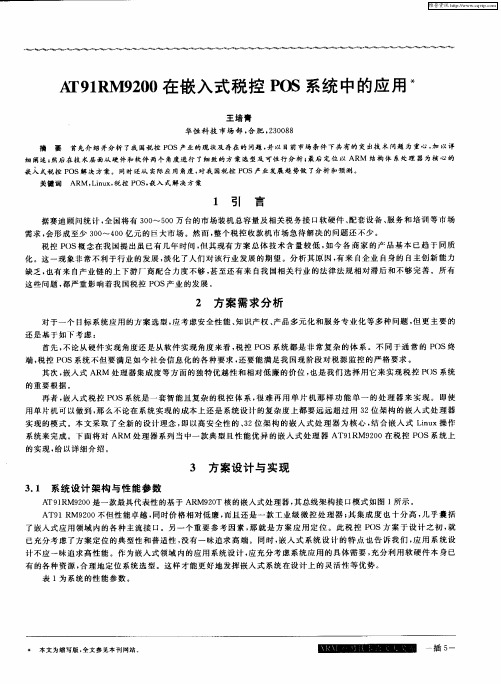
3.1 系统设计架构与性能参数。