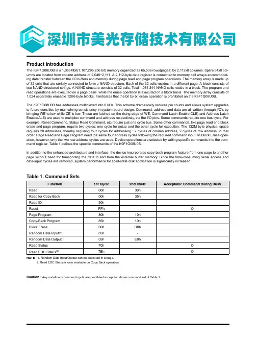
Document Title512M x 8 Bits / 1G x 8 Bits NAND Flash Memory Revision HistoryThe attached data sheets are prepared and approved by SAMSUNG Electronics. SAMSUNG Electronics CO., LTD. reserve the rightto change the specifications. SAMSUNG Electronics will evaluate and reply to your requests and questions about device. If you have any questions, please contact the SAMSUNG branch office near your office.Revision No0.0RemarkAdvanceHistory1. Initial issueDraft DateNov. 15. 2004GENERAL DESCRIPTIONFEATURES• Voltage Supply - 2.70V ~ 3.60V • Organization- Memory Cell Array : (512M + 16,384K)bit x 8bit - Data Register : (2K + 64)bit x 8bit • Automatic Program and Erase - Page Program : (2K + 64)Byte - Block Erase : (128K + 4K)Byte • Page Read Operation- Page Size : (2K + 64)Byte - Random Read : 20µs(Max.) - Serial Access : 25ns(Min.)512M x 8 Bit / 1G x 8 Bits NAND Flash Memory• Fast Write Cycle Time- Page Program time : 200µs(Typ.) - Block Erase Time : 1.5ms(Typ.)• Command/Address/Data Multiplexed I/O Port • Hardware Data Protection- Program/Erase Lockout During Power Transitions • Reliable CMOS Floating-Gate Technology - Endurance : 100K Program/Erase Cycles - Data Retention : 10 Years • Command Driven Operation• Intelligent Copy-Back with internal 1bit/528Byte EDC • Unique ID for Copyright Protection • Package :- K9F4G08U0M-YCB0/YIB048 - Pin TSOP I (12 x 20 / 0.5 mm pitch)- K9F4G08U0M-PCB0/PIB0 : Pb-FREE PACKAGE 48 - Pin TSOP I (12 x 20 / 0.5 mm pitch) - K9F4G08U0M-ICB0/IIB052 - Pin ULGA (12 x 17 / 1.00 mm pitch) - K9K8G08U1M-ICB0/IIB052 - Pin ULGA (12 x 17 / 1.00 mm pitch)Offered in 512Mx8bit, the K9F4G08U0M is a 4G-bit NAND Flash Memory with spare 128M-bit. Its NAND cell provides the most cost-effective solution for the solid state application market. A program operation can be performed in typical 200µs on the (2K+64)Byte page and an erase operation can be performed in typical 1.5ms on a (128K+4K)Byte block. Data in the data page can be read out at 25ns cycle time per Byte. The I/O pins serve as the ports for address and data input/output as well as command input. The on-chip write controller automates all program and erase functions including pulse repetition, where required, and internal verification and margining of data. Even the write-intensive systems can take advantage of the K9F4G08U0M ′s extended reliability of 100K program/erase cycles by providing ECC(Error Correcting Code) with real time mapping-out algorithm. The K9F4G08U0M is an optimum solu-tion for large nonvolatile storage applications such as solid state file storage and other portable applications requiring non-volatility.PRODUCT LISTPart Number Vcc RangeOrganizationPKG Type K9F4G08U0M-Y ,P 2.70 ~ 3.60VX8TSOP1K9F4G08U0M-I 52ULGAK9K8G08U1M-I1.001.001.001.002.007 6 5 4 3 2 11.001.001.0012.00±0.10#A117.00±0.1017.00±0.10BA12.00±0.10(Datum B)(Datum A)12.0010.002.502.502.000.501.30A B C DEF GHJ K L M N12-∅1.00±0.0541-∅0.70±0.05Side View0.65(M a x .)0.10 C17.00±0.10Top ViewBottom ViewABC D EF G H J KL M N7654321PIN CONFIGURATION (ULGA)K9F4G08U0M-ICB0/IIB052-ULGA (measured in millimeters)NCNCNCNCNCNCNCNCNC NC NCNC NCNCNC NCVccVcc VssVssVss /RE NC/CENC CLENC ALE NC /WE NC /WPNC R/B NCVssIO0 NCIO1NCIO2IO3NCNC IO4 NC IO5NCIO6 NCIO7NC∅ABC M 0.1∅ABC M 0.1PACKAGE DIMENSIONS1.001.001.001.002.007 6 5 4 3 2 11.001.001.0012.00±0.10#A117.00±0.1017.00±0.10BA12.00±0.10(Datum B)(Datum A)12.0010.002.502.502.000.501.30A B C DEF GHJ K L M N12-∅1.00±0.0541-∅0.70±0.05Side View0.65(M a x .)0.10 C17.00±0.10Top ViewBottom ViewABC D EF G H J KL M N7654321K9K8G08U1M-ICB0/IIB052-ULGA (measured in millimeters)NCNCNCNCNCNCNCNCNC NCNCNCNCNCNC NCVccVcc VssVssVss /RE1/RE2/CE1/CE2CLE1CLE2ALE1ALE2/WE1/WE2/WP1/WP2R/B1R/B2VssIO0-1IO0-2IO1-1IO1-2IO2-1IO3-1IO2-2IO3-2IO4-1IO4-2IO5-1IO5-2IO6-1IO6-2IO7-1IO7-2∅ABC M 0.1∅ABC M 0.1PACKAGE DIMENSIONSPIN DESCRIPTIONNOTE : Connect all V CC and V SS pins of each device to common power supply outputs. Do not leave V CC or V SS disconnected.Pin Name Pin FunctionI/O 0 ~ I/O 7DATA INPUTS/OUTPUTSThe I/O pins are used to input command, address and data, and to output data during read operations. The I/O pins float to high-z when the chip is deselected or when the outputs are disabled.CLECOMMAND LATCH ENABLEThe CLE input controls the activating path for commands sent to the command register. When active high, commands are latched into the command register through the I/O ports on the rising edge of the WE signal.ALEADDRESS LATCH ENABLEThe ALE input controls the activating path for address to the internal address registers. Addresses are latched on the rising edge of WE with ALE high.CECHIP ENABLEThe CE input is the device selection control. When the device is in the Busy state, CE high is ignored, and the device does not return to standby mode in program or erase operation.REREAD ENABLEThe RE input is the serial data-out control, and when active drives the data onto the I/O bus. Data is valid tREA after the falling edge of RE which also increments the internal column address counter by one.WEWRITE ENABLEThe WE input controls writes to the I/O port. Commands, address and data are latched on the rising edge of the WE pulse.WPWRITE PROTECTThe WP pin provides inadvertent program/erase protection during power transitions. The internal high volt-age generator is reset when the WP pin is active low.R/BREADY/BUSY OUTPUTThe R/B output indicates the status of the device operation. When low, it indicates that a program, erase or random read operation is in process and returns to high state upon completion. It is an open drain output and does not float to high-z condition when the chip is deselected or when outputs are disabled.Vcc POWERV CC is the power supply for device. Vss GROUNDN.CNO CONNECTIONLead is not internally connected.Product IntroductionThe K9F4G08U0M is a 4,224Mbit(4,429,185,024 bit) memory organized as 262,144 rows(pages) by 2,112x8 columns. Spare 64x8 columns are located from column address of 2,048~2,111. A 2,112-byte data register is connected to memory cell arrays accommo-dating data transfer between the I/O buffers and memory during page read and page program operations. The memory array is made up of 32 cells that are serially connected to form a NAND structure. Each of the 32 cells resides in a different page. A block consists of two NAND structured strings. A NAND structure consists of 32 cells. Total 1,081,344 NAND cells reside in a block. The program and read operations are executed on a page basis, while the erase operation is executed on a block basis. The memory array con-sists of 4,096 separately erasable 128K-byte blocks. It indicates that the bit by bit erase operation is prohibited on the K9F4G08U0M. The K9F4G08U0M has addresses multiplexed into 8 I/Os. This scheme dramatically reduces pin counts and allows system upgrades to future densities by maintaining consistency in system board design. Command, address and data are all written through I/O's by bringing WE to low while CE is low. Those are latched on the rising edge of WE. Command Latch Enable(CLE) and Address Latch Enable(ALE) are used to multiplex command and address respectively, via the I/O pins. Some commands require one bus cycle. For example, Reset Command, Status Read Command, etc require just one cycle bus. Some other commands, like page read and block erase and page program, require two cycles: one cycle for setup and the other cycle for execution. The 528M byte physical space requires 30 addresses, thereby requiring five cycles for addressing : 2 cycles of column address, 3 cycles of row address, in that order. Page Read and Page Program need the same five address cycles following the required command input. In Block Erase oper-ation, however, only the three row address cycles are used. Device operations are selected by writing specific commands into the command register. Table 1 defines the specific commands of the K9F4G08U0M.In addition to the enhanced architecture and interface, the device incorporates copy-back program feature from one page to another page without need for transporting the data to and from the external buffer memory. Since the time-consuming serial access and data-input cycles are removed, system performance for solid-state disk application is significantly increased.Table 1. Command SetsFunction1st. Cycle2nd. Cycle Acceptable Command during Busy Read 00h30hRead for Copy Back00h35hRead ID90h-Reset FFh-OPage Program80h10hTwo-Plane Page Program80h---11h81h---10hCopy-Back Program85h10hTwo-Plane Copy-Back Program85h---11h81h---10hBlock Erase60h D0hTwo-Plane Block Erase60h---60h D0hRandom Data Input(1)85h-Random Data Output(1)05h E0hRead Status70h ORead EDC Status(2)7Bh ONOTE : 1. Random Data Input/Output can be executed in a page.2. Read EDC Status is only available on Copy Back operation.Caution : Any undefined command inputs are prohibited except for above command set of Table 1.DC AND OPERATING CHARACTERISTICS (Recommended operating conditions otherwise noted.)NOTE : 1. V IL can undershoot to -0.4V and V IH can overshoot to V CC +0.4V for durations of 20 ns or less. 2. Typical value is measured at Vcc=3.3V, T A =25°C. Not 100% tested.ParameterSymbol Test ConditionsMinTypMaxUnitOperating CurrentPage Read withSerial Access I CC 1tRC=25nsCE=V IL, I OUT =0mA-1530mAProgramI CC 2-EraseI CC 3-Stand-by Current(TTL)I SB 1CE=V IH , WP=0V/V CC --1Stand-by Current(CMOS)I SB 2CE=V CC -0.2, WP=0V/V CC -1050µAInput Leakage Current I LI V IN =0 to Vcc(max)--±10Output Leakage Current I LO V OUT =0 to Vcc(max)--±10Input High VoltageV IH*-0.8xVcc -Vcc+0.3V Input Low Voltage, All inputs V IL*--0.3-0.2xVccOutput High Voltage Level V OH K9F4G08U0M :I OH =-400µA 2.4--Output Low Voltage Level V OL K9F4G08U0M :I OL =2.1mA --0.4Output Low Current(R/B)I OL (R/B)K9F4G08U0M :V OL =0.4V810-mA RECOMMENDED OPERATING CONDITIONS(Voltage reference to GND, K9F4G08U0M-XCB0 :T A =0 to 70°C, K9F4G08U0M-XIB0:T A =-40 to 85°C)ParameterSymbol Min Typ.Max Unit Supply Voltage V CC 2.7 3.3 3.6V Supply VoltageV SSVABSOLUTE MAXIMUM RATINGSNOTE :1. Minimum DC voltage is -0.6V on input/output pins. During transitions, this level may undershoot to -2.0V for periods <30ns. Maximum DC voltage on input/output pins is V CC +0.3V which, during transitions, may overshoot to V CC +2.0V for periods <20ns.2. Permanent device damage may occur if ABSOLUTE MAXIMUM RATINGS are exceeded. Functional operation should be restricted to the conditions as detailed in the operational sections of this data sheet. Exposure to absolute maximum rating conditions for extended periods may affect reliability.ParameterSymbol Rating Unit Voltage on any pin relative to VSS V IN/OUT -0.6 to +4.6V V CC/V CCQ -0.6 to +4.6Temperature Under Bias K9F4G08U0M-XCB0T BIAS -10 to +125°C K9F4G08U0M-XIB0-40 to +125Storage Temperature K9F4G08U0M-XCB0T STG-65 to +150°CK9F4G08U0M-XIB0Short Circuit CurrentI OS5mACAPACITANCE (T A =25°C, V CC =3.3V, f=1.0MHz)NOTE : Capacitance is periodically sampled and not 100% tested.ItemSymbol Test ConditionMin Max Unit Input/Output Capacitance C I/O V IL =0V -10pF Input CapacitanceC INV IN =0V-10pFVALID BLOCKNOTE :1. The device may include invalid blocks when first shipped. Additional invalid blocks may develop while being used. The number of valid blocks is pre-sented with both cases of invalid blocks considered. Invalid blocks are defined as blocks that contain one or more bad bits. Do not erase or programfactory-marked bad blocks. Refer to the attached technical notes for appropriate management of invalid blocks.2. The 1st block, which is placed on 00h block address, is guaranteed to be a valid block, does not require Error Correction up to 1K program/erase cycles.* : Each K9F4G08U0M chip in the K9K8G08U1M has Maximun 80 invalid block.ParameterSymbol Min Typ.Max Unit K9F4G08U0M N VB 4,016-4,096BlocksK9K8G08U1MN VB8,032*-8,192*BlocksAC TEST CONDITION(K9F4G08U0M-XCB0 :T A =0 to 70°C, K9F4G08U0M-XIB0:T A =-40 to 85°C K9F4G08U0M : Vcc=2.7V~3.6V unless otherwise noted)ParameterK9F4G08U0M Input Pulse Levels 0V to Vcc Input Rise and Fall Times 5ns Input and Output Timing Levels Vcc/2Output Load1 TTL GATE and CL=50pFMODE SELECTIONNOTE : 1. X can be V IL or V IH.2. WP should be biased to CMOS high or CMOS low for standby.CLE ALE CE WERE WP ModeH L L H X Read Mode Command Input L H L H X Address Input(5clock)H L L H H Write Mode Command Input L H L H H Address Input(5clock)L L L HH Data Input L L L H X Data Output X X X X H X During Read(Busy)X X X X X H During Program(Busy)X X X X X H DuringErase(Busy)X X (1)X X X L Write Protect XXHXX0V/V CC (2)Stand-byAC Timing Characteristics for Command / Address / Data InputNOTES : 1. The transition of the corresponding control pins must occur only once while WE is held low 2. tADL is the time from the WE rising edge of final address cycle to the WE rising edge of first data cycleParameterSymbol Min Max Unit CLE Setup Time t CLS (1)12-ns CLE Hold Time t CLH 5-ns CE Setup Time t CS (1)20-ns CE Hold Time t CH 5-ns WE Pulse Width t WP 12-ns ALE Setup Time t ALS (1)12-ns ALE Hold Time t ALH 5-ns Data Setup Time t DS (1)12-ns Data Hold Time t DH 5-ns Write Cycle Time t WC 25-ns WE High Hold Time t WH 10-ns ALE to Data Loading Timet ADL (2)70-nsProgram / Erase CharacteristicsNOTE : 1. Typical value is measured at Vcc=3.3V, T A =25°C. Not 100% tested.2. Typical program time is defined as the time that more than 50% of the whole pages are programmed at Vcc of3.3V and temperature of 25°C within.ParameterSymbol Min Typ Max Unit Program Time t PROG (2)-200700µs Dummy Busy Time for Two-Plane Page Program t DBSY -0.51µs Number of Partial Program Cycles in the Same Page Main Array Nop --4cycles Spare Array--4cycles Block Erase Timet BERS- 1.52msAC Characteristics for OperationParameter Symbol Min Max Unit Data Transfer from Cell to Register t R-20µs ALE to RE Delay t AR10-ns CLE to RE Delay t CLR10-ns Ready to RE Low t RR20-ns RE Pulse Width t RP12-ns WE High to Busy t WB-100ns Read Cycle Time t RC25-ns RE Access Time t REA-18ns CE Access Time t CEA-23ns RE High to Output Hi-Z t RHZ-100ns CE High to Output Hi-Z t CHZ-30ns RE High to Output Hold t RHOH15-ns RE Low to Output Hold t RLOH5-ns CE High to Output Hold t COH15-ns RE High Hold Time t REH10-ns Output Hi-Z to RE Low t IR0-ns RE High to WE Low t RHW100-ns WE High to RE Low t WHR60-ns Device Resetting Time(Read/Program/Copy-Back Program/Erase)t RST-5/10/40/500(1)µs NOTE: 1. If reset command(FFh) is written at Ready state, the device goes into Busy for maximum 5us.NAND Flash Technical NotesIdentifying Initial Invalid Block(s)Initial Invalid Block(s)Initial invalid blocks are defined as blocks that contain one or more initial invalid bits whose reliability is not guaranteed by Samsung.The information regarding the initial invalid block(s) is called the initial invalid block information. Devices with initial invalid block(s)have the same quality level as devices with all valid blocks and have the same AC and DC characteristics. An initial invalid block(s)does not affect the performance of valid block(s) because it is isolated from the bit line and the common source line by a select tran-sistor. The system design must be able to mask out the initial invalid block(s) via address mapping. The 1st block, which is placed on 00h block address, is guaranteed to be a valid block, does not require Error Correction up to 1K program/erase cycles.All device locations are erased(FFh) except locations where the initial invalid block(s) information is written prior to shipping. The ini-tial invalid block(s) status is defined by the 1st byte in the spare area. Samsung makes sure that either the 1st or 2nd page of every initial invalid block has non-FFh data at the column address of 2048. Since the initial invalid block information is also erasable in most cases, it is impossible to recover the information once it has been erased. Therefore, the system must be able to recognize the initial invalid block(s) based on the original initial invalid block information and create the initial invalid block table via the following suggested flow chart(Figure 3). Any intentional erasure of the original initial invalid block information is prohibited.*Check "FFh" at the column address 2048 Figure 3. Flow chart to create initial invalid block tableStartSet Block Address = 0Check "FFh"Increment Block AddressLast Block ?EndNoYesYesCreate (or update)NoInitialof the 1st and 2nd page in the blockInvalid Block(s) TableNAND Flash Technical Notes (Continued)Program Flow ChartStartI/O 6 = 1 ?I/O 0 = 0 ?No*Write 80hWrite AddressWrite DataWrite 10hRead Status RegisterProgram Completedor R/B = 1 ?Program ErrorYesNoYes: If program operation results in an error, map out the block including the page in error and copy thetarget data to another block.*Error in write or read operationWithin its life time, additional invalid blocks may develop with NAND Flash memory. Refer to the qualification report for the actual data.The following possible failure modes should be considered to implement a highly reliable system. In the case of status read fail-ure after erase or program, block replacement should be done. Because program status fail during a page program does not affect the data of the other pages in the same block, block replacement can be executed with a page-sized buffer by finding an erased empty block and reprogramming the current target data and copying the rest of the replaced block. In case of Read, ECC must be employed. To improve the efficiency of memory space, it is recommended that the read or verification failure due to single bit error be reclaimed by ECC without any block replacement. The said additional block failure rate does not include those reclaimed blocks.Failure ModeDetection and Countermeasure sequenceWrite Erase Failure Status Read after Erase --> Block Replacement Program Failure Status Read after Program --> Block Replacement ReadSingle Bit FailureVerify ECC -> ECC CorrectionECC: Error Correcting Code --> Hamming Code etc. Example) 1bit correction & 2bit detectionNAND Flash Technical Notes (Continued)Copy-Back Operation with EDC & Plane Definition for EDCGenerally, copy-back program is very powerful to move data stored in a page without utilizing any external memory. But, if the source page has a bit error for charge loss or charge gain, accumulated copy-back operations could also accumulate bit errors. For this rea-son, two-bit ECC is recommanded for copy-back operation.Because K9F4G08U0M supports Copy Back with EDC operation, only 1-bit ECC is sufficient for copy-back operation. During Copy-Back operation, the system controller can detect a bit error for each 528-byte plane by monitoring the Status bits (I/O1 & I/O 2) of the Status Register.There are some restrictions against programming unit in copy-back operation with EDC. For enabling EDC operation, the page pro-gram should be performed with the whole page unit (2,112-byte) or the each 528-byte plane unit. A page of 2,112-byte is composed of 4 planes of 528-byte and each 528-byte plane is made up of 512-byte in the main area and 16-byte in the spare area."A" area 512 Byte(1’st plane)"H" area (4’th plane)Main Area (2,048 Byte)16 Byte"G" area (3’rd plane)16 Byte "F" area (2’nd plane)16 Byte "E" area (1’st plane)16 Byte "B" area 512 Byte(2’nd plane)"C" area 512 Byte(3’rd plane)"D" area 512 Byte(4’th plane)Spare Area (64 Byte)Table 2. Definition of the 528-Byte PlanePlane Main Area (Column 0~2,047)Spare Area (Column 2,048~2,111)Area NameColumn AddressArea NameColumn Address 1’st 528-Byte Plane "A"0 ~ 511"E"2,048 ~ 2,0632’nd 528-Byte Plane "B"512 ~ 1,023"F"2,064 ~ 2,0793’rd 528-Byte Plane "C"1,024 ~ 1,535"G"2,080 ~ 2,0954’th 528-Byte Plane"D"1,536 ~ 2,047"H"2,096 ~ 2,111Within a block, the pages must be programmed consecutively from the LSB (least significant bit) page of the block to MSB (most sig-nificant bit) pages of the block. Random page address programming is prohibited.From the LSB page to MSB page DATA IN: Data (1)Data (64)(1)(2)(3)(32)(64)Data register Page 0Page 1Page 2Page 31Page 63Ex.) Random page program (Prohibition)DATA IN: Data (1)Data (64)(2)(32)(3)(1)(64)Data registerPage 0Page 1Page 2Page 31Page 63Addressing for program operation::::Read ID OperationCECLEWEALERE90hRead ID CommandMaker Code Device Code00h EChDevice t REAAddress 1cycle4th cyc.*I/Oxt ARDevice Device Code*(2nd Cycle)3rd Cycle*4th Cycle*K9F4G08U0M DCh10h95hK9K8G08U1MSame as each K9F4G08U0M in itCode*3rd cyc.*4th ID DataDescription I/O7 I/O6I/O5 I/O4 I/O3I/O2I/O1 I/O0Page Size(w/o redundant area ) 1KB2KBReservedReserved0 00 11 01 1Block Size(w/o redundant area ) 64KB128KB256KBReserved0 00 11 01 1Redundant Area Size ( byte/512byte) 8161Organization x8x161Serial AccessMinimum 50ns25nsReservedReserved1111ID Definition Table90 ID : Access command = 90HDescription1st Byte 2nd Byte 3rd Byte 4th Byte Maker CodeDevice CodeInternal Chip Number, Cell Type, Number of Simultaneously Programed Pages, Etc Page Size, Block Size,Redundant Area Size, Organization, Serial Access Minimum3rd ID DataDescription I/O7 I/O6I/O5 I/O4I/O3 I/O2I/O1 I/O0Internal Chip Number 12480 00 11 01 1Cell Type 2 Level Cell4 Level Cell8 Level Cell16 Level Cell0 00 11 01 1Number ofSimultaneouslyProgrammed Pages 12480 00 11 01 1Interleave Program Between multiple chips Not SupportSupport1Cache Program Not SupportSupport1Figure 7. Random Data Output In a PageAddress 00hData OutputR/B RE t R30hAddress 05hE0h5Cycles2Cycles Data OutputData Field Spare Field Data Field Spare FieldI/OxCol. Add.1,2 & Row Add.1,2,3PAGE PROGRAMThe device is programmed basically on a page basis, but it does allow multiple partial page programing of a word or consecutive bytes up to 2,112, in a single page program cycle. The number of consecutive partial page programming operation within the same page without an intervening erase operation must not exceed 4 times for main array(1time/512byte) and 4 times for spare array(1time/16byte). The addressing should be done in sequential order in a block. A page program cycle consists of a serial data loading period in which up to 2,112bytes of data may be loaded into the data register, followed by a non-volatile programming period where the loaded data is programmed into the appropriate cell.The serial data loading period begins by inputting the Serial Data Input command(80h), followed by the five cycle address inputs and then serial data loading. The words other than those to be programmed do not need to be loaded. The device supports random data input in a page. The column address for the next data, which will be entered, may be changed to the address which follows random data input command(85h). Random data input may be operated multiple times regardless of how many times it is done in a page.The Page Program confirm command(10h) initiates the programming process. Writing 10h alone without previously entering the serial data will not initiate the programming process. The internal write state controller automatically executes the algorithms and tim-ings necessary for program and verify, thereby freeing the system controller for other tasks. Once the program process starts, the Read Status Register command may be entered to read the status register. The system controller can detect the completion of a pro-gram cycle by monitoring the R/B output, or the Status bit(I/O 6) of the Status Register. Only the Read Status command and Reset command are valid while programming is in progress. When the Page Program is complete, the Write Status Bit(I/O 0) may be checked(Figure 8). The internal write verify detects only errors for "1"s that are not successfully programmed to "0"s. The command register remains in Read Status command mode until another valid command is written to the command register.Figure 8. Program & Read Status Operation80hR/B Address & Data Input I/O 0PassData10h70hFailt PROGI/OxCol. Add.1,2 & Row Add.1,2,3"0""1"Col. Add.1,2Figure 9. Random Data Input In a Page80hR/B Address & Data Input I/O 0Pass10h 70h Failt PROG85h Address & Data InputI/OxCol. Add.1,2 & Row Add1,2,3Col. Add.1,2 DataData"0""1"Copy-Back ProgramThe Copy-Back program is configured to quickly and efficiently rewrite data stored in one page without utilizing an external memory.Since the time-consuming cycles of serial access and re-loading cycles are removed, the system performance is improved. The ben-efit is especially obvious when a portion of a block is updated and the rest of the block also need to be copied to the newly assigned free block. The operation for performing a copy-back program is a sequential execution of page-read without serial access and copy-ing-program with the address of destination page. A read operation with "35h" command and the address of the source page moves the whole 2,112-byte data into the internal data buffer. As soon as the device returns to Ready state, Page-Copy Data-input com-mand (85h) with the address cycles of destination page followed may be written. The Program Confirm command (10h) is required to actually begin the programming operation. During tPROG, the device executes EDC of itself. Once the program process starts, the Read Status Register command (70h) or Read EDC Status command (7Bh) may be entered to read the status register. The system controller can detect the completion of a program cycle by monitoring the R/B output, or the Status bit(I/O 6) of the Status Register.When the Copy-Back Program is complete, the Write Status Bit(I/O 0) and EDC Status Bits (I/O 1 ~ I/O 4) may be checked(Figure 10& Figure 11& Figure 12). The internal write verification detects only errors for "1"s that are not successfully programmed to "0"s and the internal EDC checks whether there is only 1-bit error for each 528-byte plane of the source page. More than 2-bit error detection is not available for each 528-byte plane. The command register remains in Read Status command mode or Read EDC Status com-mand mode until another valid command is written to the command register.During copy-back program, data modification is possible using random data input command (85h) as shown in Figure11. But EDC status Bits are not available during copy back for some bits or bytes modified by Random Data Input operation. However, in case of the 528 byte plane unit modification, EDC status bits are abailable.Figure 10. Page Copy-Back program Operation00hR/B Add.(5Cycles)I/O 0Pass85h 70h Failt PROGAdd.(5Cycles) t R Source Address Destination Address35h10h I/OxCol. Add.1,2 & Row Add.1,2,3Col. Add.1,2 & Row Add.1,2,3Figure 11. Page Copy-Back program Operation with Random Data Input00hR/B Add.(5Cycles)85h 70ht PROGAdd.(5Cycles) t RSource AddressDestination AddressData 35h10h 85hData Add.(2Cycles) There is no limitation for the number of repetition.I/OxCol. Add.1,2 & Row Add.1,2,3Col. Add.1,2 & Row Add.1,2,3Col. Add.1,2Note: 1. For EDC operation, only one time random data input is possible at the same address.Note : 1. Copy-Back Program operation is allowed only within the same memory plane.2. On the same plane, It’s prohibited to operate copy-back program from an odd address page(source page) to an even address page(target page) or from an even address page(source page) to an odd address page(target page). Therefore, the copy-back program is permitted just between odd address pages or even address pages.。