
MBM29F040A-12中文资料
- 格式:pdf
- 大小:723.37 KB
- 文档页数:18

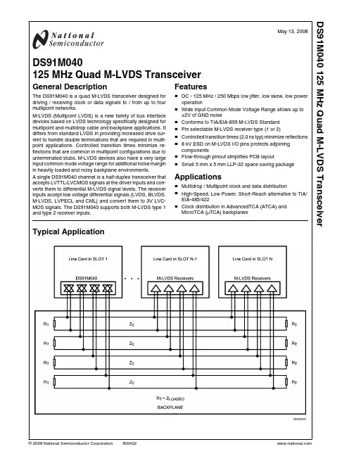
May 13, 2008 DS91M040125 MHz Quad M-LVDS TransceiverGeneral DescriptionThe DS91M040 is a quad M-LVDS transceiver designed for driving / receiving clock or data signals to / from up to four multipoint networks.M-LVDS (Multipoint LVDS) is a new family of bus interface devices based on LVDS technology specifically designed for multipoint and multidrop cable and backplane applications. It differs from standard LVDS in providing increased drive cur-rent to handle double terminations that are required in multi-point applications. Controlled transition times minimize re-flections that are common in multipoint configurations due to unterminated stubs. M-LVDS devices also have a very large input common mode voltage range for additional noise margin in heavily loaded and noisy backplane environments.A single DS91M040 channel is a half-duplex transceiver that accepts LVTTL/LVCMOS signals at the driver inputs and con-verts them to differential M-LVDS signal levels. The receiver inputs accept low voltage differential signals (LVDS, BLVDS, M-LVDS, LVPECL and CML) and convert them to 3V LVC-MOS signals. The DS91M040 supports both M-LVDS type 1 and type 2 receiver inputs.Features■DC - 125 MHz / 250 Mbps low jitter, low skew, low power operation■Wide Input Common Mode Voltage Range allows up to ±2V of GND noise■Conforms to TIA/EIA-899 M-LVDS Standard■Pin selectable M-LVDS receiver type (1 or 2)■Controlled transition times (2.0 ns typ) minimize reflections ■8 kV ESD on M-LVDS I/O pins protects adjoining components■Flow-through pinout simplifies PCB layout■Small 5 mm x 5 mm LLP-32 space saving package Applications■Multidrop / Multipoint clock and data distribution■High-Speed, Low Power, Short-Reach alternative to TIA/ EIA-485/422■Clock distribution in AdvancedTCA (ATCA) and MicroTCA (μTCA) backplanesTypical Application30042202© 2008 National Semiconductor DS91M040 125 MHz Quad M-LVDS TransceiverOrdering InformationOrder Number Receiver Input FunctionPackage TypeDS91M040TSQType 1 or 2Quad M-LVDS TranscieverLLP-32Connection Diagram30042201Logic Diagram30042203 2D S 91M 040Pin DescriptionsNumber Name I/O, Type Description1, 3, 5, 7RO O, LVCMOS Receiver output pin.26, 28, 13, 15RE I, LVCMOS Receiver enable pin: When RE is high, the receiver is disabled.When RE is low, the receiver is enabled. There is a 300 kΩ pullupresistor on this pin.25, 27, 14, 16DE I, LVCMOS Driver enable pin: When DE is low, the driver is disabled. WhenDE is high, the driver is enabled. There is a 300 kΩ pulldownresistor on this pin.2, 4, 6, 8DI I, LVCMOS Driver input pin.31, DAP GND Power Ground pin and pad.17, 19, 21, 23A I/O, M-LVDS Non-inverting driver output pin/Non-inverting receiver input pin 18, 20, 22, 24B I/O, M-LVDS Inverting driver output pin/Inverting receiver input pin11, 12, 29, 30VDDPower Power supply pin, +3.3V ± 0.3V32FSEN1I, LVCMOS Failsafe enable pin with a 300 kΩ pullup resistor. This pinenables Type 2 receiver on inputs 0 and 2.FSEN1 = L --> Type 1 receiver inputsFSEN1 = H --> Type 2 receiver inputs9FSEN2I, LVCMOS Failsafe enable pin with a 300 kΩ pullup resistor. This pinenables Type 2 receiver on inputs 1 and 3.FSEN2 = L --> Type 1 receiver inputsFSEN2 = H --> Type 2 receiver inputs10MDE I, LVCMOS Master enable pin. When MDE is H, the device is powered up.When MDE is L, the device overrides all other control and powersdown.M-LVDS Receiver TypesThe EIA/TIA-899 M-LVDS standard specifies two differenttypes of receiver input stages. A type 1 receiver has a con-ventional threshold that is centered at the midpoint of the inputamplitude, VID /2. A type 2 receiver has a built in offset that is100mV greater then VID /2. The type 2 receiver offset acts asa failsafe circuit where open or short circuits at the input willalways result in the output stage being driven to a low logicstate.30042240FIGURE 1. M-LVDS Receiver Input Thresholds DS91M040Absolute Maximum Ratings (Note 4)If Military/Aerospace specified devices are required,please contact the National Semiconductor Sales Office/Distributors for availability and specifications.Power Supply Voltage −0.3V to +4V LVCMOS Input Voltage −0.3V to (V DD + 0.3V)LVCMOS Output Voltage −0.3V to (V DD + 0.3V)M-LVDS I/O Voltage −5.5V to +5.5V M-LVDS Output Short Circuit Current Duration Continuous Junction Temperature +140°C Storage Temperature Range −65°C to +150°C Lead Temperature Range Soldering (4 sec.)+260°C Maximum Package Power Dissipation @ +25°C SQ Package 833 mW Derate SQ Package 6.67 mW/°C above +25°C Package Thermal Resistance θJA +150°C/W θJC +63.8°C/WESD Susceptibility HBM (Note 1)≥8 kV MM (Note 2)≥250V CDM (Note 3)≥1250VNote 1:Human Body Model, applicable std. JESD22-A114C Note 2:Machine Model, applicable std. JESD22-A115-A Note 3:Field Induced Charge Device Model, applicable std.JESD22-C101-CRecommended Operating ConditionsMin Typ Max Units Supply Voltage, V DD3.0 3.3 3.6V Voltage at Any Bus Terminal−1.4 +3.8V (Separate or Common-Mode)Differential Input Voltage V ID 2.4V LVTTL Input Voltage High V IH 2.0 V DD V LVTTL Input Voltage Low V IL 0 0.8V Operating Free Air Temperature T A −40+25+85°CDC Electrical Characteristics(Notes 5, 6, 7, 9)Over recommended operating supply and temperature ranges unless otherwise specified.Symbol ParameterConditionsMin Typ Max Units M-LVDS Driver |V AB |Differential output voltage magnitudeR L = 50Ω, C L = 5 pF 480 650mV ΔV AB Change in differential output voltage magnitude between logic statesFigures 2, 4−500+50mV V OS(SS)Steady-state common-mode output voltageR L = 50Ω, C L = 5 pF 0.3 1.6 2.1V |ΔV OS(SS)|Change in steady-state common-mode outputvoltage between logic states Figures 2, 30 +50mV V A(OC)Maximum steady-state open-circuit output voltage Figure 50 2.4V V B(OC)Maximum steady-state open-circuit output voltage0 2.4V V P(H)Voltage overshoot, low-to-high level output (Note 12)R L = 50Ω, C L = 5pF, C D = 0.5 pF Figures 7, 81.2V SSV V P(L)Voltage overshoot, high-to-low level output (Note 12)−0.2V SSV I IH High-level input current (LVTTL inputs)V IH = 2.0V -15 15μA I IL Low-level input current (LVTTL inputs)V IL = 0.8V -15 15μA V CL Input Clamp Voltage (LVTTL inputs)I IN = -18 mA -1.5 V I OS Differential short-circuit output current (Note 8)Figure 6-43 43mA M-LVDS ReceiverV IT+Positive-going differential input voltage threshold See Function Tables Type 1 1650mV Type 2 100150mV V IT−Negative-going differential input voltage threshold See Function Tables Type 1−5020 mV Type 25094 mV V OH High-level output voltage (LVTTL output)I OH = −8mA 2.4 2.7 V V OL Low-level output voltage (LVTTL output)I OL = 8mA 0.280.4V I OZ TRI-STATE output currentV O = 0V or 3.6V−10 10μA I OSRShort-circuit receiver output current (LVTTL output)V O = 0V-50-90mA 4D S 91M 040Symbol ParameterConditionsMin Typ Max Units M-LVDS Bus (Input and Output) PinsI ATransceiver input/output currentV A = 3.8V, V B = 1.2V 32µA V A = 0V or 2.4V, V B = 1.2V −20 +20µA V A = −1.4V, V B = 1.2V−32 µA I BTransceiver input/output currentV B = 3.8V, V A = 1.2V 32µA V B = 0V or 2.4V, V A = 1.2V −20 +20µA V B = −1.4V, V A = 1.2V−32 µA I AB Transceiver input/output differential current (I A − I B )V A = V B , −1.4V ≤ V ≤ 3.8V −4 +4µA I A(OFF)Transceiver input/output power-off currentV A = 3.8V, V B = 1.2V,DE = V CC = 1.5V32µA V A = 0V or 2.4V, V B = 1.2V,DE = V CC = 1.5V −20 +20µA V A = −1.4V, V B = 1.2V,DE = V CC = 1.5V−32 µA I B(OFF)Transceiver input/output power-off currentV B = 3.8V, V A = 1.2V,DE = V CC = 1.5V32µA V B = 0V or 2.4V, V A = 1.2V,DE = V CC = 1.5V −20 +20µA V B = −1.4V, V A = 1.2V,DE = V CC = 1.5V−32 µA I AB(OFF)Transceiver input/output power-off differential current (I A(OFF) − I B(OFF))V A = V B , −1.4V ≤ V ≤ 3.8V,V DD = 1.5V, DE = 1.5V −4 +4µA C A Transceiver input/output capacitance V DD = OPEN7.8 pF C B Transceiver input/output capacitance7.8 pF C AB Transceiver input/output differential capacitance 3 pF C A/BTransceiver input/output capacitance balance (C A /C B )1SUPPLY CURRENT (V CC )I CCD Driver Supply Current R L = 50Ω, DE = H, RE = H 6775mA I CCZ TRI-STATE Supply Current DE = L, RE = H 2226mA I CCR Receiver Supply Current DE = L, RE = L 3238mA I CCPDPower Down Supply CurrentMDE = L35mANote 4:“Absolute Maximum Ratings” indicate limits beyond which damage to the device may occur, including inoperability and degradation of device reliability and/or performance. Functional operation of the device and/or non-degradation at the Absolute Maximum Ratings or other conditions beyond those indicated in the Recommended Operating Conditions is not implied. The Recommended Operating Conditions indicate conditions at which the device is functional and the device should not be operated beyond such conditions.Note 5:The Electrical Characteristics tables list guaranteed specifications under the listed Recommended Operating Conditions except as otherwise modified or specified by the Electrical Characteristics Conditions and/or Notes. Typical specifications are estimations only and are not guaranteed.Note 6:Current into device pins is defined as positive. Current out of device pins is defined as negative. All voltages are referenced to ground except V OD and ΔV OD .Note 7:Typical values represent most likely parametric norms for V DD = +3.3V and T A = +25°C, and at the Recommended Operation Conditions at the time of product characterization and are not guaranteed.Note 8:Output short circuit current (I OS ) is specified as magnitude only, minus sign indicates direction only.Note 9:C L includes fixture capacitance and C D includes probe capacitance.DS91M040Switching Characteristics(Notes 10, 11, 17)Over recommended operating supply and temperature ranges unless otherwise specified.SymbolParameterConditionsMin Typ Max Units DRIVER AC SPECIFICATIONS t PLH Differential Propagation Delay Low to High R L = 50Ω, C L = 5 pF, 1.5 3.3 5.5ns t PHL Differential Propagation Delay High to Low C D = 0.5 pF 1.5 3.3 5.5ns t SKD1Pulse Skew (Notes 12, 13)Figures 7, 8 30125ps t SKD2Channel-to-Channel Skew (Notes 12, 14) 100200ps t SKD3Part-to-Part Skew (Notes 12, 15) 0.8 1.6ns t SKD4Part-to-Part Skew (Notes 12, 16) 4ns t TLH Rise Time (Note 12)1.22.03.0ns t THL Fall Time (Note 12)1.22.03.0ns t PZH Enable Time (Z to Active High)R L = 50Ω, C L = 5 pF, 7.511.5ns t PZL Enable Time (Z to Active Low )C D = 0.5 pF 8.011.5ns t PLZ Disable Time (Active Low to Z)Figures 9, 10 7.011.5ns t PHZ Disable Time (Active High to Z)7.011.5ns RECEIVER AC SPECIFICATIONSt PLH Propagation Delay Low to High C L = 15 pF 1.5 3.0 4.5ns t PHL Propagation Delay High to Low Figures 11, 12, 13 1.5 3.1 4.5ns t SKD1A Pulse Skew (Receiver Type 1)(Notes 12, 13)55325ps t SKD1B Pulse Skew (Receiver Type 2)(Notes 12, 13)475800ps t SKD2Channel-to-Channel Skew (Notes 12, 14) 60300ps t SKD3Part-to-Part Skew (Notes 12, 15) 0.6 1.2ns t SKD4Part-to-Part Skew (Notes 12, 16) 3ns t TLH Rise Time (Note 12) 0.3 1.1 1.6ns t THL Fall Time (Note 12)0.30.65 1.6ns t PZH Enable Time (Z to Active High)R L = 500Ω, C L = 15 pF 3 5.5ns t PZL Enable Time (Z to Active Low)Figures 14, 15 3 5.5ns t PLZ Disable Time (Active Low to Z) 3.5 5.5ns t PHZ Disable Time (Active High to Z) 3.5 5.5ns GENERIC AC SPECIFICATIONSt WKUP Wake Up Time (Note 12)(Master Device Enable (MDE) time) 500ms f MAXMaximum Operating Frequency (Note 12)125MHzNote 10:The Electrical Characteristics tables list guaranteed specifications under the listed Recommended Operating Conditions except as otherwise modified or specified by the Electrical Characteristics Conditions and/or Notes. Typical specifications are estimations only and are not guaranteed.Note 11:Typical values represent most likely parametric norms for V DD = +3.3V and T A = +25°C, and at the Recommended Operation Conditions at the time of product characterization and are not guaranteed.Note 12:Specification is guaranteed by characterization and is not tested in production.Note 13:t SKD1, |t PLHD − t PHLD |, Pulse Skew, is the magnitude difference in differential propagation delay time between the positive going edge and the negative going edge of the same channel.Note 14:t SKD2, Channel-to-Channel Skew, is the difference in propagation delay (t PLHD or t PHLD ) among all output channels.Note 15:t SKD3, Part-to-Part Skew, is defined as the difference between the minimum and maximum differential propagation delays. This specification applies to devices at the same V DD and within 5°C of each other within the operating temperature range.Note 16:t SKD4, Part-to-Part Skew, is the differential channel-to-channel skew of any event between devices. This specification applies to devices over recommended operating temperature and voltage ranges, and across process distribution. t SKD4 is defined as |Max − Min| differential propagation delay.Note 17:C L includes fixture capacitance and C D includes probe capacitance.Note 18:Measured on a clock edge with a histogram and an acummulation of 1500 histogram hits. Input stimulus jitter is subracted geometrically. 6D S 91M 040Test Circuits and Waveforms30042214FIGURE 2. Differential Driver Test Circuit30042224FIGURE 3. Differential Driver Waveforms30042222FIGURE 4. Differential Driver Full Load Test Circuit30042212FIGURE 5. Differential Driver DC Open Test CircuitDS91M04030042225FIGURE 6. Differential Driver Short-Circuit Test Circuit30042216FIGURE 7. Driver Propagation Delay and Transition Time Test Circuit30042218FIGURE 8. Driver Propagation Delays and Transition Time Waveforms 8D S 91M 04030042219FIGURE 9. Driver TRI-STATE Delay Test Circuit30042221FIGURE 10. Driver TRI-STATE Delay Waveforms30042215FIGURE 11. Receiver Propagation Delay and Transition Time Test Circuit DS91M04030042217FIGURE 12. Type 1 Receiver Propagation Delay and Transition Time Waveforms30042223FIGURE 13. Type 2 Receiver Propagation Delay and Transition Time Waveforms30042213FIGURE 14. Receiver TRI-STATE Delay Test Circuit 10D S 91M 040DS91M04030042220FIGURE 15. Receiver TRI-STATE Delay WaveformsTruth TablesDS91M040 Transmitting InputsOutputsRE DE DI B A X H H L H X H L H L XLXZZX — Don't care condition Z — High impedance stateDS91M040 as Type 1 ReceivingInputsOutput FSEN RE DE A − BRO L L L ≥ +0.05V H L L L ≤ −0.05VL L L L 0V X LHLXZX — Don't care condition Z — High impedance state DS91M040 as Type 2 ReceivingInputs Output FSEN RE DE A − BR H L L ≥ +0.15V H H L L ≤ +0.05VL H L L 0V L HHLXZX — Don't care condition Z — High impedance stateDS91M040 Type 1 Receiver Input Threshold Test VoltagesApplied Voltages Resulting Differential InputVoltageResulting Common-ModeInput VoltageReceiver OutputV IA V IB V ID V ICM R 2.400V 0.000V 2.400V 1.200V H 0.000V 2.400V −2.400V 1.200V L 3.800V 3.750V 0.050V 3.775V H 3.750V 3.800V −0.050V 3.775V L −1.350V −1.400V 0.050V −1.375V H −1.400V−1.350V−0.050V−1.375VLH — High Level L — Low LevelOutput state assumes that the receiver is enabled (RE = L)DS91M040 Type 2 Receiver Input Threshold Test VoltagesApplied Voltages Resulting Differential InputVoltageResulting Common-ModeInput VoltageReceiver OutputV IA V IB V ID V IC R 2.400V 0.000V 2.400V 1.200V H 0.000V 2.400V −2.400V 1.200V L 3.800V 3.650V 0.150V 3.725V H 3.800V 3.750V 0.050V 3.775V L −1.250V −1.400V 0.150V −1.325V H −1.350V−1.400V0.050V−1.375VLH — High Level L — Low LevelOutput state assumes that the receiver is enabled (RE = L) 12D S 91M 040Typical Performance30042250 Driver Rise Time as a Function of Temperature30042251 Driver Fall Time as a Function of Temperature30042258 Driver Output Signal Amplitude as a Function ofResistive Load30042252Driver Propagation Delay (tPLHD) as a Function ofTemperature30042253Driver Propagation Delay (tPHLD) as a Function ofTemperatureDS91M04030042254Driver Power Supply Current as a Function of Frequency30042255Receiver Power Supply Current as a Function ofFrequency30042256Receiver Propagation Delay (tPLHD) as a Function ofInput Common Mode Voltage30042257Receiver Propagation Delay (tPHLD) as a Function ofInput Common Mode Voltage 14D S 91M 040Physical Dimensions inches (millimeters) unless otherwise notedOrder Number DS91M040TSQSee NS package Number SQA32A(See AN-1187 for PCB Design and Assembly Recommendations) DS91M040NotesD S 91M 040 125 M H z Q u a d M -L V D S T r a n s c e i v e rFor more National Semiconductor product information and proven design tools, visit the following Web sites at:ProductsDesign SupportAmplifiers /amplifiers WEBENCH /webench Audio/audio Analog University /AU Clock Conditioners /timing App Notes /appnotes Data Converters /adc Distributors /contacts Displays /displays Green Compliance /quality/green Ethernet /ethernet Packaging/packaging Interface /interface Quality and Reliability /quality LVDS/lvds Reference Designs /refdesigns Power Management /power Feedback /feedback Switching Regulators /switchers LDOs /ldo LED Lighting /led PowerWise/powerwise Serial Digital Interface (SDI)/sdiTemperature Sensors /tempsensors Wireless (PLL/VCO)/wirelessTHE CONTENTS OF THIS DOCUMENT ARE PROVIDED IN CONNECTION WITH NATIONAL SEMICONDUCTOR CORPORATION (“NATIONAL”) PRODUCTS. NATIONAL MAKES NO REPRESENTATIONS OR WARRANTIES WITH RESPECT TO THE ACCURACY OR COMPLETENESS OF THE CONTENTS OF THIS PUBLICATION AND RESERVES THE RIGHT TO MAKE CHANGES TO SPECIFICATIONS AND PRODUCT DESCRIPTIONS AT ANY TIME WITHOUT NOTICE. NO LICENSE, WHETHER EXPRESS,IMPLIED, ARISING BY ESTOPPEL OR OTHERWISE, TO ANY INTELLECTUAL PROPERTY RIGHTS IS GRANTED BY THIS DOCUMENT.TESTING AND OTHER QUALITY CONTROLS ARE USED TO THE EXTENT NATIONAL DEEMS NECESSARY TO SUPPORT NATIONAL’S PRODUCT WARRANTY. EXCEPT WHERE MANDATED BY GOVERNMENT REQUIREMENTS, TESTING OF ALL PARAMETERS OF EACH PRODUCT IS NOT NECESSARILY PERFORMED. NATIONAL ASSUMES NO LIABILITY FOR APPLICATIONS ASSISTANCE OR BUYER PRODUCT DESIGN. BUYERS ARE RESPONSIBLE FOR THEIR PRODUCTS AND APPLICATIONS USING NATIONAL COMPONENTS. PRIOR TO USING OR DISTRIBUTING ANY PRODUCTS THAT INCLUDE NATIONAL COMPONENTS, BUYERS SHOULD PROVIDE ADEQUATE DESIGN, TESTING AND OPERATING SAFEGUARDS.EXCEPT AS PROVIDED IN NATIONAL’S TERMS AND CONDITIONS OF SALE FOR SUCH PRODUCTS, NATIONAL ASSUMES NO LIABILITY WHATSOEVER, AND NATIONAL DISCLAIMS ANY EXPRESS OR IMPLIED WARRANTY RELATING TO THE SALE AND/OR USE OF NATIONAL PRODUCTS INCLUDING LIABILITY OR WARRANTIES RELATING TO FITNESS FOR A PARTICULAR PURPOSE, MERCHANTABILITY, OR INFRINGEMENT OF ANY PATENT, COPYRIGHT OR OTHER INTELLECTUAL PROPERTY RIGHT.LIFE SUPPORT POLICYNATIO NAL’S PRO DUCTS ARE NO T AUTHO RIZED FO R USE AS CRITICAL CO MPO NENTS IN LIFE SUPPO RT DEVICES O R SYSTEMS WITHO UT THE EXPRESS PRIO R WRITTEN APPRO VAL O F THE CHIEF EXECUTIVE O FFICER AND GENERAL COUNSEL OF NATIONAL SEMICONDUCTOR CORPORATION. As used herein:Life support devices or systems are devices which (a) are intended for surgical implant into the body, or (b) support or sustain life and whose failure to perform when properly used in accordance with instructions for use provided in the labeling can be reasonably expected to result in a significant injury to the user. A critical component is any component in a life support device or system whose failure to perform can be reasonably expected to cause the failure of the life support device or system or to affect its safety or effectiveness.National Semiconductor and the National Semiconductor logo are registered trademarks of National Semiconductor Corporation. All other brand or product names may be trademarks or registered trademarks of their respective holders.Copyright© 2008 National Semiconductor CorporationFor the most current product information visit us at National Semiconductor Americas Technical Support CenterEmail: support@ Tel: 1-800-272-9959National Semiconductor Europe Technical Support CenterEmail: europe.support@ German Tel: +49 (0) 180 5010 771English Tel: +44 (0) 870 850 4288National Semiconductor Asia Pacific Technical Support Center Email: ap.support@National Semiconductor Japan Technical Support Center Email: jpn.feedback@。

LM78M12中⽂资料LM341/LM78MXX Series3-Terminal Positive Voltage RegulatorsGeneral DescriptionThe LM341and LM78MXX series of three-terminal positive voltage regulators employ built-in current limiting,thermal shutdown,and safe-operating area protection which makes them virtually immune to damage from output overloads.With adequate heatsinking,they can deliver in excess of 0.5A output current.Typical applications would include local (on-card)regulators which can eliminate the noise and de-graded performance associated with single-point regulation.Featuresn Output current in excess of 0.5A n No external componentsn Internal thermal overload protection n Internal short circuit current-limitingn Output transistor safe-area compensationnAvailable in TO-220,TO-39,and TO-252D-PAK packagesn Output voltages of 5V,12V,and 15VConnection DiagramsTO-39Metal Can Package (H)DS010484-5Bottom ViewOrder Number LM78M05CH,LM78M12CH or LM78M15CHSee NS Package Number H03ATO-220Power Package (T)DS010484-6Top ViewOrder Number LM341T-5.0,LM341T-12,LM341T-15,LM78M05CT,LM78M12CT or LM78M15CTSee NS Package Number T03BTO-252DS010484-19Top ViewOrder Number LM78M05CDT See NS Package Number TD03BJuly 1999LM341/LM78MXX Series 3-Terminal Positive Voltage Regulators1999National Semiconductor Corporation /doc/96ef4d46852458fb770b5641.htmlAbsolute Maximum Ratings(Note1)If Military/Aerospace specified devices are required, please contact the National Semiconductor Sales Office/ Distributors for availability and specifications.Lead Temperature(Soldering,10seconds)TO-39Package(H)300?C TO-220Package(T)260?C Storage Temperature Range?65?C to+150?C Operating Junction TemperatureRange?40?C to+125?C Power Dissipation(Note2)Internally Limited Input Voltage5V≤V O≤15V35V ESD Susceptibility TBDElectrical CharacteristicsLimits in standard typeface are for T J=25?C,and limits in boldface type apply over the?40?C to+125?C operating temperature range.Limits are guaranteed by production testing or correlation techniques using standard Statistical Quality Control(SQC) methods.LM341-5.0,LM78M05CUnless otherwise specified:V IN=10V,C IN=0.33µF,C O=0.1µFSymbol Parameter Conditions Min Typ Max Units V O Output Voltage I L=500mA 4.8 5.0 5.2V5mA≤I L≤500mA 4.75 5.0 5.25P D≤7.5W,7.5V≤V IN≤20VV R LINE Line Regulation7.2V≤V IN≤25V I L=100mA50mVI L=500mA100V R LOAD Load Regulation5mA≤I L≤500mA100I Q Quiescent Current I L=500mA410.0mA ?I Q Quiescent Current Change5mA≤I L≤500mA0.57.5V≤V IN≤25V,I L=500mA 1.0V n Output Noise Voltage f=10Hz to100kHz40µVElectrical CharacteristicsLimits in standard typeface are for T J=25?C,and limits in boldface type apply over the?40?C to+125?C operating temperature range.Limits are guaranteed by production testing or correlation techniques using standard Statistical Quality Control(SQC) methods.(Continued)LM341-12,LM78M12CUnless otherwise specified:V IN=19V,C IN=0.33µF,C O=0.1µFSymbol Parameter Conditions Min Typ Max UnitsV O Output Voltage I L=500mA11.51212.5V5mA≤I L≤500mA11.41212.6P D≤7.5W,14.8V≤V IN≤27VV R LINE Line Regulation14.5V≤V IN≤30V I L=100mA120mVI L=500mA240V R LOAD Load Regulation5mA≤I L≤500mA240I Q Quiescent Current I L=500mA410.0mAI Q Quiescent Current Change5mA≤I L≤500mA0.514.8V≤V IN≤30V,I L=500mA 1.0V n Output Noise Voltage f=10Hz to100kHz75µVRipple Rejection f=120Hz,I L=500mA69dBV IN Input Voltage Required I L=500mA17.6V to Maintain Line RegulationV O Long Term Stability I L=500mA60mV/khrs Note1:Absolute maximum ratings indicate limits beyond which damage to the component may occur.Electrical specifications do not apply when operating the de-vice outside of its rated operating conditions.Note2:The typical thermal resistance of the three package types is:T(TO-220)package:θ(JA)=60?C/W,θ(JC)=5?C/WH(TO-39)package:θ(JA)=120?C/W,θ(JC)=18?C/WDT(TO-252)package:θ(JA)=92?C/W,θ(JC)=10?C/W3/doc/96ef4d46852458fb770b5641.htmlSchematic DiagramDS010484-1 /doc/96ef4d46852458fb770b5641.html 4 Typical Performance CharacteristicsPeak Output CurrentDS010484-10Ripple RejectionDS010484-11Ripple RejectionDS010484-12Dropout VoltageDS010484-13Output Voltage(Normalizedto1V at T J=25?C)DS010484-14Quiescent CurrentDS010484-15/doc/96ef4d46852458fb770b5641.html 5Typical Performance Characteristics(Continued)Design ConsiderationsThe LM78MXX/LM341XX fixed voltage regulator series has built-in thermal overload protection which prevents the de-vice from being damaged due to excessive junction tem-perature.The regulators also contain internal short-circuit protection which limits the maximum output current,and safe-area pro-tection for the pass transistor which reduces the short-circuit current as the voltage across the pass transistor is in-creased.Although the internal power dissipation is automatically lim-ited,the maximum junction temperature of the device must be kept below +125?C in order to meet data sheet specifica-tions.An adequate heatsink should be provided to assure this limit is not exceeded under worst-case operating condi-tions (maximum input voltage and load current)if reliable performance is to be obtained).1.0Heatsink ConsiderationsWhen an integrated circuit operates with appreciable cur-rent,its junction temperature is elevated.It is important to quantify its thermal limits in order to achieve acceptable per-formance and reliability.This limit is determined by summing the individual parts consisting of a series of temperature rises from the semiconductor junction to the operating envi-ronment.A one-dimension steady-state model of conduction heat transfer is demonstrated in The heat generated at thedevice junction flows through the die to the die attach pad,through the lead frame to the surrounding case material,to the printed circuit board,and eventually to the ambient envi-ronment.Below is a list of variables that may affect the ther-mal resistance and in turn the need for a heatsink.R θJC (Component Variables)R θCA (Application Variables)Leadframe Size &Material Mounting Pad Size,Material,&LocationNo.of Conduction Pins Placement of Mounting Pad Die SizePCB Size &Material Die Attach MaterialTraces Length &WidthMolding Compound Size and MaterialAdjacent Heat Sources Volume of Air Air FlowAmbient Temperature Shape of Mounting PadQuiescent CurrentDS010484-16Output ImpedanceDS010484-17Line Transient Response DS010484-7Load Transient ResponseDS010484-8/doc/96ef4d46852458fb770b5641.html6Design Considerations(Continued)The LM78MXX/LM341XX regulators have internal thermal shutdown to protect the device from over-heating.Under all possible operating conditions,the junction temperature of the LM78MXX/LM341XX must be within the range of 0?C to 125?C.A heatsink may be required depending on the maxi-mum power dissipation and maximum ambient temperature of the application.To determine if a heatsink is needed,the power dissipated by the regulator,P D ,must be calculated:I IN =I L +I GP D =(V IN ?V OUT )I L +V IN I Gshows the voltages and currents which are present in the circuit.The next parameter which must be calculated is the maxi-mum allowable temperature rise,T R (max):θJA =TR (max)/P D If the maximum allowable value for θJA ?C/w is found to be ≥60?C/W for TO-220package or ≥92?C/W for TO-252pack-age,no heatsink is needed since the package alone will dis-sipate enough heat to satisfy these requirements.If the cal-culated value for θJA fall below these limits,a heatsink is required.As a design aid,Table 1shows the value of the θJA of TO-252for different heatsink area.The copper patterns that we used to measure these θJA are shown at the end of the Application Note Section.reflects the same test results as what are in the Table 1shows the maximum allowable power dissipation vs.ambi-ent temperature for theTO-252device.shows the maximum allowable power dissipation vs.copper area (in 2)for the TO-252device.Please see AN1028for power enhancement techniques to be used with TO-252package.TABLE 1.θJA Different Heatsink AreaLayoutCopper AreaThermal Resistance Top Sice (in 2)*Bottom Side (in 2)(θJA ,?C/W)TO-25210.0123010320.06608730.306040.5305450.7605261047700.284800.470900.6631000.857110157120.0660.06689130.1750.17572140.2840.28461150.3920.39255160.50.553*Tab of device attached to topside copperDS010484-23FIGURE 1.Cross-sectional view of Integrated Circuit Mounted on a printed circuit board.Note that the case temperature is measured at the point where the leadscontact with the mounting pad surface DS010484-24FIGURE 2.Power Dissipation Diagram/doc/96ef4d46852458fb770b5641.html 7Design Considerations(Continued)Typical ApplicationDS010484-20FIGURE 3.θJA vs.2oz Copper Area for TO-252DS010484-22FIGURE 4.Maximum Allowable Power Dissipation vs.Ambient Temperature for TO-252DS010484-21FIGURE 5.Maximum Allowable Power Dissipation vs.2oz.Copper Area for TO-252DS010484-9*Required if regulator input is more than 4inches from input filter capacitor (or if no input filter capacitor is used).**Optional for improved transient response./doc/96ef4d46852458fb770b5641.html 8 Physical Dimensions inches(millimeters)unless otherwise notedTO-39Metal Can Package(H)Order Number LM78M05CH,LM78M12CH or LM78M15CHNS Package Number H03A9/doc/96ef4d46852458fb770b5641.htmlPhysical Dimensions inches(millimeters)unless otherwise noted(Continued)TO-220Power Package(T)Order Number LM341T-5.0,LM341T-12,LM341T-15,LM78M05CT,LM78M12CT or LM78M15CT NS Package Number T03B/doc/96ef4d46852458fb770b5641.html 10Physical Dimensionsinches (millimeters)unless otherwise noted (Continued)LIFE SUPPORT POLICYNATIONAL’S PRODUCTS ARE NOT AUTHORIZED FOR USE AS CRITICAL COMPONENTS IN LIFE SUPPORT DEVICES OR SYSTEMS WITHOUT THE EXPRESS WRITTEN APPROVAL OF THE PRESIDENT AND GENERAL COUNSEL OF NATIONAL SEMICONDUCTOR CORPORATION.As used herein:1.Life support devices or systems are devices or systems which,(a)are intended for surgical implant into the body,or (b)support or sustain life,and whose failure to perform when properly used in accordance with instructions for use provided in the labeling,can be reasonably expected to result in a significant injury to the user.2.A critical component is any component of a life support device or system whose failure to perform can be reasonably expected to cause the failure of the life support device or system,or to affect its safety or effectiveness.National Semiconductor Corporation AmericasTel:1-800-272-9959Fax:1-800-737-7018Email:support@/doc/96ef4d46852458fb770b5641.htmlNational Semiconductor EuropeFax:+49(0)180-5308586Email:europe.support@/doc/96ef4d46852458fb770b5641.htmlDeutsch Tel:+49(0)180-5308585English Tel:+49(0)180-5327832Fran?ais Tel:+49(0)180-5329358Italiano Tel:+49(0)180-5341680National Semiconductor Asia Pacific Customer Response Group Tel:65-2544466Fax:65-2504466Email:sea.support@/doc/96ef4d46852458fb770b5641.htmlNational Semiconductor Japan Ltd.Tel:81-3-5639-7560Fax:81-3-5639-7507/doc/96ef4d46852458fb770b5641.htmlTO-252Order Number LM78M05CDT NS Package Number TD03BLM341/LM78MXX Series 3-Terminal Positive Voltage RegulatorsNational does not assume any responsibility for use of any circuitry described,no circuit patent licenses are implied and National reserves the right at any time without notice to change said circuitry andspecifications.。

AM29F0404兆位(524,288 x 8位)的CMOS5.0伏特,扇区擦除闪存。
特色鲜明■5.0 V的±10%的读取和写入操作—降低系统级功率要求■符合JEDEC标准兼容—引脚和软件兼容的单电源闪存—高级无意写保护■提供闪存—高级无意写保护■封装选项— 32引脚PLCC— 32引脚TSOP— 32引脚PDIP■最小100,000次写/擦除周期保证■高性能— 55 ns的最大访问时间■扇区擦除架构—统一部门,每个64K字节—可擦除任何部门结合。
还支持整片擦除。
■扇区保护—硬件的方法,禁止任何扇区,写或擦除操作的组合■嵌入式擦除算法—自动预方案和擦除芯片或任何扇区■嵌入式程序算法—自动程序和数据验证在指定地址■编程或擦除周期完成检测数据查询和触发位功能■擦除暂停/恢复—支持从没有被抹去扇区读取数据■低功耗—最大20 mA读取电流— 30 mA最大编程/擦除电流一般说明AM29F040是4兆位,只有5.0 V的闪存,是一个512K×8bit大小。
AM29F040被一个32位的引脚封装提供。
芯片被设计为在系统编程并且是标准体系的5.0 V VCC电源提供。
一个12.0 V的VPP是不需要提供写或擦除操作。
该装置还可以在标准EPROM编程器重新编程。
标准AM29F040提供55 ns和150 ns的存取时间,允许高速微处理器的运作,没有等待状态。
为了消除总线争用,设备具有独立的芯片使能(CE),写使能(WE)和输出使能(OE)来控制。
AM29F040是设置与JEDEC单电源闪存完全标准兼容的命令。
命令写入命令寄存器使用标准微处理器写时序。
寄存器的内容作为输入到内部状态机控制的擦除和编程电路。
写周期内部也锁存地址和编程和擦除操作所需的数据。
读取数据的设备是类似于从12.0伏读Flash或EPROM设备。
AM29F040被编程执行程序命令序列。
这将调用的嵌入式程序算法,这是一个内部算法,自动时间程序脉冲宽度和验证适当的电源保证。