ADF4212LBCPZ-RL;ADF4212LBRUZ-RL;ADF4212LBCPZ-RL7;ADF4212LBRUZ-RL7;中文规格书,Datasheet资料
- 格式:pdf
- 大小:423.89 KB
- 文档页数:11


FSET-421OverviewFSET-421 is a software framework designed to facilitate the development of efficient and scalable applications. It provides a set of libraries, tools, and guidelines that enable developers to create high-performance software solutions. This document outlines the features and benefits of FSET-421 and provides a brief guide on how to get started with using the framework.Features1.Scalability: FSET-421 is designed to handle large-scale applicationsand can efficiently scale to accommodate increasing workloads. It providesfeatures such as load balancing and distributed computing to ensure optimal performance in highly demanding environments.2.Performance Optimization: The framework includes variousoptimization techniques that improve application performance. It offers built-in profiling tools to identify performance bottlenecks and provides optimization guidelines to help developers write efficient code.3.Modularity: FSET-421 promotes a modular development approach,allowing developers to break down their applications into smaller, reusablecomponents. This modularity enhances code organization, promotes codesharing, and simplifies maintenance.4.Fault Tolerance: The framework includes robust error handlingmechanisms, ensuring that applications built using FSET-421 can gracefullyhandle exceptions and failures. It provides tools for error detection, reporting, and recovery, minimizing downtime and improving system reliability.5.Ease of Use: FSET-421 offers a user-friendly API and cleardocumentation, making it easy for developers to understand and use theframework. It provides extensive code examples and tutorials to facilitate the learning process.Benefits1.Accelerated Development: By leveraging the features and toolsprovided by FSET-421, developers can significantly speed up the development process. The framework simplifies complex tasks and provides ready-to-use components, allowing developers to focus on application logic rather than low-level implementation details.2.Improved Performance: FSET-421’s performance optimizationfeatures help maximize application efficiency. By following the framework’sguidelines and using its profiling tools, developers can identify and address performance bottlenecks, resulting in faster and more responsive applications.3.Increased Reliability: The fault tolerance mechanisms offered by FSET-421 ensure that applications can handle errors and failures gracefully. This enhances overall system reliability and minimizes the impact of potential issues on end-users.4.Enhanced Scalability: FSET-421’s scalability features make it well-suited for handling increasing workloads. With load balancing and distributed computing capabilities, the framework can efficiently scale to accommodate growing user demands without compromising performance.5.Simplified Maintenance: The modular development approach promoted by FSET-421 simplifies application maintenance. By breaking down applications into reusable components, developers can easily update and modify specific parts without affecting the entire system. This reduces development time and minimizes the risk of introducing new issues during maintenance.Getting StartedTo start using FSET-421, follow these steps:1.Installation: Download the FSET-421 package from the official website. Extract the contents and install any dependencies required by the framework.2.Project Setup: Create a new project directory for your application. Initialize a new project using the FSET-421 command-line tool and specify the desired configuration settings.3.Configure Environment: Ad just the framework’s environment configuration file according to your application’s needs. This file contains various settings related to logging, error handling, and performance optimization.4.Write Code: Begin writing your application code using the FSET-421 API. Refer to the official documentation and code examples to understand the framework’s features and best practices.5.Build and Test: Once the application code is ready, build your project and run comprehensive tests to ensure that everything is functioning as expected. Use the FSET-421 profiling tools to identify any performance issues that require optimization.6.Deployment: Deploy your application to the desired environment, following the specific guidelines provided by FSET-421. Make any necessaryconfiguration adjustments to ensure optimal performance in the targetenvironment.7.Maintenance and Updates: As your application evolves, make sureto regularly update your FSET-421 installation and follow any frameworkupdates that may be released. This ensures that your application remainscompatible with the latest features and improvements offered by theframework.ConclusionFSET-421 is an advanced software framework that provides a range of features to accelerate development, improve performance, and ensure the reliability and scalability of applications. By following the provided guidelines and leveraging the framework’s too ls, developers can create efficient, high-performance software solutions. Get started with FSET-421 today and experience the benefits it offers in your next project.。
Data Types Shifter results generate status information. For more information about using shifter status, see Using Computation-al Status.Arithmetic Formats SummaryThe ALU Arithmetic Formats table, MAC Fractional Modes Formats table, MAC Arithmetic Integer Modes Formats table, and Shifter Arithmetic Formats table summarize some of the arithmetic characteristics of computational oper-ations.Data TypesRounding MAC ResultsOn many MAC operations, the processor supports rounding (RND option) of the results. Rounding is a means of reducing the precision of a number by removing the lower bits from that number's representation and possibly mod-ifying the remaining portion of the number to more accurately represent its former value. For example, if an original number has N bits of precision and the desired number has only M bits of precision (where N > M), the process of rounding removes N - M bits of precision from the number.The RND_MOD bit in the ASTAT register determines whether the RND option provides biased or unbiased rounding. For unbiased rounding, set the RND_MOD bit = 0. For biased rounding, set the RND_MOD bit = 1.Unbiased RoundingThe convergent rounding method returns the number closest to the original number. In cases where the original number lies exactly halfway between two numbers, this method returns the nearest even number (the one containing an LSB of 0). For example, when rounding the three-bit, two's-complement fraction 0.25 (binary 0.01) to the near-est two-bit, two's-complement fraction, the result would be 0.0 because that is the even-numbered choice between 0.5 and 0.0. Since it rounds up and down based on the surrounding values, this method is called unbiased rounding. Unbiased rounding uses the ALU's capability of rounding 72-bit results at the boundary between bit 31 and bit 32 and 40-bit results at the boundary between bit 15 and bit 16. Rounding can be specified as part of the instruction syntax. When rounding is selected, the output register contains the rounded 16-bit result. The accumulator is never rounded.The accumulator uses an unbiased rounding scheme. The conventional method of biased rounding adds a one into bit position 31 or 15 of the adder chain. This method causes a net positive bias because the midway value is always rounded upward.The accumulator eliminates this bias by forcing bit 32 or bit 16 in the result output to 0 when it detects this mid-way point. Forcing this bit to 0 has the effect of rounding odd values in the discarded part of the result upward and even values downward, yielding a large sample bias of 0, assuming uniformly distributed values.The following examples use x to represent any bit pattern (not all zeros). The example in the Unbiased Multiplier Rounding figure shows a typical rounding operation for A0, but the example also applies to A1.1X X X X X X X X X X X X X X XX X X X X X X X 00100101X X X X X X X X A0.X A0.W 1.......................................0X X X X X X X X X X X X X X XX X X X X X X X 00100110X X X X X X X X UNROUNDED VALUE:ADD 1 AND CARRY:ROUNDED VALUE:Figure 2-7: Typical Unbiased Multiplier RoundingThe compensation to avoid net bias becomes visible when all of the lower 15 bits are 0 and bit 15 is 1 (the midpoint value), as shown in the Avoiding Net Bias in Unbiased Multiplier Rounding figure. In this figure, bit 16 of A0 is forced to 0. This algorithm is employed on every rounding operation, but it is evident only when the bit patterns shown in the lower 16 bits of the next example are present. When a 72-bit value is rounded, the bias becomes visible when all of the lower 31 bits are 0 and bit 31 is 1. In this case, net bias is avoided by forcing bit 32 to 0.1000000000000000X X X X X X X X 01100110X X X X X X X X UNROUNDED VALUE: A0.X A0.W1.......................................ADD 1 AND CARRY:0000000000000000X X X X X X X X 01100110X X X X X X X X ROUNDED VALUE:0000000000000000X X X X X X X X 01100111X X X X X X X X A0 BIT 16 = 1:Figure 2-8: Avoiding Net Bias in Unbiased Multiplier RoundingRounding MAC Results。
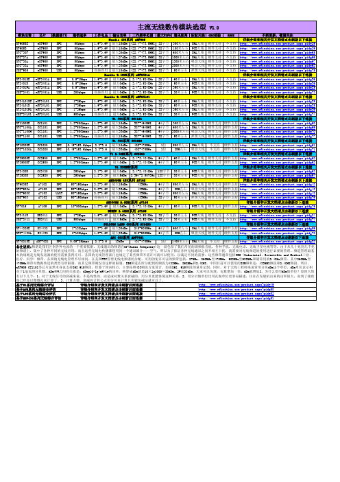
模块名称芯片数据接口通信速率工作电压输出功率工作频率范围最大FIFO 通讯距离标配天线CRC校验RSSI 不断更新,敬请关注详细介绍和相关开发文档请点击刷新以下连接RF905SE nRF905SPI 50kbps 1.9-3.6V 最大10dBm 422.4-473.5MHZ 32字节300米左右SMA天线硬件支持不支持/product.aspx?pid=29RF905B nRF905SPI 50kbps 1.9-3.6V 最大10dBm 422.4-473.5MHZ 32字节100米左右PCB天线硬件支持不支持/product.aspx?pid=29RFC-30F nRF905SPI 50kbps 1.9-3.6V 最大20dBm 422.4-473.5MHZ 32字节600米左右SMA天线硬件支持不支持/product.aspx?pid=65RFC-27A nRF905SPI 50kbps 1.9-3.6V 最大27dBm 422.4-473.5MHZ 32字节1000米左右SMA天线硬件支持不支持/product.aspx?pid=66RFC-30A nRF905SPI 50kbps 1.9-3.6V 最大30dBm 422.4-473.5MHZ 32字节1300米左右吸盘天线硬件支持不支持/product.aspx?pid=67RFC-33A nRF905SPI 50kbps 1.9-3.6V 最大33dBm 422.4-473.5MHZ 32字节2000米左右吸盘天线硬件支持不支持/product.aspx?pid=68USB-905nRF905USB 50kbps 即插即用最大10dBm 422.4-473.5MHZ 32字节50米左右弹簧天线硬件支持不支持/product.aspx?pid=75详细介绍和相关开发文档请点击刷新以下连接RF2401SE nRF2401A SPI 0.5-1Mbps 1.9-3.6V 最大0dBm 2.4-2.524GHz 28字节60米左右SMA天线硬件支持不支持/product.aspx?pid=36RF2401B nRF2401A SPI 0.5-1Mbps 1.9-3.6V 最大0dBm 2.4-2.524GHz 28字节50米左右PCB天线硬件支持不支持/product.aspx?pid=36RF2401PA nRF2401A SPI 0.5-1Mbps 1.9-3.6V 最大0dBm 2.4-2.524GHz 28字节350米左右SMA天线硬件支持不支持/product.aspx?pid=85USB-2401nRF2401A USB 200kbps 即插即用最大0dBm 2.4-2.524GHz 28字节20米左右PCB天线硬件支持不支持/product.aspx?pid=73详细介绍和相关开发文档请点击刷新以下连接RF24L01SE nRF24L01SPI 1-2Mbps 1.9-3.6V 最大0dBm 2.4-2.524GHz 32字节60米左右SMA天线硬件支持不支持/product.aspx?pid=35RF24L01B nRF24L01SPI 1-2Mbps 1.9-3.6V 最大0dBm 2.4-2.524GHz 32字节50米左右PCB天线硬件支持不支持/product.aspx?pid=35RF24L01PA nRF24L01SPI 1-2Mbps 1.9-3.6V 最大0dBm 2.4-2.524GHz 32字节350米左右SMA天线硬件支持不支持/product.aspx?pid=86USB-24L01nRF24L01USB 500kbps 即插即用最大0dBm 2.4-2.524GHz 32字节20米左右PCB天线硬件支持不支持/product.aspx?pid=74详细介绍和相关开发文档请点击刷新以下连接RF1100SE CC1101SPI 1.2-500kbps 1.8-3.6V 最大10dBm 387-464MHZ 64字节300米左右SMA天线硬件支持硬件支持/product.aspx?pid=60RFC-1100A CC1101SPI 1.2-500kbps 1.8-3.6V 最大20dBm 387-464MHZ 64字节600米左右SMA天线硬件支持硬件支持/product.aspx?pid=69RFC-1100H CC1101SPI 1.2-500kbps 1.8-3.6V 最大33dBm 387-464MHZ 64字节2000米左右吸盘天线硬件支持硬件支持/product.aspx?pid=70USB-1100CC1101USB 1.2-500kbps 即插即用最大10dBm 387-464MHZ 32字节50米左右弹簧天线硬件支持硬件支持/product.aspx?pid=77详细介绍和相关开发文档请点击刷新以下连接RF1020SE CC1020SPI 0.45-153.6kbps 2.3-3.6最大10dBm 402-470MHz 1位500米左右SMA天线不支持硬件支持/product.aspx?pid=61RFC-1020A CC1020SPI 0.45-153.6kbps 2.3-3.6最大33dBm 402-470MHz 1位2KM左右吸盘天线不支持硬件支持/product.aspx?pid=71详细介绍和相关开发文档请点击刷新以下连接RF2500SE CC2500SPI 1.2-500kbps 1.8-3.6V 最大0dBm 2.4-2.484GHz 64字节60米左右SMA天线硬件支持硬件支持/product.aspx?pid=62RF2500BF CC2500SPI 1.2-500kbps 1.8-3.6V 最大0dBm 2.4-2.484GHz 64字节50米左右PCB天线硬件支持硬件支持/product.aspx?pid=62详细介绍和相关开发文档请点击刷新以下连接RF2420B CC2420SPI 250kbps 2.1-3.6V 最大0dBm 2.4-2.484GHz 128字节80米左右PCB天线硬件支持硬件支持/product.aspx?pid=63RF2520B CC2520SPI 250kbps 1.8-3.8V 最大5dBm 2.394-2.507GHz 128字节80米左右PCB天线硬件支持硬件支持/product.aspx?pid=64详细介绍和相关开发文档请点击刷新以下连接RF903SE A7102SPI 50-150kbps 2.2-3.6V 最大15dBm 433MHz 64字节500米左右SMA天线硬件支持硬件支持/product.aspx?pid=48RFC-903A A7102SPI 50-150kbps 2.2-3.6V 最大33dBm 433MHz 64字节2KM左右吸盘天线硬件支持硬件支持/product.aspx?pid=48UTC-903C A7102UART 50-150kbps 2.2-3.6V 最大15dBm 433MHz 64字节500米左右SMA天线硬件支持硬件支持/product.aspx?pid=48USB-903A7102USB 50-150kbps 即插即用最大15dBm 433MHz 32字节50米左右弹簧天线硬件支持硬件支持/product.aspx?pid=76详细介绍和开发文档请点击刷新以下连接RF7015A7105SPI 10-500kbps 1.8-3.6V 最大0dBm 2.4-2.484GHz 64字节50米左右PCB天线硬件支持硬件支持/product.aspx?pid=79详细介绍和开发文档请点击刷新以下连接RF2411B BK2411SPI 1-2Mbps 1.9-3.6V 最大5dBm 2.4-2.524GHz 32字节80米左右PCB天线硬件支持不支持/product.aspx?pid=84USB-2411BK2411USB 500kbps 即插即用最大5dBm 2.4-2.524GHz 32字节30米左右PCB天线硬件支持不支持/product.aspx?pid=74详细介绍和开发文档请点击刷新以下连接RF4432SE SI4432SPI 1-128kbps 1.8-3.6V 最大20dBm 240-930MHz 64字节600米左右SMA天线硬件支持硬件支持/product.aspx?pid=59RFC-4432A SI4432SPI 1-128kbps 1.8-3.6V 最大33dBm 240-930MHz 64字节2KM左右吸盘天线硬件支持硬件支持/product.aspx?pid=72详细介绍和开发文档请点击刷新以下连接RF7021SE ADF7021SPI 0.05-25kbps 2.3-3.613dBm 431-470MHz 1位1400米左右SMA天线不支持硬件支持/product.aspx?pid=32 主流无线数传模块选型 V1.0备注说明:频谱是我们区别各种电波的一个重要依据,无线通讯的频谱在RF(Radio Frequency)这一段包括了我们常见的调频收音机,各种手机,无线电话,无线卫星电视等等,由于从几十兆到几千兆的频谱上,集中了各种不同的无线应用,而且这些无线电传播都使用同一个通讯媒介——空气,所以为了保证各种无线通讯之间不相互干扰,就需要对无线频道的使用进行必要的管理。

班级040831学号04083104本科毕业设计(论文)外文资料翻译毕业设计题目大功率对讲机接收电路的设计外文资料题目ADF4110系列芯片数据手册学院机电工程学院专业自动化学生姓名庄伟源指导教师姓名李西安ADF4110系列芯片手册 1RF PLL频率合成器ADF4110、ADF4111、ADF4112、ADF4112特征ADF4110: 550 MHzADF4111: 1.2 GHzADF4112: 3.0 GHzADF4113: 4.0 GHz2.7 V到5.5 V电源独立的电荷泵电源(VP)允许扩展调谐电压,3 V系统可编程双模分频器8/9, 16/17,32/33, 64/65可编程电荷泵电流可编程Antibacklash脉宽3-Wire串行接口模拟和数字锁定检测硬件和软件关断模式应用无线电台(GSM, PCS, DCS,基站CDMA,的WCDMA)无线手机(GSM, PCS, DCS, CDMA,的WCDMA)无线LANS通信测试设备CATV设备概述该频率合成器可用于ADF4110 系列实施的上变频和下本振,无线接收器和发射器变频部分.他们由一个低噪声数字PFD(相位频率检测器),一个精密电荷泵,一个可编程参考分频器,可编程A和B计数器和一个双模预置分频器性(P / P+1).在A (6-bit)和B (13-bit)柜台,联与双模分频器性(P / P+1),实现一N 分(N = BP + A).此外,14-bit引用计数器(R柜),允许在PFD将REFIN频率可选输入.如果使用合成器与外部环路滤波器和VCO(压控振荡器)可以实现一个完整的PLL(锁相环)。
所有片内寄存器的控制是通过一个简单的3-wire接口。
该器件采用功率范围从2.7 V供应5.5 V和断电时,可在不使用.功能框图对应部分翻译:14-bit R counter 14位R计数器;REFERENCE 基准;PHASE FREQUENCY DETECTOR 鉴频鉴相器;CHARGE PUMP 充电泵;R COUNTER LATCH R计数器锁存;24-BIT INPUT REGISTER 24位输入寄存器;FUNCTION LATCH 功能锁存;A, B COUNTER LATCH A、B计数器锁存;LOCK DETECT 锁定检测;CURRENT SETTING 1 电流设置1;CURRENT SETTING 2 电流设置2;ADF4110系列芯片手册2FROM FUNCTION LATCH 来自功能锁存; PRESCALER P/P +1 前置分频器P/P+1; 13-BIT B COUNTER 13位B 计数器;REV:由ADI 公司提供的信息被认为是准确和可靠.但是,没有承担责任的模拟装置 使用,也没有侵犯任何专利或其它第三方权利这可能是由于它的使用.没有获发牌照以暗示或否则根据ADI 公司的任何专利或专利的权利.其中技术的方式,P.O.盒9106,诺伍德,MA 02062-9106, U.S.A. 电话:781/329-4700万维网网址: 传真:781/326-8703 ©模拟装置,Inc., 2000ADF4110系列芯片手册 3ADF4110/ADF4111/ADF4112/ADF4113——规格(AVDD = DVDD = 3 V 10%, 5 V 10%; AVDD ≤ VP ≤ 6.0 V; AGND = DGND = CPGND = 0 V; RSET = 4.7 k ; TA = TMIN to TMAX 除非额外注释)参数B电压B夹单位测试条件/评论RF特征(3 V)RF输入频率ADF4110ADF4110ADF4111ADF4112ADF4112ADF4113RF输入灵敏度最大允许预分频器输出频率33RF特征(5 V)RF输入频率ADF4110ADF4111ADF4112ADF4113ADF4113RF输入灵敏度最大允许预分频器输出频率45/55025/5500.045/1.20.2/3.00.1/3.00.2/3.7–15/016525/5500.025/1.40.1/3.00.2/3.70.2/4.0–10/020045/55025/5500.045/1.20.2/3.00.1/3.00.2/3.7–15/016525/5500.025/1.40.1/3.00.2/3.70.2/4.0–10/0200MHz最小/最大MHz最小/最大GHz最小/最大GHz最小/最大GHz最小/最大GHz最小/最大dBm最小/最大MHz 最大MHz最小/最大GHz最小/最大GHz最小/最大GHz最小/最大GHz最小/最大dBm最小/最大MHz 最大参见图输入电路25.使用低频率的方波输入电平= –10 dBm输入电平= –10 dBm输入电平= –10 dBm使用低频率的方波.输入电平= –5 dBm将REFIN特征将REFIN输入频率参考输入灵敏度4输入电容将REFIN将REFIN输入电流0/100–5/010±1000/100–5/010±100MHz最小/最大dBm最小/最大pF 最大µA最大交流耦合.当直流耦合:0到V DD最大(CMOS兼容)鉴相器鉴相器频率55555MHz 最大电荷泵I CP吸入/源高价值低值绝对精度R SET范围56252.52.7/1056252.52.7/10mA typµAtyp% typkΩ typ可编程:见表V随着R SET= 4.7 kΩ随着R SET= 4.7 kΩ见表VADF4110系列芯片手册4I CP3-State泄漏电流汇和源电流匹配I CP主场迎战V CPI CP与温度的关系121.52121.52nA typ% typ% typ% typ0.5 V≤V CP≤V P– 0.50.5 V≤V CP≤V P– 0.5V CP= V P/2逻辑输入V INH,输入高电压V INL,输入低电压I INH/I INL,输入电流C IN,输入电容0.8×DV DD0.2×DV DD±1100.8×DV DD0.2×DV DD±110V 最小V 最大µA最大pF 最大逻辑输出V OH,输出高电压V OL,输出低电压DV DD– 0.40.4DV DD– 0.40.4V 最小V 最大I OH= 500µAI OL= 500µA电力用品AV DDDV DDV PI DD6(AI DD+ DI DD) ADF4110ADF4111ADF4112ADF4113I P低功耗的睡眠模式2.7/5.5AV DDAV DD/6.05.55.57.5110.512.7/5.5AV DDAV DD/6.05.55.57.5110.51V分钟/视频最大V分钟/视频最大mA 最大mA 最大mA 最大mA 最大mA 最大µAtypAV DD≤V P≤6.0 V见图22和234.5 mA典型4.5 mA典型6.5 mA典型8.5 mA典型T A= 25°C噪声特性ADF4113相位噪声楼7相位噪声性能8ADF4110: 540 MHz输出9 ADF4111: 900 MHz输出10 ADF4112: 900 MHz输出10 ADF4113: 900 MHz输出10 ADF4111: 836 MHz输出11 ADF4112: 1750 MHz输出12 ADF4112: 1750 MHz输出13 ADF4112: 1960 MHz输出14 ADF4113: 1960 MHz输出14 ADF4113: 3100 MHz输出15杂散信号–171–164–91–87–90–91–78–86–66–84–85–86–171–164–91–87–90–91–78–86–66–84–85–86dBc/Hz typdBc/Hz typdBc/Hz typdBc/Hz typdBc/Hz typdBc/Hz typdBc/Hz typdBc/Hz typdBc/Hz typdBc/Hz typdBc/Hz typdBc/Hz typ@ 25千赫频率PFD@ 200千赫频率PFD@ VCO输出@ 1 kHz偏移和200千赫频率PFD@ 1 kHz偏移和200千赫频率PFD@ 1 kHz偏移和200千赫频率PFD@ 1 kHz偏移和200千赫频率PFD@ 300 Hz失调和30千赫频率PFD@ 1 kHz偏移和200千赫频率PFD@ 200 Hz失调和10千赫频率PFD@ 1 kHz偏移和200千赫频率PFD@ 1 kHz偏移和200千赫频率PFD@ 1 kHz偏移频率和1 MHz PFDADF4110系列芯片手册 5ADF4110: 540 MHz输出9 ADF4111: 900 MHz输出10 ADF4112: 900 MHz输出10 ADF4113: 900 MHz输出10 ADF4111: 836 MHz输出11 ADF4112: 1750 MHz输出12 ADF4112: 1750 MHz输出13 ADF4112: 1960 MHz输出14 ADF4113: 1960 MHz输出14 ADF4113: 3100 MHz输出15–97/–106–98/–110–91/–100–100/–110–81/–84–88/–90–65/–73–80/–84–80/–84–80/–82–97/–106–98/–110–91/–100–100/–110–81/–84–88/–90–65/–73–80/–84–80/–84–80/–82dBc typdBc typdBc typdBc typdBc typdBc typdBc typdBc typdBc typdBc typ@ 200千赫/ 400 kHz和200千赫频率PFD@ 200千赫/ 400 kHz和200千赫频率PFD@ 200千赫/ 400 kHz和200千赫频率PFD@ 200千赫/ 400 kHz和200千赫频率PFD@ 30千赫/ 60 kHz和30千赫频率PFD@ 200千赫/ 400 kHz和200千赫频率PFD@ 10千赫/ 20 kHz和10千赫频率PFD@ 200千赫/ 400 kHz和200千赫频率PFD@ 200千赫/ 400 kHz和200千赫频率PFD@ 1 MHz/2 MHz和1 MHz PFD频率附注:1工作温度范围为如下:B版:-40°C至+85°C。
AD421常见问题解答编写人CAST(R)版本号Rev 1.0------------------------------------------------------------------------------------------------------------ 本报告为Analog Devices Inc. (ADI) 中国技术支持中心专用,ADI可以随时修改本报告而不用通知任何使用本报告的人员。
如有任何问题请与china.support@ 联系。
------------------------------------------------------------------------------------------------------------目录1 AD421产品简介 (1)1.1 产品概述 (1)1.2 基本结构及原理 (1)2 AD421 常见问题 (2)2.1 电流环路的电源是不是必须和系统的供电电源分开。
(2)2.2 数据手册中提供的FET管很难买到,有没有其他的能替代呢。
(3)2.3 我该如何通过单片机来控制AD421的编程 (4)2.4 为什么电流输出和我编程的值不相符。
(5)2.5 如果我想让AD421提供超过20mA的电流,可以么? (6)2.6 当AD421给别的器件供电,为什么环路电流会变得不准? (6)2.7 如何用AD421来构建一个电流源? (7)2.8 FET管脚该如何与AD421连接?。
(7)2.9 ADI公司还推出可以替代AD421或者与其类似的产品么? (8)1- 1 -中国技术支持中心 电话:800-810-1742 传真:800-810-1747 Email :china.support@1 AD421产品简介1.1 产品概述AD421是ADI 公司推出的一种单片高性能数模转换器(DA C) 。
它由电流环路供电,16位数字信号串行输入,4~20 mA 电流输出,完全符合设计智能变送器的工业控制标准信号输出要求,可实现远程智能工业控制。
at32f421例程
AT32F421是Atmel公司推出的一款基于ARM Cortex-M4架构的微控制器。
由于具体的例程会取决于您要实现的具体功能,因此我无法提供完整的AT32F421例程。
然而,我可以为您提供一个简单的AT32F421初始化例程,以便您开始使用该微控制器。
请注意,以下代码仅用于参考,并可能需要根据您的具体需求进行修改:
c
#include "at32f4xx.h"
void SystemClock_Config(void);
void Error_Handler(void);
void GPIO_Init(void);
int main(void)
{
HAL_Init();
SystemClock_Config();
GPIO_Init();
while (1)
{
// 在此处添加您的代码逻辑
}
}
void SystemClock_Config(void)
{
// 此处添加系统时钟配置代码
}
void GPIO_Init(void)
{
// 此处添加GPIO初始化代码
}
void Error_Handler(void)
{
while (1)
{
// 错误处理代码,例如LED闪烁或其他错误指示
}
}
这是一个基本的框架,您可以根据自己的需求添加适当的函数和逻辑。
如果您需要关于特定外设、功能或例程的更详细信息,建议您参考Atmel官方的
AT32F421数据手册和参考手册,或查找相关的开发社区和论坛以获取更多帮助。
Dual Low Power PLL Frequency SynthesizerData SheetADF4212LRev. DInformation furnished by Analog Devices is believed to be accurate and reliable. However , no responsibility is assumed by Analog Devices for its use, nor for any infringements of patents or other rights of third parties that may result from its use. Specifications subject to change without notice. No license is granted by implication or otherwise under any patent or patent rights of Analog Devices. T rademarks and registered trademarks are the property of their respective owners.One Technology Way, P.O. Box 9106, N orwood, MA 02062-9106, U.S.A. Tel: 781.329.4700 Fax: 781.461.3113 ©2002–2012 Analog Devices, Inc. All rights reserved.FEATURESI DD total: 7.5 mABandwidth RF/IF: 2.4 GHz/1.0 GHz 2.7 V to 3.3 V power supplySeparate V P allows extended tuning voltage Programmable dual modulus prescaler RF and IF: 8/9, 16/17, 32/33, 64/65 Programmable charge pump currents 3-wire serial interfaceAnalog and digital lock detect Fastlock mode Power-down mode20-lead TSSOP and 20-lead LFCSP packagesAPPLICATIONSWireless handsets (GSM, PCS, DCS, DSC1800, CDMA, WCDMA)Base stations for wireless Radio (GSM, PCS, DCS, CDMA, WCDMA) Wireless LANSCable TV tuners (CATV)Communications test equipmentGENERAL DESCRIPTIONThe ADF4212L is a dual frequency synthesizer that can be used to implement local oscillators (LO) in the up-conversion and down-conversion sections of wireless receivers and transmitters. It can provide the LO for both the RF and IF sections. It consists of a low noise digital phase frequency detector (PFD), a precision charge pump, a programmable reference divider, programmable A and B counters, and a dual modulus prescaler (P/P + 1). The A (6-bit) and B (12-bit) counters, in conjunction with the dual modulus prescaler (P/P + 1), implement an N divider (N = BP + A). In addition, the 15-bit reference counter (R counter) allows selectable REF IN frequencies at the PFD input. A complete phase-locked loop (PLL) can be implemented if the synthesizer is used with external loop filters and voltage controlled oscillators (VCOs). Control of all the on-chip registers is via a simple 3-wire interface with 1.8 V compatibility. The devices operate with a power supply ranging from 2.7 V to 3.3 V and can be powered down when not in use.FUNCTIONAL BLOCK DIAGRAMRF INRFRFIFIFOREF IF IN02774-001IFRFFigure 1.ADF4212LData SheetRev. D | Page 2 of 28TABLE OF CONTENTSFeatures .............................................................................................. 1 Applications ....................................................................................... 1 General Description ......................................................................... 1 Functional Block Diagram .............................................................. 1 Revision History ............................................................................... 2 Specifications ..................................................................................... 3 Timing Characteristics ................................................................ 5 Absolute Maximum Ratings ............................................................ 6 ESD Caution .................................................................................. 6 Pin Configurations and Function Descriptions ........................... 7 Typical Performance Characteristics ............................................. 9 Circuit Description ......................................................................... 13 Reference Input Section ............................................................. 13 RF/IF Input Stage........................................................................ 13 Prescaler (P/P + 1) ...................................................................... 13 RF/IF A and B Counters ............................................................ 13 Pulse Swallow Function ............................................................. 13 RF/IF R Counter ......................................................................... 13 Phase Frequency Detector (PFD) and Charge Pump ............ 14 MUXOUT and Lock Detect ...................................................... 14 Lock Detect ................................................................................. 14 RF/IF Input Shift Register ......................................................... 14 IF R Counter Latch..................................................................... 16 IF N Counter Latch .................................................................... 17 RF R Counter Latch ................................................................... 18 RF N Counter Latch ................................................................... 19 Program Modes .............................................................................. 20 IF and RF Power-Down ............................................................. 20 IF Section ..................................................................................... 20 RF Section ................................................................................... 21 Applications Information .............................................................. 22 Local Oscillator for GSM Handset Receiver ............................... 22 Wideband PLL ............................................................................ 23 Interfacing ................................................................................... 24 PCB Design Guidelines for Lead FrameChip Scale Package ..................................................................... 24 Outline Dimensions ....................................................................... 25 Ordering Guide .. (26)REVISION HISTORY8/12—Rev. C to Rev DChanged CP-20-1 to CP-20-6 ........................................... U niversal Updated Outline Dimensions ....................................................... 25 Changes to Ordering Guide . (26)11/10—Rev. B to Rev CChanges to V P 1, V P 2 to GND Parameter, Table 4 and V P 1, V P 2 to V DD 1, V DD 2 Parameter, Table 4 ................................................... 6 Changes to Ordering Guide . (26)9/08—Rev. A to Rev BUpdated Format .................................................................. U niversal Changes to Figure 1 and General Description Section ............... 1 Changes to Prescaler Output Frequency Parameter and RFInput Frequency (RF IN ) Parameter ................................................. 3 Changes to Table 3 and Figure 2 ..................................................... 5 Changes to Figure 4 .......................................................................... 7 Changes to Figure 27, RF/IF A and B Counters Section, Pulse Swallow Function Section, and RF/IF R Counter Section ........ 13 Changes to RF/IF Input Shift Register Section ........................... 14 Changes to Programmable IF Reference (R) Counter Section, IF Program Modes Section, and IF Power-Down Section ........ 20 Changes to Programmable RF Reference (R) Counter Section, RF Program Modes Section, Programmable RF N Counter Section, and RF Power-Down Section ......................................... 21 Changes to Figure 32 ...................................................................... 23 Changes to Figure 33 and Figure 34 ............................................ 24 Added PCB Design Guidelines for Lead Frame Chip ScalePackage Section............................................................................... 24 Updated Outline Dimensions ....................................................... 25 Changes to Ordering Guide . (25)3/03—Data Sheet changed from REV . 0 to REV . AChanges to General Description ..................................................... 1 Changes to Specifications ................................................................. 3 Changes to Table 9 .......................................................................... 18 Changes to Table 11 ....................................................................... 20 Changes to Figure 31 . (23)11/02—Revision 0: Initial VersionData SheetADF4212LRev. D | Page 3 of 28SPECIFICATIONSV DD 1 = V DD 2 = 2.7 V to 3.3 V; V P 1, V P 2 = V DD to 5.5 V; AGND RF = DGND RF = AGND IF = DGND IF = 0 V; T A = T MIN to T MAX , unless otherwise noted; dBm referred to 50 Ω. Table 1.Parameter 1B Version B Chips 2 Unit Test Conditions/Comments RF/IF CHARACTERISTICSRF Input Frequency (RF IN ) 0.2/2.4 0.2/2.4 GHz min/max For lower frequencies, ensure that slew rate (SR) > 140 V/µs RF Input Sensitivity −10/0 −10/0 dBm min/max V DD = 3 V IF Input Frequency (IF IN ) 100/1000 100/1000 MHz min/maxIF Input Sensitivity −10/0 −10/0 dBm min/max V DD = 3 V MAXIMUM ALLOWABLEPrescaler Output Frequency 3 188 188 MHz maxREF IN CHARACTERISTICSSee Figure 26 for input circuit REF IN Input Frequency 10/150 10/150 MHz min/maxREF IN Input Sensitivity 500 mV/V DD 500 mV/V DD V p-p min/max AC-coupled; when dc-coupled, 0 V to V DD maximum (CMOS compatible) REF IN Input Capacitance 10 10 pF max REF IN Input Current ±100 ±100 μA max PHASE DETECTORPhase Detector Frequency 4 75 75 MHz max CHARGE PUMPI CP Sink/SourceProgrammable, see Table 10 High Value 5 5 mA typ With R SET = 2.7 kΩ Low Value625 625 μA typAbsolute Accuracy 22% typWith R SET = 2.7 kΩ R SET Range1.5/5.6 1.5/5.6 kΩ min/max I CP Three-State Leakage Current 1 1 nA maxSink and Source Current Matching 6 6 % typ 0.5 V < V CP < V P − 0.5 V I CP vs. V CP2 2 % typ 0.5 V < V CP < V P − 0.5 V I CP vs. Temperature 2 2 % typ V CP = V P /2 LOGIC INPUTSV INH , Input High Voltage 1.4 1.4 V min V INL , Input Low Voltage 0.6 0.6 V max I INH /I INL , Input Current ±1 ±1 μA max C IN , Input Capacitance 10 10 pF max LOGIC OUTPUTSV OH , Output High Voltage 1.4 1.4 V min Open-drain 1 kΩ pull-up to 1.8 V V OL , Output Low Voltage 0.4 0.4 V max I OL = 500 μA POWER SUPPLIESV DD 1 2.7/3.3 2.7/3.3 V min/max V DD 2 V DD 1 V DD 1 V min/max V P 1, V P 2 V DD 1/5.5 V DD 1/5.5 V min/max I DD (RF and IF)5 7.5/10 7.5/10 mA typ/max RF Only 5.0/6 5.0/6 mA typ/max IF Only 2.5/4 2.5/4 mA typ/max I P (I P 1 + I P 2)0.6 0.6 mA typ Low Power Sleep Mode11μA typ1 Operating temperature range is as follows: B version: −40°C to +85°C. 2The B chip specifications are given as typical values. 3This is the maximum operating frequency of the CMOS counters. The prescaler value should be chosen to ensure that the RF input is divided down to a frequency less than this value. 4Guaranteed by design. Sample tested to ensure compliance. 5T A = 25°C. RF = 1 GHz; prescaler = 32/33. IF = 500 MHz; prescaler = 16/17.ADF4212LData SheetRev. D | Page 4 of 28V DD 1 = V DD 2 = 2.7 V to 3.3 V; V P 1, V P 2 = V DD to 5.5 V; AGND RF = DGND RF = AGND IF = DGND IF = 0 V; T A = T MIN to T MAX , unless otherwise noted; dBm referred to 50 V . Table 2.Parameter 1B Version B Chips 2 Unit Test Conditions/Comments NOISE CHARACTERISTICSRF Phase Noise Floor 3 −170 −170 dBc/Hz typ 25 kHz PFD frequency−162 −162 dBc/Hz typ 200 kHz PFD frequency Phase Noise Performance 4VCO outputIF: 540 MHz Output 5 −89 −89 dBc/Hz typ 1 kHz offset and 200 kHz PFD frequency IF: 900 MHz Output 6 −87 −87 dBc/Hz typ 1 kHz offset and 200 kHz PFD frequency RF: 900 MHz Output 6 −89 −89 dBc/Hz typ 1 kHz offset and 200 kHz PFD frequency RF: 1750 MHz Output 7 −84 −84 dBc/Hz typ 1 kHz offset and 200 kHz PFD frequency RF: 2400 MHz Output 8 −87 −87 dBc/Hz typ 1 kHz Offset and 1 MHz PFD frequency Spurious SignalsIF: 540 MHz Output 5 −88/−90 −88/−90 dB typ 200 kHz/400 kHz and 200 kHz PFD frequency IF: 900 MHz Output 6 −90/−94 −90/−94 dB typ 200 kHz/400 kHz and 200 kHz PFD frequency RF: 900 MHz Output 6 −90/−94 −90/−94 dB typ 200 kHz/400 kHz and 200 kHz PFD frequency RF: 1750 MHz Output 7 −80/−82 −80/−82 dB typ 200 kHz/400 kHz and 200 kHz PFD frequency RF: 2400 MHz Output 8−80/−82 −80/−82 dB typ 200 kHz/400 kHz and 200 kHz PFD frequency1 Operating temperature range is as follows: B version: −40°C to +85°C. 2The B Chip specifications are given as typical values. 3The synthesizer phase noise floor is estimated by measuring the in-band phase noise at the output of the VCO and subtracting 20logN (where N is the N divider value). See Figure 9. 4The phase noise is measured with the EVAL-ADF4212EB and the HP8562E spectrum analyzer. The spectrum analyzer provides the REFIN for the synthesizer (f REFOUT = 10 MHz @ 0 dBm). 5f REFIN = 10 MHz; f PFD = 200 kHz; offset frequency = 1 kHz; f IF = 540 MHz; N = 2700; loop B/W = 20 kHz 6f REFIN = 10 MHz; f PFD = 200 kHz; offset frequency = 1 kHz; f RF = 900 MHz; N = 4500; loop B/W = 20 kHz 7f REFIN = 10 MHz; f PFD = 200 kHz; offset frequency = 1 kHz; f RF = 1750 MHz; N = 8750; loop B/W = 20 kHz 8f REFIN = 10 MHz; f PFD = 1 MHz; offset frequency = 1 kHz; f RF = 2400 MHz; N = 9800; loop B/W = 20 kHzData SheetADF4212LRev. D | Page 5 of 28TIMING CHARACTERISTICSV DD 1 = V DD 2 = 2.6 V to 3.3 V; V P 1, V P 2 = V DD to 5.5 V; AGND RF = DGND RF = AGND IF = DGND IF = 0 V; T A = T MIN to T MAX , unless otherwise noted; dBm referred to 50 Ω. Table 3.Parameter 1 Limit at T MIN to T MAX (B Version) Unit Test Conditions/Comments t 1 20 ns min LE setup timet 2 10 ns min Data to clock setup time t 3 10 ns min Data to clock hold time t 4 25 ns min Clock high duration t 5 25 ns min Clock low duration t 6 10 ns min Clock to LE setup time t 720 ns minLE pulse width1Guaranteed by design but not production tested.CLKDATALELEFigure 2. Timing DiagramADF4212LData SheetRev. D | Page 6 of 28ABSOLUTE MAXIMUM RATINGST A = 25°C, unless otherwise noted.Table 4. Parameter 1, 2 Ra t ing V DD 1 to GND −0.3 V to +3.6 V V DD 1 to V DD 2 −0.3 V to +0.3 V V P 1, V P 2 to GND −0.3 V to +5.8 V V P 1, V P 2 to V DD 1, V DD 2−0.3 V to +5.8 VDigital I/O Voltage to GND −0.3 V to DV DD + 0.3 V Analog I/O Voltage to GND −0.3 V to V DD + 0.3 V REF IN , RF IN , IF IN to GND−0.3 V to V DD + 0.3 V Operating Temperature RangeIndustrial (B Version)−40°C to +85°C Storage Temperature Range −65°C to +150°C Maximum Junction Temperature 150°C TSSOP θJA Thermal Impedance 150.4°C/W LFCSP θJA Thermal Impedance (Paddle Soldered)122°C/W LFCSP θJA Thermal Impedance (Paddle Not Soldered) 216°C/W Lead Temperature, SolderingVapor Phase (60 sec) 215°C Infrared (15 sec)220°C1This device is a high performance RF integrated circuit with an ESD rating of <2 kV, and is ESD sensitive. Proper precautions should be taken for handling and assembly. 2GND = AGND = DGND = 0 V.Stresses above those listed under Absolute Maximum Ratings may cause permanent damage to the device. This is a stressrating only; functional operation of the device at these or any other conditions above those indicated in the operational section of this specification is not implied. Exposure to absolute maximum rating conditions for extended periods may affect device reliability.ESD CAUTIONData SheetADF4212LRev. D | Page 7 of 28PIN CONFIGURATIONS AND FUNCTION DESCRIPTIONSV P 1CP RF DGND RFFL O AGND RFRF IN V DD 1MUXOUT DGND IFREF IN V P 2CP IFDGND IF R SET AGND IF IF INCLKDATA LE V DD 202774-003Figure 3. TSSOP Pin Configuration CP RF DGND RFRF IN AGND RFFL ONOTES1. IT IS RECOMMENDED THAT THE EXPOSED PADBE THERMALLY CONNECTED TO A COPPER PLANE FOR ENHANCED THERMAL PERFORMANCE. THE PAD SHOULD BE GROUNDED AS WELL.AGND IF IF INDGND IF RSET LER E F I N D G N D I F M U X O U T D A T A C L K V D D 2V D D 1V P 1V P 2C P I F 02774-00414131215117689101920181716Figure 4. LFCSP Pin ConfigurationADF4212LData SheetRev. D | Page 8 of 28Pin No.Mnemonic TSSOP LFCSP DescriptionV DD 2 20 18 Power Supply for the IF, Digital, and Interface Section. Decoupling capacitors to the ground plane should be placed as close as possible to this pin. V DD 2 should have a value of between 2.6 V and 3.3 V. V DD 2 must have the same potential as V DD 1.V DD 1 1 19 Power Supply for the RF Section. Decoupling capacitors to the ground plane should be placed as closeas possible to this pin. V DD 1 should have a value of between 2.6 V and 3.3 V. V DD 1 must have the same potential as V DD 2.V P 1 2 20 Power Supply for the RF Charge Pump. This should be greater than or equal to V DD 1. In systems whereV DD 1 is 3 V, it can be set to 5.5 V and used to drive a VCO with a tuning range up to 5.5 V.EPExposed Pad It is recommended that the exposed pad be thermally connected to a copper plane for enhanced thermal performance. The pad should be grounded as well.Data SheetADF4212LRev. D | Page 9 of 28TYPICAL PERFORMANCE CHARACTERISTICSA M P L I T U D E (dB m )–5–10–15–20–25–300500100015002000FREQUENCY (MHz)2500300002774-005Figure 5. Input Sensitivity (RF Input) A M P L I T U D E(d B m )FREQUENCY (MHz)02774-006Figure 6. Input Sensitivity (IF Input)O U T P U T P O W E R (d B )0–10–20–30–40–50–60–70–80–90–100FREQUENCY (Hz)02774-007Figure 7. Phase Noise, RF Side (1750 MHz, 200 kHz, 20 kHz)02774-0O U T P U T P O W E R (d B )–100–400k –200k 1.75G 200k 400kFREQUENCY (Hz)Figure 8. Reference Spurs, RF Side (1750 MHz, 200 kHz, 20 kHz)P H A S E N O I S E (d B c /H z )–50–60–70–80–90–100–110–120–130–140–150100HzFREQUENCY OFFSET FROM 1.75GHz CARRIER10dB/DIV RMS NOISE = 1.38 DEGREESR L = –50dBc/Hz1MHz02774-009Figure 9. Integrated Phase Noise (1750 MHz, 200 kHz/20 kHz)O U T P U T P O W E R (d B )–10–20–30–40–50–60–70–80–90–100–2k–1k540M1k2kFREQUENCY (Hz)02774-01Figure 10. Phase Noise, IF Side (540 MHz, 200 kHz/20 kHz)ADF4212LData SheetRev. D | Page 10 of 28O U T P U T P O W E R (d B )0–10–20–30–40–50–60–70–80–90–100–400k –200k540M200k 400kFREQUENCY (Hz)02774-011Figure 11. Reference Spurs, IF Side (540 MHz, 200 kHz, 20 kHz)P H A S E N O I S E (d B c /Hz )–50–60–70–80–90–100–110–120–130–140–150100Hz1MHzFREQUENCY OFFSET FROM 540MHz CARRIER10dB/DIV RMS NOISE =0.83 DEGREESR L = –50dBc/Hz02774-012Figure 12. Integrated Phase Noise (540 MHz, 200 kHz/20 kHz)PHASE DETECTOR FREQUENCY (kHz)1010kP H A S E N O I S E (d B c /H z )1k100–130–140–150–160–170–18002774-013Figure 13. Phase Noise Referred to CP Output vs. PFD Frequency, RF SidePHASE DETECTOR FREQUENCY (kHz)1010kP H A S EN O I S E (d B c /H z )1k100–130–140–150–160–170–18002774-014Figure 14. Phase Noise Referred to CP Output vs. PFD Frequency, IF SideV CP (V)0I C P(m A )1642–2–42345–602774-015Figure 15. RF Charge Pump Output CharacteristicsV CP (V)0I C P (m A )1642–2–42345–6V DD =3V V P 2=5.5V02774-016Figure 16. IF Charge Pump Output Characteristics分销商库存信息:ANALOG-DEVICESADF4212LBCPZ-RL ADF4212LBRUZ-RL ADF4212LBCPZ-RL7 ADF4212LBRUZ-RL7ADF4212LBCPZ ADF4212LBRUZ。