厚声电阻 rohs CTI
- 格式:pdf
- 大小:2.12 MB
- 文档页数:7

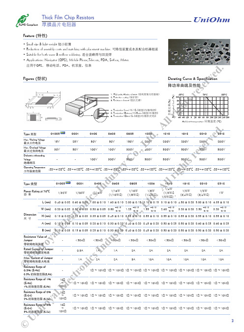
ContentsIntroduction ………………………………………………………………………………………Page1.0 Scope (4)2.0 Ratings & Dimension ………………………………………………………….…………....4~53.0 Structure.................................... (5)4.0 Marking…….…………………………………… ………………………. ..… …………… 6~75.0 Derating Curve................................................... .. (8)6.0 Performance Specification …………………………………………….……………..........8~97.0 Explanation of Part No. System ………………………………….…………………………9~108.0 Ordering Procedure (10)9.0 Standard Packing ………………………………………………….…………………………11~1210.0 Note Matter.................................................................. . (12)File Name:CHIP SERIES±0.5%,±1%,±2%,±5%& 0ΩDate 2013.12.20EditionNo. 1Amendment Record Signature Edition Prescription of amendment Amend Page Amend Date Amended by Checked by1.0 Scope:This specification for approve relates to the Lead-Free Thick Film Chip Resistors manufactured byROYALOHM.2.0 Ratings & Dimension:01005、0201、04020603、0805、1206、1210、1812、2010、25122.1 Dimension & Resistance Range :Type70℃ PowerDimension(mm) Resistance RangeL W H A B 0.5% 1.0% 2.0% 5.0%01005 1/32W 0.40±0.02 0.20±0.02 0.13±0.02 0.10±0.050.10±0.03--10Ω-10M Ω 10Ω-10M Ω10Ω-10M Ω0201 1/20W 0.60±0.03 0.30±0.03 0.23±0.03 0.10±0.050.15±0.05-- 1Ω-10M Ω 1Ω-10M Ω1Ω-10M Ω0402 1/16W 1.00±0.100.50±0.05 0.35±0.05 0.20±0.100.25±0.101Ω-10M Ω0.2Ω~22M Ω 0.2Ω~22M Ω0.2Ω~22M Ω06031/16W 1/10WS 1.60±0.10 0.80±0.10 0.45±0.10 0.30±0.200.30±0.201Ω-10M Ω0.1Ω~33M Ω 0.1Ω~33M Ω0.1Ω~100M Ω0805 1/10W 1/8WS 2.00±0.15 +0.151.25-0.10 0.55±0.10 0.40±0.200.40±0.201Ω-10M Ω0.1Ω~33M Ω 0.1Ω~33M Ω0.1Ω~100M Ω1206 1/8W 1/4WS 3.10±0.15 +0.151.55-0.100.55±0.10 0.45±0.200.45±0.201Ω-10M Ω0.1Ω~33M Ω 0.1Ω~33M Ω0.1Ω~100M Ω1210 1/4W1/3WS 1/2WSS3.10±0.10 2.60±0.20 0.55±0.10 0.50±0.250.50±0.201Ω-10M Ω0.1Ω~10M Ω 0.1Ω~22M Ω0.1Ω~100M Ω18121/2W 3/4WS 4.50±0.20 3.20±0.20 0.55±0.20 0.50±0.200.50±0.200.1Ω-10M Ω0.1Ω-10M Ω 0.1Ω-10M Ω0.1Ω-10M Ω2010 1/2W 3/4WS5.00±0.10 2.50±0.20 0.55±0.10 0.60±0.250.50±0.201Ω-10M Ω0.1Ω~22M Ω 0.1Ω~22M Ω0.1Ω~22M Ω2512 1W 6.35±0.10 3.20±0.20 0.55±0.10 0.60±0.250.50±0.201Ω-10M Ω0.1Ω~33M Ω 0.1Ω~33M Ω0.1Ω~33M Ω2.2 RatingsType70℃PowerMax 。

Page 4•Small size and lightweight• Suitable for both flow and reflow soldering•Reduction of assembly costs and matching with placement machines2006 - 20072006 - 2007 Page 52006 - 2007Marking on the Resistors Body:• For 0402 size, no marking on the body due to the small size of the resistor.•±5% tolerance product. (Including resistance values less than 1Ω; both 1% and 5%) The marking is 3 digits, the first 2 digits are the significant figures of the resistance and the 3rd digit denotes number of zeros.153 = 15000Ω = 15K Ω; 120 = 12ΩBelow 10Ω shown as this: 6R8 = 6.8Ω• 1% tolerance marking of case size 0805 and bigger is 4 digits, the first 3 digits are the significant figures of the resistance and the 4th digit denotes number of zeros.2372 = 23700Ω = 23.7K Ω; 1430 = 143Ω Below 10Ω shown as this: 3R24 = 3.24ΩPage 6* More details, please see pages 77-78.• Standard E-96 series values (±1% tolerance) of 0603 size. Due to the small size of the resistor’s body, 3 digitsmarking will be used to indicate the accurate resistance value by using the Multiplier code & Standard E-96 Series Resistance Value Code as shown on Page 6.1.96K Ω = 196 x 101 Ω = 29B12.4Ω = 124 x 10-1 Ω = 10X• Standard E-24 series values which does not belong to E-96 series values (±1% tolerance) of 0603 size. The marking is the same as 5% tolerance but mark with underline.122 = 1200 = 1.2K Ω 680 = 68ΩTemperature coefficient ±5%: 1Ω ~ 10M Ω ≤ ±200PPM/°C±1%: 10Ω ~ 100Ω ≤ ±200PPM/°C; 101Ω ~ 1M Ω ≤ ±100PPM/°CShort-time overload ±5%: ±(2.0% + 0.1Ω) Max.±1%: ±(1.0% + 0.1Ω) Max.Insulation resistanceMin. 1,000 Mega OhmDielectric withstanding voltageNo evidence of flashover, mechanical damage, arcing or insulation breakdown Terminal bending±(1.0% + 0.05Ω) Max.Soldering heat ±(1.0% + 0.05Ω) Max.SolderabilityMin. 95% coverage Temperature cycling±5%: ±(1.0% + 0.05Ω) Max.±1%: ±(0.5% + 0.05Ω) Max.Humidity (Steady s tate) ±5%: ±(3.0% + 0.1Ω) Max.±1%: ±(0.5% + 0.1Ω) Max.Load life in humidity±5%: ±(3.0% + 0.1Ω) Max.±1%: ±(1.0% + 0.1Ω) Max.Load life±5%: ±(3.0% + 0.1Ω) Max.±1%: ±(1.0% + 0.1Ω) Max.* The values which are not of standard E-24 series (2% & 5%) and not of E-96 series (1%) could be offered on a case to case basis.2006 - 2007Page 7。

rohs电阻RoHS电阻是符合欧盟限制使用某些有害物质指令(Restriction of Hazardous Substances Directive,简称RoHS)的一种电子元件。
RoHS指令是为了保护环境和人体健康而制定的,规定了电子产品中禁止使用的有害物质。
RoHS电阻是在满足RoHS指令要求的基础上生产的一种电阻元件。
RoHS指令于2003年2月13日正式生效,其目的是限制电子产品中六种有害物质的使用,包括铅(Pb)、汞(Hg)、镉(Cd)、六价铬(Cr6+)、多溴联苯(PBBs)和多溴二苯醚(PBDEs)。
这些物质在电子产品的制造、使用和处理过程中可能对环境和人体健康造成严重危害。
RoHS电阻作为一种被广泛应用于电子产品中的元件,其材料和制造工艺都需要符合RoHS指令的要求。
首先,RoHS电阻的材料中不能含有上述六种有害物质,特别是铅这种常见的元素。
其次,RoHS电阻的制造工艺也需要符合环保要求,避免使用对环境有害的化学物质和工艺。
RoHS电阻在电子产品中起到了非常重要的作用。
电阻作为一种基本的电子元件,用于控制电流、分压、限流等功能,广泛应用于电路板、电源、通信设备、汽车电子等领域。
RoHS电阻的使用不仅满足了电子产品的功能要求,还保护了环境和人体健康,符合可持续发展的理念。
为了确保RoHS电阻的质量和符合性,生产厂家需要进行严格的质量控制和测试。
首先,厂家需要选择符合RoHS指令要求的原材料供应商,确保原材料的质量和符合性。
其次,厂家需要建立完善的质量管理体系,从生产过程中的控制到最终产品的测试,确保RoHS电阻的质量和符合性。
最后,RoHS电阻需要进行相关的检测和认证,通过第三方机构的审核,确保产品的质量和符合性。
RoHS电阻的应用还面临一些挑战和问题。
首先,一些电子产品的设计和制造过程中仍存在对有害物质的需求,这就需要在满足RoHS指令要求的前提下,寻找替代材料和工艺。
其次,RoHS电阻的价格相对传统电阻可能会稍高,这对一些成本敏感的电子产品制造商来说是一个挑战。

Application Note 应用指南Product Name:Chip Resistor产品名称:晶片电阻器Uniroyal Electronics Global Co., Ltd. 厚声国际贸易(昆山) 有限公司Building # 3, No. 88 Longteng Road, Economic & Technical Development Zone, Kunshan City, Jiangsu Province, China 215333 中国江苏省昆山市经济技术开发区龙腾路88号3号房TEL: +86 512 3687 3924Email: **************/CONTENT目录1SAFETY CONSIDERATION安全注意事项 (1)2USAGE CONSIDERATIONS使用注意事项 (2)3MOUNTING CONSIDERATION安装注意事项 (3)4STORAGE CONSIDERATION存储的注意事项 (7)5EXPORTATION CONSIDERATION出口注意事项 (7)6INDUSTRIAL PROPERTY PROHIBITIONS工业产权禁令 (7)7TECHNICAL GUIDANCE技术指导 (8)8OTHER MATTERS其他事项 (16)NOTES说明 (18)1Safety consideration安全注意事项1.1The products are designed and produced for application in ordinary electronic equipment (AV equipment, telecommunication equipment, home appliances amusement, etc.).If the products are to be used in devices requiring extremely high reliability (medical equipment, transport equipment, aircraft/spacecraft, nuclear power controllers, car equipment including car accessories, safety devices, etc.) and whose failure or operational error may endanger human life, please consult with the company,s Sale’s Dept. to advance.产品被设计和生产用于普通电子设备(AV设备、电信设备、家电娱乐等)。
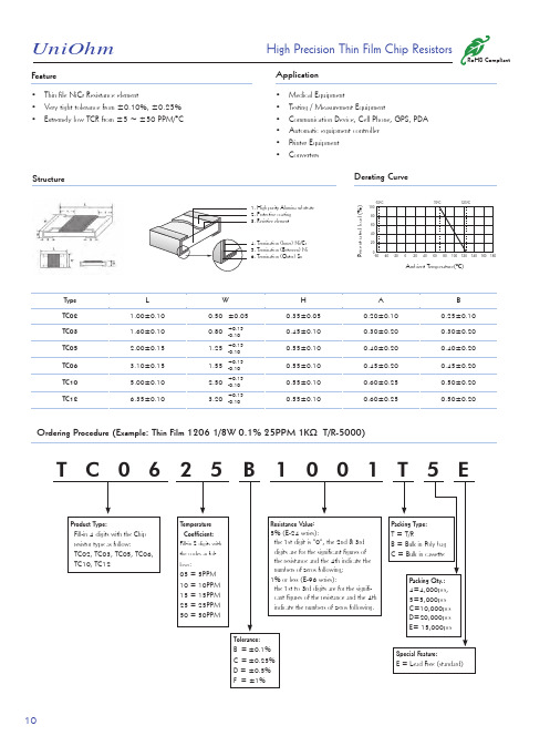
E xplanation of Part No. System1234567891011121314The standard Part No. includes 14 digits with the following explanation: 1. 1st ~4th digits: a) This is to indicate the SMD Resistor size. Example: 1206, TC05 or HV03;b) For Resistor Network & Coated type, the 1st ~3rd digits are to indicate the product type and the 4th digit is the special feature. Example: RNLA = Resistor Newtork Circuit A type; CFRF = Carbon Film Fixed Resistors Non-Flame type; MORI = Metal Oxide Film Fixed Resistor Non-Inductive type.c) For Cement Fixed Resistors, these 4 digits are to indicate the product type but if the product type has only 3 digits, the 4th digit will be "0". Example: PRW0=PRWtype; PRWC=PRWC type.2. 5th ~ 6th digits:a) This is to indicate the wattage or power rating. To distinguish the sizes and the umbers, the following codes are used, and please refer to the following chart for details: W= Normal Size; S = Small Size; U = Ultra Small Size; “1” ~ “G” to denotes “1” ~ “16” as Hexadecimal:b) For power rating less than 1W , the 5th digit will be the letters W , S or U to represent the size required & the 6th digit will be a number or a letter code. Example: WA= 1/10W; U2 = 1/2W-SS.c) For power rating of 1W to 16W , the 5th digit will be a number or a letter code and the 6th digit will be the letters of W , S or U. Example: AW = 10W; 3S =3W-S.d) For power rating between 20W to 99W , the 5th & 6th digits will show the whole numbers of the power rating itself. Example: 20 = 20W; 75 = 75W .e) For power rating of 100W & over, the 5th & 6th digits will be indicated with "00" and the actual wattge being indicated at the last 3 digits (12th ~14th ) of the PartNo.f) For special power ratings, the following codes ar bo be used: 1). WH = 1/32W (10P8 Chip Network) 3). 04 = 0.4W-SS (0.4 watt Ultra Small size)5). 2A = 2.5W2). 07 = 3/4-S (Chip 2010 size)4). 06 = 0.6W-S (0.6 watt Small size) 6). 6A = 6.5Wg) For Resistor Network, since the power rating is fixed as 1/8W for A circuit & 1/5W for B circuit, the 5th & 6th digit is to be used to denote the number of pins required. Example: 09 = 9pins; 12 = 12pins.h) For Jumper Wires the 5th & 6th digits will be indicated with "00".i) For Thin Film Chip Resistors, these 2 digits will be used to indicated the requested Temperature coefficient:1). 05 = 5PPM 2). 10 = 10PPM3). 15 = 15PPM4). 25 = 25PPM5). 50 = 50PPM3. The 7th digit is to denote the Resistance Tolerance. The following letter code is to be used for indicating the standard Resisance Tolerance. As for Metal Film Fixed Resistorproducts, it is also to denote the standard PPM as follows:B = ±0.1% (15PPM) G = ±2% (100PPM)C = ±0.25% (25PPM) J = ±5% (200PPM)D = ±0.5% (50PPM) K = ±10%F = ±1%(50PPM)Remark: if it it not one of the above standard "tolerance-TCR", the requirement should be clearly stated when placing order.Example: ±1% (25PPM), the 7th digit still shows “F” but separately note the requirement of “25PPM”Wattage 1/21/31/41/51/61/71/81/91/101/111/121/131/141/151/16Normal Size W2W3W4W5W6W7W8W9WA WB WC WD WE WF WG Small Size S2S3S4S5S6S7S8S9SA SB SC SD SE SF SG Ultra Small SizeU2U3U4U5U6U7U8U9UAUBUCUDUEUFUGWattage 12345678910111213141516Normal Size lW 2W 3W 4W 5W 6W 7W 8W 9W AW BW CW DW EW FW GW Small Size 1S 2S 3S 4S 5S 6S 7S 8S 9S AS BS CS DS ES FS GS Ultra Small Size1U2U3U4U5U6U7U8U9UAUBUCUDUEUFUGU1/16W ~ 1/2W (<1W)1W ~ 16W (≥1W)UniOhm794. The 8th to 11th digits is to denote the Resistance V alue:a) For the standard resistance values of E-24 series in 5% & 10% tolerance, the 9th digit is "0", the 9th & 10th digits are to denote the significant figuresof the resistance and the 11th digit is the number of zeros following.b) For the standard resistance values of E-96 series in 1% (or less) & 2% tolerance, the 8th digit to the 10th digits are to denote the significant figures ofthe resistance and the 11th digit is the number of zeros following.c) For the code of the significant figures of E-24 & E-96 series, please refer to page 77 & 78 of the standard Resistance Value list.d) The following numbers and the letter codes is to be used to indicate the number of zeros in the 11th digit:0 = 100 1 = 101 2 = 102 3 = 103 4 = 104 5 = 1056 = 106J = 10-1K = 10-2 L = 10-3 M = 10-4N = 10-5e) For Cement Resistors the 8th digit will be coded with "W" or "P" to denote Wire-wound type or Power Film type respectively of the Cement FixedResistor proudct. The 9th to 11th please refer to point 4.aExample:E-24 series E-96 series Cement Resistors0120 = 12 ohm 1210 = 121 ohm W120 = 12 ohm Wire-wound type0123 = 12K ohm 1302 = 13K ohm W12J = 1.2 ohm Wire-wound type012J = 1.2 ohm 196J = 19.6 ohm P273 = 27 kohm Powe Film type5. The 12th, 13th & 14th digits:a) The 12th digit is to denote the Packaging type with the following codes:A = Tape / Box (Ammo Pack) C = Bulk in Cassette (for Chip product)B = Bulk / Box T = Tape / Reel P = Tape / Box of PT-26 productb) The 13th digit is normally to indicate the Packing Quantity of Tape/Box or Tape/Reel packaging types. Except for Chip products Bulk packing, thisdigit should be filled "0" or other products with "Bulk/Box packaging requirement. The following letter codes is to be used for some packaging quantites.A = 500pcsB = 2,500pcsC = 10,000pcsD = 15,000pcsD = 20,000pcs G = 25,000pcs H = 50,000pcsExample:CHIP product Other productsTD = T/R-20,000 A5 = T/B-5,000TE = T/R-15,000 TB = T/R-2,500T4 = T/R-4,000 B0 = B/Bc) For the Foring type products, the 13th & 14th digits are used to denote the forming types of the product with the following letter codes:MF = M type with Flattened lead wire F0 = F typeMK = M type with Kinked lead wire F1 = F1 typeML = M type with normal lead wire F2 = F2 typeF3 = F3 typed) For power rating over 100watt, the 12th to the 14th digits are to denote the actual wattage of the products:Example: 100 = 100watt 150 = 150watt 225 = 225watte) For some products, the 14th digit alone can use to denote special featurs or additional information with the following codes:P = Panasert type1 = Avisert 1 type2 = Avisert 2 type3 = Avisert 3 typeA = CO 1/4W - A typeB = CO 1/4W - B typeE = used to denote the “Environment Protection, lead Free type” of SMD category resistors (now, this became the Standard type of SMD)Explanation of Part No. System UniOhm80。
金属镀层厚度检测德谱rohs
金属镀层厚度的检测主要有以下几种方法:
1. 德谱法(EDXRF):德谱法是一种利用能量色散X射线荧光光谱技术进行分析的方法,可以快速准确地测量金属镀层厚度。
该方法可以测量镀层的元素成分和厚度,是一种非破坏性检测方法。
2. X射线衍射法(XRD):X射线衍射法能够确定金属材料的晶格结构,从而计算出镀层的厚度。
该方法需要样品具有一定的晶体结构和单一的晶面方向。
3. 电子显微镜(SEM):电子显微镜可以观察金属镀层的形貌和厚度,并可以通过能谱分析仪(EDS)进一步分析镀层的成分。
4. 化学分析法:可以通过化学分析方法测量金属镀层的元素成分,并根据元素的相对含量计算出镀层的厚度。
至于ROHS认证,它是欧盟针对电子电气产品的限制物质使用标准。
ROHS标准并不涉及金属镀层厚度的检测,而是限制产品中使用的特定有害物质的含量。
ROHS认证检测通常需要通过化学分析方法来确定电子电气产品中禁用物质的含量是否符合标准要求。
厚膜电阻用途厚膜电阻是一种常见的电阻器件,广泛应用于电子电路中的各个领域。
它具有许多独特的特点和用途。
本文将从厚膜电阻的概念、结构、特点及其应用等方面进行介绍。
一、概念厚膜电阻是一种由导电材料制成的片状电阻器件,其特点是电阻值较大,可调范围广,具有较好的稳定性和可靠性。
二、结构厚膜电阻的结构主要包括基片、导电层和保护层。
基片一般采用陶瓷材料或玻璃纤维等,导电层是将导电材料通过丝网印刷或其他方法均匀地覆盖在基片上,保护层则是为了保护导电层免受外界环境的影响。
三、特点1. 高精度:厚膜电阻具有较高的精度,能够满足各种精密电子设备的要求。
2. 大功率:厚膜电阻能够承受较大的功率,适用于高功率电子设备。
3. 范围广:根据具体需求,可以选择不同电阻值的厚膜电阻,满足各种电路的设计需求。
4. 稳定性好:厚膜电阻具有较好的温度稳定性和长期稳定性,能够保持电阻值的稳定。
5. 抗干扰能力强:厚膜电阻具有较强的抗干扰能力,能够有效地抵抗外界干扰信号。
四、应用1. 电子产品:厚膜电阻广泛应用于各种电子产品中,如手机、电视、电脑等。
它可以用作电路中的电流限制器、电压分压器、电流采样器等。
2. 通信设备:在通信设备中,厚膜电阻常被用作电路的稳压、稳流、隔离等。
3. 仪器仪表:厚膜电阻也被广泛应用于各种仪器仪表中,如电压表、电流表、电阻表等。
4. 汽车电子:在汽车电子领域,厚膜电阻被用于车载电子控制单元(ECU)、发动机控制单元(ECM)等。
5. 太阳能电池板:厚膜电阻还可以用于太阳能电池板中,起到反向保护和电流限制的作用。
厚膜电阻作为一种重要的电阻器件,在电子电路中具有广泛的用途。
它的高精度、大功率、范围广、稳定性好和抗干扰能力强等特点,使得它成为电子产品、通信设备、仪器仪表、汽车电子和太阳能电池板等领域中不可或缺的组成部分。
未来随着科技的不断发展,厚膜电阻的应用范围还将进一步扩大,为各行各业带来更多便利和创新。