
MBR1640CT中文资料
- 格式:pdf
- 大小:916.73 KB
- 文档页数:2

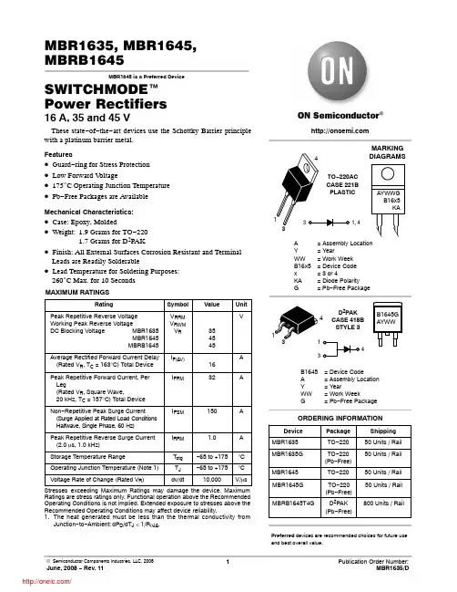
MBR1635, MBR1645, MBRB1645MBR1645 is a Preferred Device SWITCHMODE EPower Rectifiers16 A, 35 and 45 VThese state−of−the−art devices use the Schottky Barrier principle with a platinum barrier metal.Features•Guard−ring for Stress Protection•Low Forward V oltage•175°C Operating Junction Temperature•Pb−Free Packages are AvailableMechanical Characteristics:•Case: Epoxy, Molded•Weight:1.9 Grams for TO−2201.7 Grams for D2PAK•Finish: All External Surfaces Corrosion Resistant and Terminal Leads are Readily Solderable•Lead Temperature for Soldering Purposes:260°C Max. for 10 SecondsMAXIMUM RATINGSRating Symbol Value UnitPeak Repetitive Reverse Voltage Working Peak Reverse VoltageDC Blocking Voltage MBR1635MBR1645MBRB1645V RRMV RWMV R354545VAverage Rectified Forward Current Delay (Rated V R, T C = 163°C) Total Device I F(AV)16APeak Repetitive Forward Current, PerLeg(Rated V R, Square Wave,20 kHz, T C = 157°C) Total DeviceI FRM32ANon−Repetitive Peak Surge Current (Surge Applied at Rated Load Conditions Halfwave, Single Phase, 60 Hz)IFSM150APeak Repetitive Reverse Surge Current(2.0 m s, 1.0 kHz)I RRM 1.0A Storage Temperature Range T stg−65 to +175°C Operating Junction Temperature (Note 1)T J−65 to +175°C Voltage Rate of Change (Rated V R)dv/dt10,000V/m s Stresses exceeding Maximum Ratings may damage the device. Maximum Ratings are stress ratings only. Functional operation above the Recommended Operating Conditions is not implied. Extended exposure to stresses above the Recommended Operating Conditions may affect device reliability.1.The heat generated must be less than the thermal conductivity fromJunction−to−Ambient: dP D/dT J < 1/R q JA.Device Package ShippingORDERING INFORMATIONMBR1635TO−22050 Units / RailMBR1635G TO−220(Pb−Free)50 Units / RailPreferred devices are recommended choices for future use and best overall value.1, 4MARKINGDIAGRAMSA= Assembly LocationY= YearWW= Work WeekB16x5= Device Codex= 3 or 4KA= Diode PolarityG= Pb−Free PackageMBR1645TO−22050 Units / Rail MBR1645G TO−220(Pb−Free)50 Units / RailB1645GAYWWD2PAKCASE 418BSTYLE 34B1645= Device CodeA= Assembly LocationY= YearWW= Work WeekG= Pb−Free PackageMBRB1645T4G D2PAK(Pb−Free)800 Units / Rail34THERMAL CHARACTERISTICSCharacteristic Symbol Value Unit Maximum Thermal Resistance, Junction−to−Case R q JC 1.5°C/W ELECTRICAL CHARACTERISTICSCharacteristic Symbol Value UnitMaximum Instantaneous Forward Voltage (Note 2) (i F = 16 Amps, T C = 125°C)(i F = 16 Amps, T C = 25°C)v F0.570.63VMaximum Instantaneous Reverse Current (Note 2) (Rated dc Voltage, T C = 125°C)(Rated dc Voltage, T C = 25°C)i R400.2mA2.Pulse Test: Pulse Width = 300 m s, Duty Cycle ≤2.0%.Figure 1. Typical Forward Voltage Figure 2. Typical Reverse Currentv F , INSTANTANEOUS FORWARD VOLTAGE (V)10070205010V R , REVERSE VOLTAGE (V)i F , I N S T A N T A N E O U S F O R W A R D C U R R E N T (A )7.05.03.02.01.030 1.0E −1.0E −1.0E −1.0E −1.0E −1.0E −1.0E −R Figure 3. Current Derating, Case, Per LegFigure 4. Current Derating, AmbientFigure 5. Forward Power DissipationI F(AV), AVERAGE FORWARD CURRENT (A)168.06.04.02.00P 141012, A V E R A G E P O W E R D I S S I P A T I O N (W )F (A V E )T C , CASE TEMPERATURE (°C)T A , AMBIENT TEMPERATURE (°C)02468I F (A V ), A V E R A G E F O R W A R D C U R R E N T (A )I F (A V ), A V E R A G E F O R W A R DC U R R E N T (A )10121410121416182022242628161820STYLE 3:PIN 1.ANODE2.CATHODE3.ANODE4.CATHODED 2PAK CASE 418B −04ISSUE Jǒmm inchesǓ*For additional information on our Pb −Free strategy and solderingdetails, please download the ON Semiconductor Soldering and Mounting Techniques Reference Manual, SOLDERRM/D.V DIM MIN MAX MIN MAX MILLIMETERS INCHES A 0.3400.3808.649.65B 0.3800.4059.6510.29C 0.1600.190 4.06 4.83D 0.0200.0350.510.89E 0.0450.055 1.14 1.40G 0.100 BSC 2.54 BSC H 0.0800.110 2.03 2.79J 0.0180.0250.460.64K 0.0900.110 2.29 2.79S 0.5750.62514.6015.88V0.0450.0551.14 1.40NOTES:1.DIMENSIONING AND TOLERANCING PER ANSI Y14.5M, 1982.2.CONTROLLING DIMENSION: INCH.3.418B −01 THRU 418B −03 OBSOLETE,NEW STANDARD 418B −04.F 0.3100.3507.878.89L 0.0520.072 1.32 1.83M 0.2800.3207.118.13N 0.197 REF 5.00 REF P0.079 REF 2.00 REF R 0.039 REF 0.99 REF VARIABLEVIEW W −WVIEW W −WVIEW W −W123TO −220PLASTIC CASE 221B −04ISSUE EUDIM MIN MAX MIN MAX MILLIMETERSINCHES A 0.5950.62015.1115.75B 0.3800.4059.6510.29C 0.1600.190 4.06 4.82D 0.0250.0350.640.89F 0.1420.161 3.61 4.09G 0.1900.210 4.83 5.33H 0.1100.130 2.79 3.30J 0.0140.0250.360.64K 0.5000.56212.7014.27L 0.0450.060 1.14 1.52Q 0.1000.120 2.54 3.04R 0.0800.110 2.04 2.79S 0.0450.055 1.14 1.39T 0.2350.255 5.97 6.48U0.0000.0500.000 1.27NOTES:1.DIMENSIONING AND TOLERANCING PER ANSI Y14.5M, 1982.2.CONTROLLING DIMENSION: INCH.ON Semiconductor and are registered trademarks of Semiconductor Components Industries, LLC (SCILLC). SCILLC reserves the right to make changes without further noticeto any products herein. SCILLC makes no warranty, representation or guarantee regarding the suitability of its products for any particular purpose, nor does SCILLC assume any liability arising out of the application or use of any product or circuit, and specifically disclaims any and all liability, including without limitation special, consequential or incidental damages.“Typical” parameters which may be provided in SCILLC data sheets and/or specifications can and do vary in different applications and actual performance may vary over time. All operating parameters, including “Typicals” must be validated for each customer application by customer’s technical experts. SCILLC does not convey any license under its patent rights nor the rights of others. SCILLC products are not designed, intended, or authorized for use as components in systems intended for surgical implant into the body, or other applications intended to support or sustain life, or for any other application in which the failure of the SCILLC product could create a situation where personal injury or death may occur. Should Buyer purchase or use SCILLC products for any such unintended or unauthorized application, Buyer shall indemnify and hold SCILLC and its officers, employees, subsidiaries, affiliates,and distributors harmless against all claims, costs, damages, and expenses, and reasonable attorney fees arising out of, directly or indirectly, any claim of personal injury or death associated with such unintended or unauthorized use, even if such claim alleges that SCILLC was negligent regarding the design or manufacture of the part. SCILLC is an Equal Opportunity/Affirmative Action Employer. This literature is subject to all applicable copyright laws and is not for resale in any manner.PUBLICATION ORDERING INFORMATIONSWITCHMODE is a trademark of Semiconductor Components Industries, LLC.分销商库存信息:ONSEMIMBR1645G MBR1635G MBRB1645T4G。

DISCLAIMERFAIRCHILD SEMICONDUCTOR RESERVES THE RIGHT TO MAKE CHANGES WITHOUT FURTHER NOTICE TO ANY PRODUCTS HEREIN TO IMPROVE RELIABILITY, FUNCTION OR DESIGN. FAIRCHILD DOES NOT ASSUME ANY LIABILITY ARISING OUT OF THE APPLICATION OR USE OF ANY PRODUCT OR CIRCUIT DESCRIBED HEREIN;NEITHER DOES IT CONVEY ANY LICENSE UNDER ITS PATENT RIGHTS, NOR THE RIGHTS OF OTHERS.LIFE SUPPORT POLICYFAIRCHILD’S PRODUCTS ARE NOT AUTHORIZED FOR USE AS CRITICAL COMPONENTS IN LIFE SUPPORT DEVICES OR SYSTEMS WITHOUT THE EXPRESS WRITTEN APPROVAL OF FAIRCHILD SEMICONDUCTOR CORPORATION.As used herein:1. Life support devices or systems are devices or systems which, (a) are intended for surgical implant into the body,or (b) support or sustain life, or (c) whose failure to perform when properly used in accordance with instructions for use provided in the labeling, can be reasonably expected to result in significant injury to the user.2. A critical component is any component of a life support device or system whose failure to perform can be reasonably expected to cause the failure of the life support device or system, or to affect its safety or effectiveness.PRODUCT STATUS DEFINITIONS Definition of TermsDatasheet Identification Product Status DefinitionAdvance InformationFormative or In Design This datasheet contains the design specifications for product development. Specifications may change in any manner without notice.PreliminaryFirst ProductionThis datasheet contains preliminary data, andsupplementary data will be published at a later date.Fairchild Semiconductor reserves the right to make changes at any time without notice in order to improve design.No Identification Needed Full ProductionThis datasheet contains final specifications. Fairchild Semiconductor reserves the right to make changes at any time without notice in order to improve design.Obsolete Not In ProductionThis datasheet contains specifications on a product that has been discontinued by Fairchild semiconductor.The datasheet is printed for reference information only.TRADEMARKSThe following are registered and unregistered trademarks Fairchild Semiconductor owns or is authorized to use and is not intended to be an exhaustive list of all such trademarks.FAST ®FASTr™FPS™FRFET™GlobalOptoisolator™GTO™HiSeC™I 2C™i-Lo ™ImpliedDisconnect™ISOPLANAR™LittleFET™MICROCOUPLER™MicroFET™MicroPak™MICROWIRE™MSX™MSXPro™OCX™OCXPro™OPTOLOGIC ®OPTOPLANAR™PACMAN™POP™Power247™PowerSaver™PowerTrench ®QFET ®QS™QT Optoelectronics™Quiet Series™RapidConfigure™RapidConnect™µSerDes™SILENT SWITCHER ®SMART START™SPM™Stealth™SuperFET™SuperSOT™-3SuperSOT™-6SuperSOT™-8SyncFET™TinyLogic ®TINYOPTO™TruTranslation™UHC™UltraFET ®VCX™A CEx™ActiveArray™Bottomless™CoolFET™CROSSVOLT ™DOME™EcoSPARK™E 2CMOS™EnSigna™FACT™FACT Quiet Series™Across the board. Around the world.™The Power Franchise ®Programmable Active Droop™分销商库存信息: FAIRCHILD MBRS140。

MBR1545CTP SWITCHMODE™Power Rectifiering the Schottky Barrier principle with a platinum barrier metal. These state–of–the–art devices have the following features:•Center–Tap Configuration•Guardring for Stress Protection•Low Forward V oltage•150°C Operating Junction Temperature•Epoxy Meets UL94, VO at 1/8″Mechanical Characteristics:•Case: Epoxy, Molded•Weight: 1.9 grams (approximately)•Finish: All External Surfaces Corrosion Resistant and Terminal Leads are Readily Solderable•Lead Temperature for Soldering Purposes:260°C Max. for 10 Seconds•Shipped 50 units per plastic tube•Marking: B1545PMAXIMUM RATINGSDevice Package Shipping ORDERING INFORMATIONMBR1545CTP TO–22050 Units/RailTHERMAL CHARACTERISTICS (Per Diode)ELECTRICAL CHARACTERISTICS (Per Diode)Figure 1. Maximum Forward Voltage V F , INSTANTANEOUS FORWARD VOLTAGE (VOLTS)100101Figure 2. Typical Forward Voltage0.1i F , I N ST A N T A N E O U S FO R W A R D C U R R E N T (A )V F , INSTANTANEOUS FORWARD VOLTAGE (VOLTS)1010.1i F , I N S T A N T A N E O U S F O R W A R D C U R R E N T (A )100Figure 3. Typical Reverse Current V R , REVERSE VOLTAGE (VOLTS)Figure 4. Typical CapacitanceV R , REVERSE VOLTAGE (VOLTS)20010020151000353025508005I R , R E V E R S E C U R R E N T (A )4540400300500700600C , C A P A C I T A N C E (p F )Figure 5. Current Derating, Case, Per Diode T C , CASE TEMPERATURE (°C)Figure 6. Forward Power Dissipation, Per DiodeI F(AV), AVERAGE FORWARD CURRENT (AMPS)210843576I F (A V ), A V E R A G E F O R W A R D C U R R E N T (A )P F (A V ), A V E R A G E F O R W A R D P O W E R D I S S I P A T I O N (W )PACKAGE DIMENSIONSTO–220THREE–LEADTO–220ABCASE 221A–09ISSUE AASWITCHMODE is a trademark of Semiconductor Components Industries, LLC.ON Semiconductor and are trademarks of Semiconductor Components Industries, LLC (SCILLC). SCILLC reserves the right to make changes without further notice to any products herein. SCILLC makes no warranty, representation or guarantee regarding the suitability of its products for any particular purpose, nor does SCILLC assume any liability arising out of the application or use of any product or circuit, and specifically disclaims any and all liability, including without limitation special, consequential or incidental damages. “Typical” parameters which may be provided in SCILLC data sheets and/or specifications can and do vary in different applications and actual performance may vary over time. All operating parameters, including “Typicals” must be validated for each customer application by customer’s technical experts. SCILLC does not convey any license under its patent rights nor the rights of others.SCILLC products are not designed, intended, or authorized for use as components in systems intended for surgical implant into the body, or other applications intended to support or sustain life, or for any other application in which the failure of the SCILLC product could create a situation where personal injury or death may occur. Should Buyer purchase or use SCILLC products for any such unintended or unauthorized application, Buyer shall indemnify and hold SCILLC and its officers, employees, subsidiaries, affiliates, and distributors harmless against all claims, costs, damages, and expenses, and reasonable attorney fees arising out of, directly or indirectly, any claim of personal injury or death associated with such unintended or unauthorized use, even if such claim alleges that SCILLC was negligent regarding the design or manufacture of the part. SCILLC is an Equal Opportunity/Affirmative Action Employer. PUBLICATION ORDERING INFORMATIONCENTRAL/SOUTH AMERICA:Spanish Phone:303–308–7143 (Mon–Fri 8:00am to 5:00pm MST)Email:ONlit–spanish@Toll–Free from Mexico: Dial 01–800–288–2872 for Access –then Dial 866–297–9322ASIA/PACIFIC: LDC for ON Semiconductor – Asia SupportPhone:1–303–675–2121 (Tue–Fri 9:00am to 1:00pm, Hong Kong Time)Toll Free from Hong Kong & Singapore:001–800–4422–3781Email: ONlit–asia@JAPAN: ON Semiconductor, Japan Customer Focus Center4–32–1 Nishi–Gotanda, Shinagawa–ku, Tokyo, Japan 141–0031Phone: 81–3–5740–2700。

MBR1635 - MBR1660MBR1635 - MBR1660 Rev. A©1999 Fairchild Semiconductor CorporationMBR1635 - MBR1660 Rev. ATRADEMARKSACEx™CoolFET™CROSSVOLT™E 2CMOS TM FACT™FACT Quiet Series™FAST ®FASTr™GTO™HiSeC™The following are registered and unregistered trademarks Fairchild Semiconductor owns or is authorized to use and is not intended to be an exhaustive list of all such trademarks.LIFE SUPPORT POLICYFAIRCHILD’S PRODUCTS ARE NOT AUTHORIZED FOR USE AS CRITICAL COMPONENTS IN LIFE SUPPORTDEVICES OR SYSTEMS WITHOUT THE EXPRESS WRITTEN APPROV AL OF FAIRCHILD SEMICONDUCTOR CORPORA TION.As used herein:ISOPLANAR™MICROWIRE™POP™PowerTrench™QS™Quiet Series™SuperSOT™-3SuperSOT™-6SuperSOT™-8TinyLogic™1. Life support devices or systems are devices or systems which, (a) are intended for surgical implant intothe body, or (b) support or sustain life, or (c) whosefailure to perform when properly used in accordancewith instructions for use provided in the labeling, can be reasonably expected to result in significant injury to the user.2. A critical component is any component of a lifesupport device or system whose failure to perform can be reasonably expected to cause the failure of the life support device or system, or to affect its safety or effectiveness.PRODUCT STATUS DEFINITIONS Definition of TermsDatasheet Identification Product Status Definition Advance InformationPreliminary No Identification Needed Obsolete This datasheet contains the design specifications for product development. Specifications may change in any manner without notice.This datasheet contains preliminary data, andsupplementary data will be published at a later date.Fairchild Semiconductor reserves the right to make changes at any time without notice in order to improve design.This datasheet contains final specifications. Fairchild Semiconductor reserves the right to make changes at any time without notice in order to improve design.This datasheet contains specifications on a product that has been discontinued by Fairchild semiconductor.The datasheet is printed for reference information only.Formative or In DesignFirst ProductionFull ProductionNot In ProductionDISCLAIMERFAIRCHILD SEMICONDUCTOR RESERVES THE RIGHT TO MAKE CHANGES WITHOUT FURTHER NOTICE TO ANY PRODUCTS HEREIN TO IMPROVE RELIABILITY , FUNCTION OR DESIGN. FAIRCHILD DOES NOT ASSUME ANY LIABILITY ARISING OUT OF THE APPLICATION OR USE OF ANY PRODUCT OR CIRCUIT DESCRIBED HEREIN; NEITHER DOES IT CONVEY ANY LICENSE UNDER ITS PATENT RIGHTS, NOR THE RIGHTS OF OTHERS.。