MEMS数字麦克风基本知识课件
- 格式:ppt
- 大小:2.31 MB
- 文档页数:12
MEMS麦克风•MEMS(微型机电系统)麦克风是基于MEMS技术制造的麦克风,简单的说就是一个电容器集成在微硅晶片上,可以采用表贴工艺进行制造,能够承受很高的回流焊温度,容易与CMOS 工艺及其它音频电路相集成, 并具有改进的噪声消除性能与良好的RF 及EMI 抑制性能.MEMS麦克风的全部潜能还有待挖掘,但是采用这种技术的产品已经在多种应用中体现出了诸多优势,特别是中高端手机应用中。
目录•MEMS麦克风的发展前景MEMS麦克风的优势•目前,实际使用的大多数麦克风都是ECM(驻极体电容器)麦克风,这种技术已经有几十年的历史。
ECM 的工作原理是利用驻有永久电荷的聚合材料振动膜。
与ECM的聚合材料振动膜相比,MEMS麦克风在不同温度下的性能都十分稳定,其敏感性不会受温度、振动、湿度和时间的影响。
由于耐热性强,MEMS麦克风可承受260℃的高温回流焊,而性能不会有任何变化。
由于组装前后敏感性变化很小,还可以节省制造过程中的音频调试成本。
MEMS麦克风需要ASIC提供的外部偏置,而ECM没有这种偏置。
有效的偏置将使MEMS麦克风在整个操作温度范围内都可保持稳定的声学和电气参数,还支持具有不同敏感性的麦克风设计。
传统ECM的尺寸通常比MEMS麦克风大,并且不能进行SMT(表面贴装技术)操作。
在MEMS麦克风的制造过程中,SMT回流焊简化了制造流程,可以省略一个目前通常以手工方式进行的制造步骤。
在ECM麦克风内,必须添加进行信号处理的电子元件;而在MEMS麦克风中,只需在芯片上添加额外的专用功能即可。
与ECM相比,这种额外功能的优点是使麦克风具有很高的电源抑制比,能够有效抑制电源电压的波动。
另一个优点是,集成在芯片上的宽带RF抑制功能,这一点不仅对手机这样的RF应用尤其重要,而且对所有与手机操作原理类似的设备(如助听器)都非常重要。
MEMS麦克风的小型振动膜还有另一个优点,直径不到1mm的小型薄膜的重量同样轻巧,这意味着,与ECM相比,MEMS麦克风会对由安装在同一PCB上的扬声器引起的PCB 噪声产生更低的振动耦合。
February 2017DocID025704 Rev 2 1/20 AN4426 Application note Tutorial for MEMS microphonesIntroductionThis application note serves as a tutorial for MEMS microphones, providing general characteristics of these devices, both acoustic and mechanical, as well as summarizing the portfolio available from ST. MEMS microphones target all audio applications where small size, high sound quality, reliability and affordability are key requirements.ST's MEMS microphones are designed, developed and manufactured within ST, creating an industry-unique, vertically integrated supply chain. Both analog and digital-input, top and bottom-port solutions are available.Our best-in-class AOP and SNR make ST’s MEMS microphones suitable for applications that require a very high dynamic range, improving the audio experience in any environment. Matching very tightsensitivity allows optimizing beamforming and noise cancelling algorithms for multi-microphone arrays. Low power consumption allows extending battery life.Contents AN4426 Contents1Mechanical specifications, construction details (4)2Acoustic parameters (11)2.1Sensitivity (11)2.2Directionality (11)2.3SNR (12)2.4Dynamic range and acoustic overload point (12)2.5Equivalent input noise (13)2.6Frequency response (15)2.7Total harmonic distortion (16)2.8PSRR and PSR (16)3MEMS microphone portfolio (17)4Revision history (19)2/20 DocID025704 Rev 2AN4426 List of figures List of figuresFigure 1: MEMS microphone inside package (4)Figure 2: MEMS transducer mechanical specifications (4)Figure 3: Capacitance change principle (5)Figure 4: 4 x 5 package (5)Figure 5: 3 x 4 metal cap package - bottom port (6)Figure 6: 3 x 4 package - top port (6)Figure 7: 2 x 3 package - bottom port (7)Figure 8: Faraday cage in ST’s MEMS microphones (7)Figure 9: RF immunity simulation (8)Figure 10: EMC test setup (8)Figure 11: RF test disturbance signal with sinusoidal pattern (9)Figure 12: RF immunity test results - MP34DT04 (9)Figure 13: RF test disturbance signal @ 217 Hz burst pattern (10)Figure 14: RF immunity of analog differential microphones (10)Figure 15: Omnidirectional microphone (11)Figure 16: A-weighted filter response (12)Figure 17: Acoustic and electrical relationship - analog (13)Figure 18: Acoustic and electrical relationship - digital (14)Figure 19: MP45DT02-M frequency response (15)Figure 20: MEMS microphone portfolio (17)Figure 21: MEMS microphone notation (17)DocID025704 Rev 2 3/201 Mechanical specifications, construction detailsA microphone is a dual-die device consisting of two components, the integrated circuit andthe sensor, which are housed in a package using techniques that are proprietary to ST.ASICintegratedThe sensor uses MEMS technology (Micro-Electrical-Mechanical Systems) and it isbasically a silicon capacitor. The capacitor consists of two silicon plates/surfaces. Oneplate is fixed while the other one is movable (respectively, the green plate and the grey oneshown in the following figure). The fixed surface is covered by an electrode to make itconductive and is full of acoustic holes which allow sound to pass through. The movableplate is able to move since it is bonded at only one side of its structure. A ventilation hole,allows the air compressed in the back chamber to flow out and consequently allows themembrane to move back. The chamber allows the membrane to move inside but also, incombination with the chamber created by the package will affect the acoustic performanceof the microphones in terms of frequency response and SNR.Figure 2: MEMS transducer mechanical specificationsSo basically the microphone MEMS sensor is a variable capacitor where the transductionprinciple is the coupled capacitance change between a fixed plate (back plate) and amovable plate (membrane) caused by the incoming wave of the sound.4/20 DocID025704 Rev 2Figure 3: Capacitance change principleThe integrated circuit converts the change of the polarized MEMS capacitance into a digital (PDM modulated) or analog output according to the microphone type. Finally the MEMS microphone is housed in a package with the sound inlet placed in the top or in the bottom part of the package, hence the top-port or bottom-port nomenclature of the package. ST manufactures microphones using industry-wide techniques, but also has developed innovative packaging to achieve improved performance of the microphones. Packaging techniques will be discussed in further detail.The 4x5 package is widely used to house the digital microphone MP45DT02-M. It is a common packaging technique in a top-port configuration where the ASIC is placed under the sound inlet with glue on top (glob top) in order to protect the circuit from light and the MEMS sensor is placed beside the integrated circuit. The two silicon components are fixed to the substrate and the pads of the device are on the bottom side. The resonant chambers are identified depending on the position of each chamber with respect to the membrane and the incoming sound. In this case, considering the incoming direction of the sound, the front chamber is created by the package and the chamber inside the MEMS, behind the MEMS membrane, is the back chamber. This configuration allows protecting the MEMS from dust and particles falling into the package but results in a low SNR and frequency response with a peak in the audio band.Figure 4: 4 x 5 packageThe 3x4 package is used in ST to produce both the bottom and the top-port digital microphones, MP34DB02 and MP34DT01-M, MP34DT04/-C1, and MP34DT05. Considering the bottom configuration first, this structure is depicted in the following figure. The ASIC and the MEMS sensor are fixed to the substrate and the pads of the device are on bottom side as well. The sound inlet is obtained by drilling the substrate according to the position of the MEMS sensor. The package encloses all the components. In this configuration the front chamber is the cavity of the MEMS sensor and the package creates the back chamber. This design optimizes the acoustic performance of the microphone in terms of SNR and also allows obtaining a flat response across the entire audio band. The drawback of this solution is represented by the assembly of this microphone. Usually theDocID025704 Rev 2 5/20bottom-port microphones are soldered on the PCB. The thickness of the board modifies thevolume of the front chamber, degrading the flat response of this type of microphone (referto AN4427, “Gasket design for optimal acoustic performance in MEMS microphones” fordetails). In order to minimize the artifacts caused by this environment, a flex cable isrecommended to be used. Additionally, the bottom-port microphones have a ringed metalpad around the hole. A very careful soldering process is required to avoid dust or solderingpaste from entering in the sound port, damaging the MEMS membrane.Figure 5: 3 x 4 metal cap package - bottom portThe 3x4 top-port configuration is basically a mirrored bottom-port microphone. The ASICand the sensor are placed close to each other, the sensor is still under the sound inlet butthese two components are attached to the top of the structure, in other words, the ASICand MEMS are fixed to the package lid, not to the substrate. The pads are on the substrateand thus on the bottom side of the microphone. This configuration, covered by ST patents,allows optimizing all the benefits of the bottom-port microphone in terms of acousticperformance (i.e. maximized SNR and flat band) and all the benefits related to the top-portconfiguration during the assembly process.Figure 6: 3 x 4 package - top port6/20 DocID025704 Rev 2A smaller package, 2.5 x 3.35 mm, has been introduced in ST's product portfolio (for simplicity referred to as 2x3, see Figure 7: "2 x 3 package - bottom port"). This package is a bottom-port configuration with the same internal construction as the 3 x 4 bottom-port package and it is used for the analog differential microphones MP23AB01DM/DH and analog single-ended microphone MP23AB02B. As a result of the 2x3 bottom-port package and differential output configuration, the MP23AB01DH is the best microphone provided by ST in terms of SNR and AOP.Figure 7: 2 x 3 package - bottom portMEMS microphones housed in a plastic package are protected from radiated disturbances by embedding in the plastic package a metal shield which serves as a Faraday cage. The model in the following figure shows how the Faraday cage is implemented in ST’s plastic packages.Figure 8: Faraday cage in ST’s MEMS microphonesThe next figure shows the simulation of an electric field in open space. By applying an electric field source outside the microphone package, the Faraday cage is able to considerably attenuate the field inside the microphone structure. The temperature grade of the E field is an easy way to plot the results.DocID025704 Rev 2 7/20Figure 9: RF immunity simulationIn addition to the simulation, ST has a dedicated test to evaluate immunity, “Microphonedurability to EMC disturbances”.Microphones are subjected to RF disturbances using a proper jig with the following setup.Basically the test consists of placing the microphone under an antenna radiating adisturbance signal of 1 kHz AM modulated in the range [0.8, 3] GHz. The RF amplitudediffers depending on the frequency range according to the following criteria:•+33 dBm in the range [0.8, 2.4]•+17 dBm in the range [2.4, 3.0]8/20 DocID025704 Rev 2Figure 11: RF test disturbance signal with sinusoidal patternThe carrier of the disturbance is 1 kHz since it is an audio signal. Hence, the RF immunity of the microphone is evaluated by measuring the residual of the carrier at the output of the microphone. The next figure shows the result of the peak at 1 kHz measured when applying the RF disturbance on top of an MP34DT04.In parallel with the sinusoidal pattern, another 217 Hz burst pattern used to test the RF immunity is shown in the following figure.•The RF amplitude (power): +33 dBm•Carrier frequency: 700 MHz ~ 2.5 GHz•GSM burst frequency: 217 Hz pattern (see below)DocID025704 Rev 2 9/20Figure 13: RF test disturbance signal @ 217 Hz burst patternFigure 14: RF immunity of analog differential microphones10/20 DocID025704 Rev 2AN4426Acoustic parametersDocID025704 Rev 211/202Acoustic parameters2.1SensitivityThe sensitivity is the electrical signal at the microphone output to a given acoustic pressure as input. The reference of acoustic pressure is 1 Pa or 94 dBSPL @ 1 kHz. The sound pressure level, expressed in decibel, dBSPL=20*Log(P/Po) where Po = 20 µPa is the threshold of hearing. 20*Log(1Pa/20µPa) = 94 dBSPL • For analog microphones the sensitivity is expressed in mV RMS /Pa or dBV/Pa •For digital microphones the sensitivity is expressed in dBFSdBV ≠ dBFS. It is not correct to compare different units. As given in the above equations, dBV is in reference to 1V RMS instead of dBFS where the reference is the digital full scale.2.2 DirectionalityThe directionality indicates the variation of the sensitivity response with respect to thedirection of the arrival of the sound. MEMS microphones from ST are omnidirectional which means that there is no sensitivity change to every different position of the source of thesound in space. The directionality can be indicated in a Cartesian axis as sensitivity drift vs. angle or in a polar diagram showing the sensitivity pattern response in space.The following figure depicts the directionality in these two reference systems.Figure 15: Omnidirectional microphoneAcoustic parametersAN442612/20DocID025704 Rev 22.3 SNRThe signal-to-noise ratio specifies the ratio between a given reference signal to the amount of residual noise at the microphone output. The reference signal is the standard signal at the microphone output when the sound pressure is 1Pa @ 1 kHz (microphone sensitivity). The noise signal (residual noise) is the microphone electrical output at silence.This parameter includes both the noise of the MEMS element and the ASIC. Concerning this sum, the main contribution to noise is given by the MEMS sensor, the integrated circuit contribution can be considered negligible. Typically, the noise level is measured in an anechoic environment and A-weighting the acquisition. The A-weighted filter corresponds to the human ear frequency response.Figure 16: A-weighted filter response2.4 Dynamic range and acoustic overload pointThe dynamic range is the difference between the minimum and maximum signal that the microphone is able to generate as output. • The minimum signal is the smallest audio signal that the microphone can generate distinctly from noise. In other words, the minimum signal is equivalent to the residual noise.•The maximum audio signal is that which the microphone can generate withoutdistortion. It is also called acoustic overload point (AOP). Actually, the specification allows up to 10% in terms of distortion at the acoustic overload point.AN4426 Acoustic parameters2.5 Equivalent input noiseA microphone is a sound-to-electricity transducer which means that any output signalcorresponds to a specific sound as input. The equivalent input noise (EIN) is the acousticlevel, expressed in dBSPL, corresponding to the residual noise as output.For example, a digital microphone with a sensitivity of -26 dBFS and a 63 dB as SNR:Residual noise = -26 - 63 = -89 dBFS this sum transposed in the acoustic domain is:EIN = 94 - 63= 31 dBSPLThe following figures summarize the relationship between the acoustic and electricdomains related to each of the parameters listed above. Figure 17: "Acoustic and electricalrelationship - analog" and Figure 18: "Acoustic and electrical relationship - digital" illustratethis for analog and digital microphones, respectively.Figure 17: Acoustic and electrical relationship - analogDocID025704 Rev 2 13/20Acoustic parametersAN442614/20DocID025704 Rev 29030-90-3094dBSPL AOPS N R =63d B-26dBFSD y n a m i c R a n g e =89d BSensitivity EIN Residual noiseAN4426 Acoustic parameters 2.6 Frequency responseThe frequency response of a microphone in terms of magnitude indicates the sensitivityvariation across the audio band. This parameter also describes the deviation of the outputsignal from the reference 0 dB. Typically, the reference for this measurement is exactly thesensitivity of the microphone @ 0 dB = 94 dBSPL @ 1 kHz. The frequency response of amicrophone can vary across the audio frequency band depending on three parameters: theventilation hole, the front chamber geometry, and back chamber geometry. The ventilationhole and the back chamber geometry have an impact on the behavior at low frequencieswhile the behavior at high frequencies depends on the geometry of the front chamber only.Behavior at high frequencies can be a resonance peak caused by the Helmholtz effect.This resonance is the phenomenon of air resonance in a cavity. As a matter of fact, itdepends on the dimension of the front chamber of the microphone, representing the soundcavity in which the air resonates. A microphone with a flat frequency response is suitablewhen natural sound and high intelligibility of the system is required. The following figureshows the response of the MP45DT02-M. It shows a roll-off at low frequencies and a peakaround 18 kHz caused by the large front chamber of this microphone.Figure 19: MP45DT02-M frequency responseThe frequency response of a microphone in terms of phase indicates the phase distortionintroduced by the microphone. In other words, the delay between the sound wave movingthe microphone membrane and the electrical signal at the microphone output results in thatthis parameter includes both the distortion due to the membrane and the ASIC.DocID025704 Rev 2 15/20Acoustic parametersAN442616/20DocID025704 Rev 22.7 Total harmonic distortionTHD is the measurement of the distortion affecting the electrical output signal of themicrophone given an undistorted acoustic signal as input. THD+N is expressed as a ratio of the integer in a specified band of the power of the harmonics plus the power of noise and the power of the undistorted signal (fundamental). Equation 1TTTTTT +NN (%)=∑PPPPPPPPPP (TTHHPPHHPPHHHH HH HH )+PPPPPPPPPP (NNPPHH HH PP )NN nn−1PPPPPPPPPP (FFFFHHFFHHHHPPHHFFHHFF )Typically ST indicates the THD+N measured in the (50 Hz - 4 kHz) band for a given undistorted signal 1 kHz @ 100 dBSPL.2.8 PSRR and PSRPSRR indicates the capability of the ASIC to reject noise added to the supply voltage. To evaluate this parameter, a tone of V IN = 100 mVpk-pk @ 217 Hz (GSM switching frequency in phone applications) is added to the power supply and then the amplitude of the output is measured. The added noise can be either a square wave or sinusoidal wave. Typically the square wave is preferred since it is the worst case.PSRR is the ratio of the residual noise amplitude at the microphone output (V OUT @ 217 Hz) to the added spurious signal on the supply voltage. It is typically expressed in dB as given in the equation below: Equation 2PPPPPPPP =20 xx log �(VV OOOOOO @217TTHH )(VV IINN @217TTHH )�The capability of the integrated circuit to reject noise added to the supply voltage can also be expressed with another parameter that is the PSR. Basically it is simply a measurement of the output when noise of 100 mVpk-pk @ 217 Hz is superposed to the supply voltage. Consequently expressed in dB as given in the equation below: Equation 3 PPPPPP =20 xx log[VV OOOOOO @217TTHH ]To evaluate either the PSRR or PSR, proper sealing of the sound inlet or measurements performed in an anechoic chamber are recommended to avoid mixing the superimposed noise with that of the noise floor of the output. Finally, in the microphone datasheets PSR is commonly given instead of PSRR.AN4426 MEMS microphone portfolio3 MEMS microphone portfolioFigure 20: MEMS microphone portfolioST’s portfolio includes digital and analog microphones. The commercial products arenamed using the notation depicted in the following figure.Figure 21: MEMS microphone notationDocID025704 Rev 2 17/20MEMS microphone portfolio AN442618/20DocID025704 Rev 2The following table provides a complete overview of the microphones offered by ST. Additionally it serves as a summary for selecting the appropriate microphone among the ST portfolio as the features of both digital and analog microphones are given.Table 1: Features of MEMS microphonesParameter MP45DT02-M MP34DB02 MP34DT01-M MP34DT04 MP34DT04-C1 MP34DT05 MP23AB02B MP23AB01DM MP23AB01DH Sensitivity -26 dBFS -26 dBFS -26 dBFS -26 dBFS -26 dBFS -26 dBFS -38 dBV -38 dBV -38 dBV Directivity OmnidirectionalOmnidirectional OmnidirectionalOmnidirectionalOmnidirectionalOmnidirectionalOmnidirectionalOmnidirectionalOmnidirectionalSNR 61 dB 62.5 dB 61 dB 64 dB 64 dB 64 dB 64 dB 64 dB 65 dB AOP 120 dBSPL 120 dBSPL 120 dBSPL 120 dBSPL 120 dBSPL 122 dBSPL 125 dBSPL 130 dBSPL 135 dBSPL EIN 33 dB 31.5 dB 33 dB 30 dB 30 dB 30 dB 30 dB 30 dB 29 dB THD+N <5% @ 115 dBSPL <5% @ 115 dBSPL <2% @ 115 dBSPL <5% @ 115 dBSPL <5% @ 115 dBSPL <6% @ 120 dBSPL <2% @ 120 dBSPL <10% @ 130 dBSPL <5% @ 130 dBSPL PSR -70 dB -86 dB -70 dB -70 dB -70 dB -72 dB -70 dB -85 dB -100 dB Max. current consumption 650 µA 650 µA 600 µA 700 µA 700 µA 650 µA 220 µA 250 µA 250 µA Package dimensions 3.76x4.76x1.25mm3x4x1mm 3x4x1.06mm 3x4x1.095mm 3x4x1.095mm 3x4x1mm 2.5x3.35x0.98mm 2.5x3.35x0.98mm 2.5x3.35x0.98mm Port location Top port Bottom port Top port Top port Top port Top port Bottom port Bottom port Bottom port Operating temperature-30°C<T<+85°C-40°C<T<+85°C-40°C<T<+85°C-40°C<T<+85°C-40°C<T<+85°C-40°C<T<+85°C-40°C<T<+85°C-40°C<T<+85°C-40°C<T<+85°CAN4426Revision historyDocID025704 Rev 219/204 Revision historyTable 2: Document revision historyDate RevisionChanges09-Jan-20141Initial release14-Feb-2017 2Updated part numbers throughout documentUpdated "Introduction" and Section 1: "Mechanical specifications, construction details"Updated Figure 5: "3 x 4 metal cap package - bottom port", Figure 20: "MEMS microphone portfolio", Figure 21: "MEMS microphone notation"Added Figure 7: "2 x 3 package - bottom port",Figure 13: "RF test disturbance signal @ 217 Hz burst pattern", Figure 14: "RF immunity of analog differential microphones" Updated Table 1: "Features of MEMS microphones"AN4426IMPORTANT NOTICE – PLEASE READ CAREFULLYSTMicroelectronics NV and its subsidiaries (“ST”) reserve the right to make changes, corrections, enhancements, modifications, and improvements to ST products and/or to this document at any time without notice. Purchasers should obtain the latest relevant information on ST products before placing orders. ST products are sold pursuant to ST’s terms and conditions of sale in place at the time of order acknowledgement.Purchasers are solely responsible for the choice, selection, and use of ST products and ST assumes no liability for application assistance or the design of Purchasers’ products.No license, express or implied, to any intellectual property right is granted by ST herein.Resale of ST products with provisions different from the information set forth herein shall void any warranty granted by ST for such product.ST and the ST logo are trademarks of ST. All other product or service names are the property of their respective owners.Information in this document supersedes and replaces information previously supplied in any prior versions of this document.© 2017 STMicroelectronics – All rights reserved20/20 DocID025704 Rev 2。


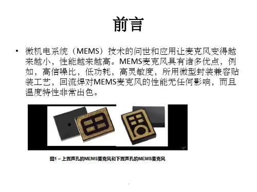

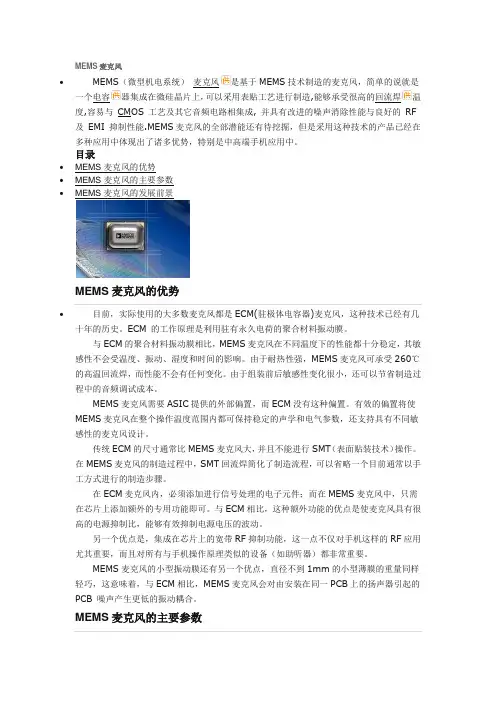
∙MEMS(微型机电系统)麦克风是基于MEMS技术制造的麦克风,简单的说就是一个电容器集成在微硅晶片上,可以采用表贴工艺进行制造,能够承受很高的回流焊温度,容易与 CMOS 工艺及其它音频电路相集成, 并具有改进的噪声消除性能与良好的RF 及EMI 抑制性能.MEMS麦克风的全部潜能还有待挖掘,但是采用这种技术的产品已经在多种应用中体现出了诸多优势,特别是中高端手机应用中。
目录∙MEMS麦克风的优势∙MEMS麦克风的主要参数∙MEMS麦克风的发展前景MEMS麦克风的优势∙目前,实际使用的大多数麦克风都是ECM(驻极体电容器)麦克风,这种技术已经有几十年的历史。
ECM 的工作原理是利用驻有永久电荷的聚合材料振动膜。
与ECM的聚合材料振动膜相比,MEMS麦克风在不同温度下的性能都十分稳定,其敏感性不会受温度、振动、湿度和时间的影响。
由于耐热性强,MEMS麦克风可承受260℃的高温回流焊,而性能不会有任何变化。
由于组装前后敏感性变化很小,还可以节省制造过程中的音频调试成本。
MEMS麦克风需要ASIC提供的外部偏置,而ECM没有这种偏置。
有效的偏置将使MEMS麦克风在整个操作温度范围内都可保持稳定的声学和电气参数,还支持具有不同敏感性的麦克风设计。
传统ECM的尺寸通常比MEMS麦克风大,并且不能进行SMT(表面贴装技术)操作。
在MEMS麦克风的制造过程中,SMT回流焊简化了制造流程,可以省略一个目前通常以手工方式进行的制造步骤。
在ECM麦克风内,必须添加进行信号处理的电子元件;而在MEMS麦克风中,只需在芯片上添加额外的专用功能即可。
与ECM相比,这种额外功能的优点是使麦克风具有很高的电源抑制比,能够有效抑制电源电压的波动。
另一个优点是,集成在芯片上的宽带RF抑制功能,这一点不仅对手机这样的RF应用尤其重要,而且对所有与手机操作原理类似的设备(如助听器)都非常重要。
MEMS麦克风的小型振动膜还有另一个优点,直径不到1mm的小型薄膜的重量同样轻巧,这意味着,与ECM相比,MEMS麦克风会对由安装在同一PCB上的扬声器引起的PCB 噪声产生更低的振动耦合。