HA2089 烟感专用MICROCHIP单片机规格书
- 格式:pdf
- 大小:155.67 KB
- 文档页数:4

微芯科技:家用独立式红外烟雾报警器控制方案
众所周知,在中国,如办公、宾馆、商业和娱乐等公共场所,都必须要求安装烟雾报警器及消防设施;而在如公寓、别墅和宿舍等民用场所则没有强制要求。
但是,在欧美发达国家,居民的消防意识比较强,通常住宅中也会安装烟雾报警器,报警器的探头一般采用独立式,其工作原理与我们常见的集控式探头非常类似,也是由红外或者离子传感器、电子控制单元以及蜂鸣器组成,不同的是由单独的电池供电。
目前,很多独立式烟雾报警器通常由9V电池供电。
然而,9V电池
的成本较高且实际使用寿命较短,用户可能每隔3~4年就必须更换电池,这样不仅给日常的使用带来不便,同时也增加了客户的使用成本。
此外,现有的解决方案通常采用硬件校准,电路相对复杂,生产效率低。
鉴于这样的原因,Microchip(美国微芯科技公司)近期推出了一款可以工作在3V系统中,可软件编程校准的专用芯片RE46C190。
RE46C190是专用于光电式烟雾报警器的集成芯片,它具有工作电压低、功耗低和外围电路简单等特点。
图1是典型的应用电路。

Renesas - R0K438099S000BE – Evaluation Kit Product Overview:The Renesas Starter Kit for H8/36079 is intended as auser-friendly introductory and evaluation tool for theH8/36079 microcontroller. The board also provides auseful platform for evaluating the Renesas suite ofdevelopment tools for coding and debugging, usingHigh-performance Embedded Workshop as well asprogramming the device using E8a emulator and/orFlash Development Toolkit.The Renesas Starter Kit for H8/36079 may beconnected to the host PC using a simple RS232 serialconnection or via the included USB E8a on chipdebugging interface.The purpose of the board is to enable the user toevaluate the capabilities of the device and its peripherals by giving the user a simple platform on which code can be run only minutes from opening box. It can also prove an invaluable tool in development by providing a useful test platform for code already debugged using one of our more powerful emulation tools.Kit Content:∙ CPU Board∙Detachable LCD Display Module∙Detachable AD Adjustment Shaft∙ E8a Emulator∙Connection Cable (USB Cable, User Interface Cable)∙Quick Start Guide∙ CD-ROM- Documents: User Manual, Tutorial and more- IDE: High-performance Embedded Workshop- C/C++ Compiler: C/C++ Compiler Package for H8SX, H8S, H8 Families Evaluation Version- Debugger: E8a Emulator Debugger- Flash Programmer: Flash Development Toolkit Evaluation VersionKey Features:∙High-speed H8/300H central processing unit with the internal 16-bit architecture∙Upward-compatible with H8/300 CPU on the object level∙Sixteen 16-bit general registers∙62 basic instructions∙ Peripheral functions∙RTC (can be used as a free running counter)∙Timer B1 (8-bit timer)∙Timer V (8-bit timer)∙Timer Z (16-bit timer)∙ 14-bit PWM∙ Watchdog timer∙SCI (asynchronous or clocked synchronous serial communication interface) × 2 channels∙I2C bus Interface (conforms to the I2C bus interface format advocated by Philips Electronics)∙ 10-bitA/D converter∙POR/LVD (Power-on reset and low-voltage detection circuits) (optional)∙ On-chip oscillatorOrdering Information:Products:Part Number Manufacturer Farnell P/N Newark P/NR0K436079S000BE Renesas 1677732 40P3212 Associated Products:Part Number Manufacturer Description SupportDeviceFarnellP/NNewarkP/NRAPC712X Switchcraft DC Power Jack JACKSOCKET, DC1608726 65K77853386F-1-103TLF Bourns TRIMMER, 10KPotentiometer9354565 62J20933-338168-2TycoElectronics /AMPPLUG, D, 40-40UNC, 9WAYConnector 3417128 60H6369Similar Products:Part NumberManufacturerDescriptionSupport Device Farnell P/N Newark P/N R0K561648S000BE RenesasStarter Kit for H8SX/1648F R5F61648N50FPV167774040P3220R0K561664S001BE RenesasStarter Kit forH8SX/1664F R5F61664N50FPV1677741 40P3221 R0K571242S001BE RenesasStarter Kit forSH7124 R5F71242D50FP1677744 40P3223 R0K572011S001BE RenesasKIT, STARTER,SH7201 R5S72011B120FP1677745 40P3224 R0K570865S001BE RenesasStarter Kit forSH7086 R5F70865AD80FPV1677742 40P3222 R0K572115S001BE RenesasStarter Kit forSH7211R5F72115D160FPV 167774740P3226C8051F060DKSilicon LaboratoriesDEVELOPMENT KIT, 16-BIT, 100TQFP C8051F060, C8051F061, C8051F062 and more 1291469 24M1204 DM240311 Microchip BOARD, DEV,16BIT,NANOWATT XLP1761254 34R3422 DM300027 Microchip DEVELOPMENTBOARD KIT,16-BIT, 28-PINPIC24 1367272 39M8082APS12DT256SLKFreescaleSemiconductor16-BIT HCS12DT256 STUDENT LEARNING KIT HCS12DT256 1718220 27M3586EVB9S12XEP100FreescaleSemiconductorEvaluation Board for the 16-bit MC9S12XE and XS-Families MC9S12XEP1001437330 01M5533LFEBS12UBLAB.FreescaleSemiconductor 16-bit HCS12 DG128 LearningKitMC9S12DG1281535874 01M5577Document List:Datasheets:Part Number Description SizeHD64F36079GFZ H8/36079 Group H8/36077 Group Hardware Manual 6256KBREG99J0019-0100 Renesas Starter Kit for H8/36079 CPU Board Schematics 87KBREG10J0078-0100 Renesas Starter Kit for H8/36079 Quick Start Guide 235KBREG10J0077-0100 Renesas Starter Kit for H8/36079 Tutorial Manual 248KBApplication Notes:File Name SizeSelf Test Sample Code for Renesas Microcontrollers 339H8/300H Series On-Chip Supporting Modules Application Note 2026Stepper Motor Using 1-2 Phase Excitation 759 Stepper Motor Using Two-Phase Excitation 773 Brush-Type DC Motor590Monitoring Software3224Transmission/Reception with Terminal Software (H8/3664) 1826Transmission/Reception with Terminal Software (H8/3687) 1823Control of a Brushless DC Motor (H8/3664) 131 Control of a Brushless DC Motor (H8/3687) 1431-2 Phase Excitation Control for a Stepping Motor 141Two-Phase Excitation Control for a Stepping Motor 153Using Timer V Output to Drive a Buzzer 67 Hardware & Software:File Name SizeSingle Power Supply F-ZTAT On-Board Programming Application Note 1398M3S-T2-Tiny: Ultracompact TCP/IP Protocol Stack Software 342335Compiler Package Application NoteCall WalkerH8S H8/300 Series C/C++ Compiler Package Application Note 5449HI Series RTOS Application Note3079M3S-TFS-Tiny: Original File System Software for Microcontrollers 428H8/300H Tiny Series E8 Emulator Application Note Programming of On-Chip Flash 1806MemoryH8/300H Tiny Compact Emulator Operating Back Trace ([Trace] Window) 1141H8/300H Tiny Compact Emulator Using GUI I/O Functions 987E8 Emulator Application Notes Introductory Guide for H8/300H Tiny 1525Flash Development Toolkit Application Note (Introduction) 2746H836079 Renesas Starter Kit Sample Code 47。

1E2E High performance in small sizes•pre-wired and M8 connector models •3mm, 4mm, 5.4mm and M5 sizes •response frequency up to 3kHzOrdering InformationSizeSensing Distance Connection Housing Material OutputOperation mode NO Operation mode NC dia 3mm shielded0.6mm pre-wired stainless steelPNP E2E-CR6B1E2E-CR6B2NPN E2E-CR6C1E2E-CR6C2dia 4mm0.8mmpre-wired PNP E2E-CR8B1E2E-CR8B2NPN E2E-CR8C1E2E-CR8C2M8 connectorPNP E2E-CR8B1-M5E2E-CR8B2-M5NPN E2E-CR8C1-M5E2E-CR8C2-M5M51mmpre-wired brassPNP E2E-X1B1E2E-X1B2NPN E2E-X1C1E2E-X1C2M8 connectorPNP E2E-X1B1-M5E2E-X1B2-M5NPN E2E-X1C1-M5E2E-X1C2-M5dia 5.4mmpre-wiredPNP E2E-C1B1E2E-C1B2NPNE2E-C1C1E2E-C1C22Inductive SensorsSpecificationsE2E-C @C @/B @, E2E-X1C @/B @ DC 3-wire ModelsNote:The response speed is an average value. Measurement conditions are as follows: standard sensing object, a distance of twice the standardsensing object, and a set distance of half the sensing distance.Size 3 dia.4 dia.M55.4 dia.TypeShieldedItemE2E-CR6C @/B @E2E-CR8C @/B @E2E-X1C @/B @E2E-C1C @/B @Sensing distance 0.6mm ±15%0.8 mm ±15% 1 mm ±15%Set distance 0 to 0.4mm0 to 0.5 mm0 to 0.7 mmDifferential travel 15% max. of sensing distanceSensing objectFerrous metal (The sensing distance decreases with non-ferrous metal, refer to Engineering Data .)Standard sensing object Iron: 3x3x1 mm Iron: 5x5x1mm Response speed (See note.)2kHz3kHzPower supply voltage (operating voltage range)12 to 24 VDC (10 to 30 VDC), ripple (p-p): 10% max.Current consumption 10mA max.17 mA max.Control output Load currentOpen-collector output, 80mA max.(at 30VDC max.)Open-collector output 100 mA max. (at 30 VDC max.)Residual voltage1 VDC max.(Load current: 80mA, Cable length: 2m)2 VDC max. (Load current: 100 mA , Cable length: 2 m)IndicatorOperation indicator (red LED)Operation mode (with sensing object approaching)C1/-B1 Models:NO C2/-B2 Models:NCFor details, refer to Timing Charts .Protection circuits Power supply reverse polarity protection, surge suppressor Ambient temperature Operating/Storage: –25°C to 70°C (with no icing or condensation)Ambient humidity Operating/Storage: 35% to 95%Temperature influence ±15% max. of sensing distance at 23︒C in the temperature range of –25°C to 70°C Voltage influence ±5% max. of sensing distance in the rated voltage range ±10%±2.5% max. of sensing distance in the rated voltage range ±15%Insulation resistance 50 M Ω min. (at 500 VDC) between current-carrying parts and case Dielectric strength 500 VAC at 50/60 Hz for 1 min between current-carrying parts and case Vibration resistance 10 to 55 Hz, 1.5-mm double amplitude for 2 hours each in X, Y, and Z directions Shock resistance 500 m/s 2 10 times each in X, Y, and Z directions Degree of protection IEC 60529: IP66IEC 60529 IP67 (Pre-wired models: JEM standard IP67g (waterproof, oil-proof))Connection method Pre-wired models (standard length 2 m), connector models Weight(packed state)Pre-wired models Approx. 60 g Connector models —Approx. 12 gApprox. 15 g —MaterialCaseStainless steel (SUS303)Brass-nickel platedSensing surface Heat-resistant ABS Clamping nuts Brass-nickel plated Toothed washerIron-zinc plated AccessoriesInstruction manual3E2E Output Circuits and Timing ChartsOutput CircuitsDC 3-wire ModelsTiming ChartsPin ArrangementE2E-CR8C @/CR8B @/X1C@/X1B@-M5 DC 3-wire ModelsIronCopperS t a inle ss s teel(S U S304) Br ass Al u min u m t = 1 mmIron S t a inle ss s teel (S U S304)Br assAl u min u mt = 1 mmS e n s i n g d i s t a n c e (m m )S ide length of s en s ing o b ject d (mm)S ide length of s en s ing o b ject d (mm)NPN Open-collector OutputBlue 3LoadBlack 4Brown 10 V100 ΩBlue 3LoadBlack 4Brown 10 VOutput100 ΩProximity sensor main circuitProximity sensor main circuit* Pin 4 is an NO contact, and pin 2 is an NC contact.* Pin 4 is an NO contact, and pin 2 is an NC contact.E2E-C/X @C @/B @NPN/PNP Open-collector OutputSensing object Control outputY es NoON OFF Operation indicator (red)ON OFF4Inductive SensorsPrecautionsMountingDo not tighten the nut with excessive force. A washer must be used with the nut.Note:The table below shows the tightening torques for part A andpart B nuts. In the previous examples, the nut is on the sensor head side (part B) and hence the tightening torque for part B applies. If this nut is in part A, the tightening torque for part A applies instead.Refer to the following to mount the E2E-CR8 and E2E-C1non-screw models.Tighten the screw to a torque of 0.2 N·m maximum to secure the E2E-CR8 and a torque of 0.4 N·m maximum to secure the E2E-C1.Effects of Surrounding MetalWhen mounting the E2E within a metal panel, ensure that the clearances given in the following table are maintained. Failure to maintain these distances may cause deterioration in the performance of the sensor.Mutual InterferenceWhen installing two or more Sensors face to face or side by side, ensure that the minimum distances given in the following table are maintained.Note:Values in parentheses apply to Sensors operating at different frequen-cies.ModelPart APart B LengthTorqueTorqueM51 N·mModel Item 3 dia. 4 dia.M5 5.4 dia.E2E-X @C @E2E-X @B @E2E-C @C @E2E-C @B @DC 3-wireShielded l 0 mm 0 mm 0 mm 0 mm d 3 mm 4 mm 5 mm 5.4 mm D 0 mm 0 mm 0 mm 0 mm m2 mm 2.4 mm3 mm3 mm n6 mm6 mm8 mm8 mmShielded Model Unshielded Model Part B Part APart B Part A8 to 21 mmM3 holeNo screw is provided with the E2E-CR8 or E2E-C1.d dia.Model Item 3 dia. 4 dia.M5 5.4 dia.E2E-X @B @E2E-X @C @E2E-C @B @E2E-C @C @DC 3-wireShielded A 20 mmB 15 mm5E2E Precautions for Safe UseThe colors in parentheses are previous wire colors.Precautions for Correct UseInstallation Power Reset TimeThe Proximity Sensor is ready to operate within 100 ms after power is supplied. If power supplies are connected to the Proximity Sensor and load respectively, be sure to supply power to the Proximity Sensor be-fore supplying power to the load.Power OFFThe Proximity Sensor may output a pulse signal when it is turned OFF. Therefore, it is recommended to turn OFF the load before turn-ing OFF the Proximity Sensor.Power Supply TransformerWhen using a DC power supply, make sure that the DC power supply has an insulated transformer. Do not use a DC power supply with an auto-transformer.Sensing ObjectMetal Coating:The sensing distances of the Proximity Sensor vary with the metal coating on sensing objects.WiringHigh-tension LinesWiring through Metal ConduitIf there is a power or high-tension line near the cable of the Proximity Sensor, wire the cable through an independent metal conduit to pre-vent against Proximity Sensor damage or malfunctioning.Cable Tractive ForceDo not pull on cables with tractive forces exceeding the following.MountingThe Proximity Sensor must not be subjected to excessive shock with a hammer when it is installed, otherwise the Proximity Sensor may be damaged or lose its water-resistivity.Environment Water ResistivityDo not use the Proximity Sensor underwater, outdoors, or in the rain.DC 3-wire ModelsSensorBrownBlackBlueLoadIncorrectDC 3-wire Models (NPN output)SensorBrownBlackBlueLoad(Load short- circuit)DC 3-wire Models (NPN output)SensorBrownBlueLoadBlackSensorBrownBlackLoadBlueIncorrectDC 3-wire ModelsSensorBrownBlueLoadIncorrectDiameterTractive force4 dia. max.30 N max.4 dia. min.50 N max.6Inductive SensorsOperating EnvironmentBe sure to use the Proximity Sensor within its operating ambient tem-perature range and do not use the Proximity Sensor outdoors so that its reliability and life expectancy can be maintained. Although the Proximity Sensor is water resistive, a cover to protect the ProximitySensor from water or water soluble machining oil is recommended so that its reliability and life expectancy can be maintained.Do not use the Proximity Sensor in an environment with chemical gas (e.g., strong alkaline or acid gasses including nitric, chromic, and con-centrated sulfuric acid gases).Connection to a PLC Required ConditionsConnection to a PLC is possible if the specifications of the PLC and the Proximity Sensor satisfy the following conditions. (The meanings of the symbols are given below.)1.The ON voltage of the PLC and the residual voltage of the Prox-imity Sensor must satisfy the following.V ON ≤ V CC – V R2.The OFF current of the PLC and the leakage current of the Prox-imity Sensor must satisfy the following.I OFF ≥ I leak(If the OFF current is not listed in the specifications, take it to be 1.3 mA.)3.The ON current of the PLC and the control output (I OUT ) of the Proximity Sensor must satisfy the following.I OUT(min) ≤ I ON ≤ I OUT(max)The ON current of the PLC will vary, however, with the power sup-ply voltage and the input impedance used as shown in the follow-ing equation.I ON = (V CC – V R – )/R INExampleIn this example, the above conditions are checked for when the PLC model is the C200H-ID212, the Proximity Sensor model is the E2E-X7D1-N, and the power supply voltage is 24 V .1.V ON (14.4 V) ≤ V CC (20.4 V) – V R (3 V) = 17.4 V: OK 2.I OFF (1.3 mA) ≥ I leak (0.8 mA): OK3.I ON = [V CC (20.4 V) – V R (3 V) – ≈4.5 mA Therefore,I OUT(min) (3 mA) ≤ I ON (4.5 mA): OKV ON : ON voltage of PLC (14.4 V)I ON : ON current of PLC (typ. 7 mA)I OFF : OFF current of PLC (1.3 mA)R IN : Input impedance of PLC (3 k Ω)V R : Output residual voltage of Proximity Sensor (3 V)I leak : Leakage current of Proximity Sensor (0.8 mA)I OUT : Control output of Proximity Sensor (3 to 100 mA)V CC : Power supply voltage (PLC: 20.4 to 26.4 V)Values in parentheses are for the following PLC model and Proximity Sensor model.PLC: C200H-ID212Proximity Sensor: E2E-X7D1-NNote:please refer to complete E2E/E2E2 datasheet for details on E2E-X7D1-NV PC V PC (4 V)]/R IN (3 k Ω)V PC : Internal residual voltage of PLC (4 V)Model Connection type Method DescriptionDC 3-wireAND (serial connection)The Sensors connected together must satisfy the following conditions.i L + (N –1) x i ≤ Upper-limit of control output of each SensorV S – N x V R ≥ Load operating voltage N: No. of SensorsV R : Residual voltage of each Sensor V S : Supply voltagei: Current consumption of the Sensor i L : Load currentIf the MY Relay, which operates at 24 VDC, is used as a load for example, a maximum of two Proximity Sensors can be connected to the load.LoadCorrect7E2E DimensionsNote:All units are in millimeters unless otherwise indicated.Pre-wired Models (Shielded)Dimensions 3 dia.4 dia.M55.4 dia.F (mm)3.3 dia.4.2 dia.5.5 dia.5.7 dia.+0.30+0.50+0.50+0.50ALL DIMENSIONS SHOWN ARE IN MILLIMETERS.To convert millimeters into inches, multiply by 0.03937. T o convert grams into ounces, multiply by 0.03527.Terms and Conditions of SaleCertain Precautions on Specifications and UseOMRON CANADA, INC. • HEAD OFFICEToronto, ON, Canada • 416.286.6465 • 866.986.6766 • OMRON ELECTRONICS DE MEXICO • HEAD OFFICEMéxico DF • 52.55.59.01.43.00 • 001.800.556.6766 •************** OMRON ELECTRONICS DE MEXICO • SALES OFFICEApodaca, N.L. • 52.81.11.56.99.20 • 001.800.556.6766 •************** OMRON ELETRÔNICA DO BRASIL LTDA • HEAD OFFICESão Paulo, SP, Brasil • 55.11.2101.6300 • .br OMRON ARGENTINA • SALES OFFICE Cono Sur • 54.11.4783.5300 OMRON CHILE • SALES OFFICE Santiago • 56.9.9917.3920 OTHER OMRON LATIN AMERICA SALES 54.11.4783.5300OMRON INDUSTRIAL AUTOMATION • THE AMERICAS HEADQUARTERSSchaumburg, IL USA • 847.843.7900 • 800.556.6766 • OMRON EUROpE B.V. • Wegalaan 67-69, NL-2132 JD, Hoofddorp, The Netherlands. •Tel: +31 (0) 23 568 13 00Fax: +31 (0) 23 568 13 88 •www.industrial.omron.euCat. No. D11E-EN-02A01/12 Note: Specifications are subject to change. © 2012 Omron Electronics LLC Printed in U.S.A.。

Photoelectric SensorsCatalogueCAT3EFC1372201Catalogue FC7 - english - Ed.01/2013FC7Optical Fork for labels2/3ForkFC7SeriesProductsFC7forkIP65Dinamic Teach-in or control panel and manual adjustment with “+/-” buttons Minimum object detection 2 mm (gap between labels), 2 mm (label size) Infrared emissionLight/Dark switching, selectable by buttonSwitching frequency 10 kHzPA housingM8 connectors (4 pins): PNP or NPN, Lo/Do selectable-20 ...+60 °C operating temperature rangeMain FeaturesCertificationsProtection degree4/5FC7 forks have a very strong thermoplastic housing. Thanks to its thin form and its design, it has been thought for the labeling process.Its high switching frequency (10 kHz) and low response time allow to detect fast moving labels with high repeatability precision. Infrared light emission.Simple and accurate adjustment by -/+ buttons.The adjustment can be made during the label strip processing.The NPN or PNP output, Light ON and Dark ON modes are configurable through a push-button, the forth wire is the remote Teach-in.Available with M8 4 pins connector.IP65 protection degree.FC7 optical fork for labelsPack contentFurther commercial and technical documents availableHigh resolution picturesProductsFC7forkInstallation manual (English + Italian): CAT8BFC1362301-Customization already testedMinimum quantity that can be ordered1 pcsCode description Available models6/ 7ProductsFC7forkSpecificationsaccording to IEC EN 60947-5-2FC7I/**-**-**2 BuDigital Output 2 Bu1 BnDigital Outputsupply (-) - BUTeach - WHoutput - BKsupply (+) - BN63.61952.85.2Ø 4.234252143253957.210plug exitCataloguePhotoelectric SensorsCAT3EFC1372201All information written in this catalogue are subject to modifications without notice.They don’t represent any obligation for M.D. Micro DetectorsAny variation will be implemented in this catalogue and its electronic version, available on the corresponding page of M.D. Micro Detectors website:。
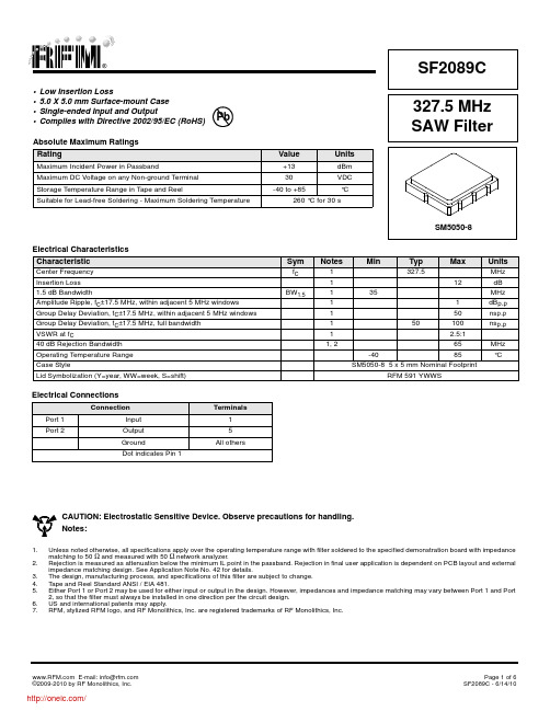
1.Unless noted otherwise, all specifications apply over the operating temperature range with filter soldered to the specified demonstration board with impedance matching to 50 Ω and measured with 50 Ω network analyzer.2.Rejection is measured as attenuation below the minimum IL point in the passband. Rejection in final user application is dependent on PCB layout and external impedance matching design. See Application Note No. 42 for details.3.The design, manufacturing process, and specifications of this filter are subject to change.4.Tape and Reel Standard ANSI / EIA 481.5.Either Port 1 or Port 2 may be used for either input or output in the design. However, impedances and impedance matching may vary between Port 1 and Port 2, so that the filter must always be installed in one direction per the circuit design. and international patents may apply.7.RFM, stylized RFM logo, and RF Monolithics, Inc. are registered trademarks of RF Monolithics, Inc.Electrical Characteristics CharacteristicSymNotesMin TypMaxUnitsCenter Frequency f C 1327.5MHz Insertion Loss 112dB 1.5 dB BandwidthBW 1.5135MHz Amplitude Ripple, f C ±17.5 MHz, within adjacent 5 MHz windows11dB P-P Group Delay Deviation, f C ±17.5 MHz, within adjacent 5 MHz windows 150ns P-P Group Delay Deviation, f C ±17.5 MHz, full bandwidth 150100ns P-P VSWR at f C1 2.5:1 40 dB Rejection Bandwidth 1, 265MHz Operating Temperature Range -4085°CCase StyleSM5050-8 5 x 5 mm Nominal FootprintLid Symbolization (Y=year, WW=week, S=shift)RFM 591 YWWSSM5050-8•Low Insertion Loss•5.0 X 5.0 mm Surface-mount Case •Single-ended Input and Output•Complies with Directive 2002/95/EC (RoHS)Absolute Maximum Ratings RatingValueUnitsMaximum Incident Power in Passband+13dBm Maximum DC Voltage on any Non-ground Terminal 30VDC Storage Temperature Range in Tape and Reel-40 to +85°CSuitable for Lead-free Soldering - Maximum Soldering Temperature260 °C for 30 s327.5 MHz SAW FilterSF2089CPbCAUTION: Electrostatic Sensitive Device. Observe precautions for handling.Notes:Electrical ConnectionsConnectionTerminalsPort 1Input 1Port 2Output 5GroundAll othersDot indicates Pin 1Case DimensionsDimensionmm Inches Min Nom Max Min Nom Max A 4.80 5.00 5.200.1890.1970.205B 4.80 5.00 5.200.1890.1970.205C 1.30 1.50 1.700.0500.0600.067D 1.98 2.08 2.180.0780.0820.086E 1.07 1.17 1.270.0420.0460.050F 0.500.640.700.0200.0250.028G 2.392.54 2.690.0940.1000.106H 1.270.050I 0.760.030J 1.550.061K 2.790.110L 0.760.030M 2.360.093N 1.550.061O 2.790.110P 2.790.110Q2.790.110MaterialsSolder Pad Plating 0.3 to 1.0 µm Gold over 1.27 to 8.89 µm NickelLid Plating 2.0 to 3.0 µm Nickel BodyAl 2O 3 CeramicPb FreeSM5050-8 Surface-Mount 8-Terminal Ceramic Case5.0 X 5.0 mm Nominal FootprintTOP VIEW BOTTOM VIEWCase MaterialsTape and Reel Specifications“B”Nominal Size Quantity Per ReelInches millimeters7178500133303000USER DIRECTION OF FEEDCOMPONENT ORIENTATION and DIMENSIONSCarrier Tape DimensionsAo 5.3 mm Bo 5.3 mm Ko 2.0 mm Pitch 8.0 mm W 12.0 mmPIN #1分销商库存信息: RFMSF2089C。

深圳国芯人工智能有限公司STC8H 系列单片机技术参考手册技术支持网站:官方技术论坛:资料更新日期:2023/9/12 (本文档可直接添加备注和标记)目录1单片机基础概述 (1)1.1 数制与编码 (1)1.1.1 数制转换 (1)1.1.2 原码、反码及补码 (4)1.1.3 常用编码 (5)1.2 几种常用的逻辑运算及其图形符号 (5)1.3 STC8H单片机性能概述 (9)1.4 STC8H单片机产品线 (10)2特性、价格及管脚 (11)2.1 STC8H1K08-36I-TSSOP20/QFN20,SOP20/16系列 (11)2.1.1 特性及价格 (11)2.1.2 管脚图,最小系统 (14)2.1.3 管脚说明 (17)2.2 STC8H1K28-36I-LQFP/QFN32,TSSOP/SOP28,TSSOP20系列 (20)2.2.1 特性及价格 (20)2.2.2 管脚图,最小系统 (23)2.2.3 管脚说明 (26)2.3 STC8H3K64S2-40I-LQFP48/32,QFN48/32,TSSOP20系列 (30)2.3.1 特性及价格(有16位硬件乘除法器MDU16,准16位单片机) (30)2.3.2 管脚图,最小系统 (33)2.3.3 管脚说明 (37)2.4 STC8H3K64S4-40I-LQFP48/32,QFN48/32,TSSOP20系列 (43)2.4.1 特性及价格(有16位硬件乘除法器MDU16,准16位单片机) (43)2.4.2 管脚图,最小系统 (46)2.4.3 管脚说明 (49)2.5 STC8H8K64U-LQFP/QFN-64/48/32,TSSOP20,SKDIP28,PDIP40 (55)2.5.1 特性及价格(有16位硬件乘除法器MDU16,准16位单片机) (55)2.5.2 STC8H8K64U系列内部结构图 (58)2.5.3 管脚图,最小系统 (59)2.5.4 管脚说明 (73)2.6 STC8H4K64TL-40I-LQFP48/32、QFN48、TSSOP20 (79)2.6.1 特性及价格(有16位硬件乘除法器MDU16,准16位单片机) (79)2.6.2 管脚图,最小系统 (82)2.6.3 RTC实战线路图 (85)2.6.4 管脚说明 (86)2.7 STC8H4K64TLCD-40I-LQFP64/48、QFN64/48 (93)2.7.1 特性及价格(有16位硬件乘除法器MDU16,准16位单片机) (93)2.7.2 管脚图,最小系统 (96)2.7.3 RTC实战线路图 (98)2.7.4 管脚说明 (99)2.8 STC8H1K08T-33I-TSSOP20/QFN20/SOP16 (108)2.8.1 特性及价格(有16位硬件乘除法器MDU16,准16位单片机) (108)2.8.2 管脚图,最小系统 (111)2.8.3 管脚说明 (114)2.9 STC8H2K08U-TSSOP20,QFN20,SOP16(提前预告) (118)2.9.1 特性及价格(有16位硬件乘除法器MDU16,准16位单片机) (118)2.9.2 管脚图,最小系统 (121)2.9.3 管脚说明 (127)2.10 STC8051H-42I-LQFP48/44、PDIP40 (131)2.10.1 特性及价格 (131)2.10.2 管脚图,最小系统 (134)3功能脚切换 (137)3.1 功能脚切换相关寄存器 (137)3.1.1 外设端口切换控制寄存器1(P_SW1),串口1、SPI切换 (137)3.1.2 外设端口切换控制寄存器2(P_SW2),串口2/3/4、I2C、比较器输出切换 (138)3.1.3 时钟选择寄存器(MCLKOCR) (138)3.1.4 T3/T4选择寄存器(T3T4PIN) (138)3.1.5 高级PWM选择寄存器(PWMx_PS) (140)3.1.6 高级PWM功能脚选择寄存器(PWMx_ETRPS) (142)3.2 范例程序 (143)3.2.1 串口1切换 (143)3.2.2 串口2切换 (144)3.2.3 串口3切换 (145)3.2.4 串口4切换 (147)3.2.5 SPI切换 (148)3.2.6 I2C切换 (150)3.2.7 比较器输出切换 (151)3.2.8 主时钟输出切换 (152)4封装尺寸图 (155)4.1 SOP8封装尺寸图 (155)4.2 DFN8封装尺寸图(3mm*3mm) (156)4.3 SOP16封装尺寸图 (157)4.4 SOP20封装尺寸图 (158)4.5 TSSOP20封装尺寸图 (159)4.6 QFN20封装尺寸图(3mm*3mm) (160)4.7 SOP28封装尺寸图 (161)4.8 TSSOP28封装尺寸图 (162)4.9 LQFP32封装尺寸图(9mm*9mm) (163)4.10 QFN32封装尺寸图(4mm*4mm) (164)4.11 LQFP48封装尺寸图(9mm*9mm) (165)4.12 QFN48封装尺寸图(6mm*6mm) (166)4.13 LQFP64封装尺寸图(12mm*12mm) (167)4.14 QFN64封装尺寸图(8mm*8mm) (168)4.15 STC8H系列单片机命名规则 (169)5ISP下载流程及典型应用线路图 (170)5.1.1 ISP下载流程图(串口下载模式) (170)5.1.2 ISP下载流程图(硬件/软件模拟USB+串口模式) (171)5.2 STC8H系列ISP下载应用线路图 (172)5.2.1 使用STC-USB Link1D工具下载,支持在线和脱机下载 (172)5.2.2 硬件USB直接ISP下载(5V系统) (174)5.2.3 硬件USB直接ISP下载(3.3V系统) (176)5.2.4 软件模拟硬件USB直接ISP下载,建议尝试,不支持仿真(5V系统) (177)5.2.5 软件模拟硬件USB直接ISP下载,建议尝试,不支持仿真(3.3V系统) (179)5.2.6 使用一箭双雕之USB转串口工具下载 (181)5.2.7 使用USB转双串口/TTL下载(有外部晶振) (183)5.2.8 使用USB转双串口/TTL下载(无外部晶振) (184)5.2.9 使用USB转双串口/TTL下载(自动停电/上电) (186)5.2.10 使用USB转双串口/RS485下载(5.0V) (187)5.2.11 使用USB转双串口/RS485下载(3.3V) (187)5.2.12 使用USB转双串口/RS232下载(5.0V) (189)5.2.13 使用USB转双串口/RS232下载(3.3V) (189)5.2.14 使用U8-Mini工具下载,支持ISP在线和脱机下载,也可支持仿真 (190)5.2.15 使用U8W工具下载,支持ISP在线和脱机下载,也可支持仿真 (192)5.2.16 使用RS-232转换器下载,也可支持仿真 (194)5.2.17 使用PL2303-GL下载,也可支持仿真 (195)5.2.18 单片机电源控制参考电路 (197)5.3 用STC一箭双雕之USB转双串口仿真STC8系列MCU (198)5.4 STC-ISP下载软件高级应用 (207)5.4.1 发布项目程序 (207)5.4.2 程序加密后传输(防烧录时串口分析出程序) (213)5.4.3 发布项目程序+程序加密后传输结合使用 (218)5.4.4 用户自定义下载(实现不停电下载) (220)5.4.5 如何简单的控制下载次数,通过ID号来限制实际可以下载的MCU数量 (224)6时钟、复位、看门狗与电源管理 (228)6.1 系统时钟控制 (228)6.1.1 系统时钟选择寄存器(CLKSEL) (230)6.1.2 时钟分频寄存器(CLKDIV) (230)6.1.3 内部高速高精度IRC控制寄存器(HIRCCR) (231)6.1.4 外部振荡器控制寄存器(XOSCCR) (231)6.1.5 外部32K振荡器控制寄存器(X32KCR) (232)6.1.6 内部低速IRC控制寄存器(IRC32KCR) (233)6.1.7 主时钟输出控制寄存器(MCLKOCR) (234)6.1.8 高速振荡器稳定时间控制寄存器(IRCDB) (234)6.1.9 USB时钟控制寄存器(USBCLK) (234)6.1.10 PLL时钟控制寄存器(PLLCR) (235)6.2 STC8H系列内部IRC频率调整 (236)6.2.1 IRC频段选择寄存器(IRCBAND) (237)6.2.2 内部IRC频率调整寄存器(IRTRIM) (237)6.2.3 内部IRC频率微调寄存器(LIRTRIM) (239)6.2.4 时钟分频寄存器(CLKDIV) (239)6.2.5 分频出3MHz用户工作频率,并用户动态改变频率追频示例 (240)6.3 系统复位 (243)6.3.1 看门狗复位(WDT_CONTR) (244)6.3.2 软件复位(IAP_CONTR) (246)6.3.3 低压复位(RSTCFG) (247)6.3.4 复位标志寄存器(RSTFLAG) (247)6.3.5 低电平上电复位参考电路(一般不需要) (249)6.3.6 低电平按键复位参考电路 (249)6.3.7 传统8051高电平上电复位参考电路 (250)6.4 外部晶振及外部时钟电路 (251)6.4.1 外部晶振输入电路 (251)6.4.2 外部时钟输入电路(P1.6为高阻输入模式,可当输入口使用) (251)6.5 时钟停振/省电模式与系统电源管理 (252)6.5.1 电源控制寄存器(PCON) (252)6.6 掉电唤醒定时器 (253)6.6.1 掉电唤醒定时器计数寄存器(WKTCL,WKTCH) (253)6.7 范例程序 (254)6.7.1 选择系统时钟源 (254)6.7.2 主时钟分频输出 (256)6.7.3 看门狗定时器应用 (257)6.7.4 软复位实现自定义下载 (259)6.7.5 低压检测 (261)6.7.6 省电模式 (262)6.7.7 使用INT0/INT1/INT2/INT3/INT4管脚中断唤醒省电模式 (264)6.7.8 使用T0/T1/T2/T3/T4管脚中断唤醒省电模式 (267)6.7.9 使用RxD/RxD2/RxD3/RxD4管脚中断唤醒省电模式 (271)6.7.10 使用I2C的SDA脚唤醒MCU省电模式 (274)6.7.11 使用掉电唤醒定时器唤醒省电模式 (276)6.7.12 LVD中断唤醒省电模式,建议配合使用掉电唤醒定时器 (278)6.7.13 比较器中断唤醒省电模式,建议配合使用掉电唤醒定时器 (281)6.7.14 使用LVD功能检测工作电压(电池电压) (283)7自动频率校准,自动追频(CRE) (288)7.1 相关寄存器 (288)7.1.1 CRE控制寄存器(CRECR) (288)7.1.2 CRE校准计数值寄存器(CRECNT) (289)7.1.3 CRE校准误差值寄存器(CRERES) (289)7.2 范例程序 (290)7.2.1 自动校准内部高速IRC(HIRC) (290)8存储器 (292)8.1 程序存储器 (292)8.2 数据存储器 (293)8.2.1 内部RAM (293)8.2.3 内部扩展RAM,XRAM,XDATA (295)8.2.4 辅助寄存器(AUXR) (295)8.2.5 外部扩展RAM,XRAM,XDATA (296)8.2.6 总线速度控制寄存器(BUS_SPEED) (296)8.2.7 8051中可位寻址的数据存储器 (297)8.2.8 扩展SFR使能寄存器EAXFR的使用说明 (299)8.3 存储器中的特殊参数,在ISP下载时可烧录进程序FLASH (300)8.4 只读特殊功能寄存器中存储的唯一ID号和重要参数(CHIPID) (305)8.4.1 CHIP之全球唯一ID号解读 (307)8.4.2 CHIP之内部参考信号源解读 (307)8.4.3 CHIP之内部32K的IRC振荡频率解读 (308)8.4.4 CHIP之高精度IRC参数解读 (309)8.4.5 CHIP之测试时间参数解读 (310)8.4.6 CHIP之芯片封装形式编号解读 (310)8.5 范例程序 (311)8.5.1 ) (311)8.5.2 ROM)中读取) (314)8.5.38.5.48.5.5 ) (322)8.5.68.5.78.5.8 ROM)中读取) (331)8.5.98.5.108.5.11 ROM)中读取) (344)8.5.12 ROM)中读取) (349)8.5.13 用户自定义内部IRC频率(从RAM中读取)9特殊功能寄存器 (358)9.1 STC8H1K08系列 (358)9.2 STC8H1K28系列 (360)9.3 STC8H3K64S4系列 (361)9.4 STC8H3K64S2系列 (363)9.5 STC8H8K64U-64Pin/48Pin USB系列 (365)9.6 STC8H4K64TL系列 (367)9.7 STC8H4K64TLCD系列 (369)9.8 STC8H1K08T系列 (371)9.9 STC8H2K08U系列 (373)9.10 特殊功能寄存器列表 (375)10I/O口 (389)10.1 I/O口相关寄存器 (389)10.1.1 端口数据寄存器(Px) (392)10.1.2 端口模式配置寄存器(PxM0,PxM1) (392)10.1.4 端口施密特触发控制寄存器(PxNCS) (393)10.1.5 端口电平转换速度控制寄存器(PxSR) (394)10.1.6 端口驱动电流控制寄存器(PxDR) (394)10.1.7 端口数字信号输入使能控制寄存器(PxIE) (394)10.2 配置I/O口 (396)10.3 I/O的结构图 (397)10.3.1 准双向口(弱上拉) (397)10.3.2 推挽输出 (397)10.3.3 高阻输入 (398)10.3.4 开漏输出 (398)10.3.5 新增4.1K上拉电阻 (399)10.3.6 如何设置I/O口对外输出速度 (399)10.3.7 如何设置I/O口电流驱动能力 (400)10.3.8 如何降低I/O口对外辐射 (400)10.4 STC-ISP | I/O口配置工具 (401)10.4.1 普通配置模式 (401)10.4.2 高级配置模式 (402)10.5 范例程序 (403)10.5.1 端口模式设置 (403)10.5.2 双向口读写操作 (404)10.6 一种典型三极管控制电路 (407)10.7 典型发光二极管控制电路 (408)10.8 混合电压供电系统3V/5V器件I/O口互连 (408)10.9 如何让I/O口上电复位时为低电平 (409)10.10 利用74HC595驱动8个数码管(串行扩展,3根线)的线路图 (410)10.11 I/O口直接驱动LED数码管应用线路图 (411)10.12 用STC系列MCU的I/O口直接驱动段码LCD (412)10.13 使用I/O和R-2R电阻分压实现DAC的经典线路图 (431)11指令系统 (432)11.1 寻址方式 (432)11.1.1 立即寻址 (432)11.1.2 直接寻址 (432)11.1.3 间接寻址 (432)11.1.4 寄存器寻址 (432)11.1.5 相对寻址 (432)11.1.6 变址寻址 (433)11.1.7 位寻址 (433)11.2 指令表 (433)11.3 指令详解(中文) (436)11.4 指令详解(英文) (469)11.5 多级流水线内核的中断响应 (504)12中断系统 (506)12.1 STC8H系列中断源 (506)12.3 STC8H系列中断列表 (510)12.4 中断相关寄存器 (513)12.4.1 中断使能寄存器(中断允许位) (515)12.4.2 中断请求寄存器(中断标志位) (520)12.4.3 中断优先级寄存器 (524)12.5 范例程序 (531)12.5.1 INT0中断(上升沿和下降沿),可同时支持上升沿和下降沿 (531)12.5.2 INT0中断(下降沿) (532)12.5.3 INT1中断(上升沿和下降沿),可同时支持上升沿和下降沿 (534)12.5.4 INT1中断(下降沿) (536)12.5.5 INT2中断(下降沿),只支持下降沿中断 (537)12.5.6 INT3中断(下降沿),只支持下降沿中断 (539)12.5.7 INT4中断(下降沿),只支持下降沿中断 (541)12.5.8 定时器0中断 (542)12.5.9 定时器1中断 (544)12.5.10 定时器2中断 (546)12.5.11 定时器3中断 (548)12.5.12 定时器4中断 (549)12.5.13 UART1中断 (551)12.5.14 UART2中断 (553)12.5.15 UART3中断 (556)12.5.16 UART4中断 (558)12.5.17 ADC中断 (560)12.5.18 LVD中断 (562)12.5.19 比较器中断 (564)12.5.20 SPI中断 (566)12.5.21 I2C中断 (567)13所有的I/O口均可中断(4种模式),不是传统外部中断 (570)13.1 I/O口中断相关寄存器 (570)13.1.1 端口中断使能寄存器(PxINTE) (571)13.1.2 端口中断标志寄存器(PxINTF) (572)13.1.3 端口中断模式配置寄存器(PxIM0,PxIM1) (572)13.1.4 端口中断优先级控制寄存器(PINIPL,PINIPH) (573)13.1.5 端口中断掉电唤醒使能寄存器(PxWKUE) (573)13.2 范例程序 (575)13.2.1 P0口下降沿中断 (575)13.2.2 P1口上升沿中断 (578)13.2.3 P2口低电平中断 (581)13.2.4 P3口高电平中断 (585)13.2.5 使用拓展Keil中断号方案的I/O口中断范例 (588)14定时器/计数器 (591)14.1 定时器3/4功能脚切换 (591)14.2 定时器的相关寄存器 (592)14.3.1 定时器0/1控制寄存器(TCON) (593)14.3.2 定时器0/1模式寄存器(TMOD) (593)14.3.3 定时器0模式0(16位自动重装载模式) (594)14.3.4 定时器0模式1(16位不可重装载模式) (595)14.3.5 定时器0模式2(8位自动重装载模式) (596)14.3.6 定时器0模式3(不可屏蔽中断16位自动重装载,实时操作系统节拍器) (596)14.3.7 定时器1模式0(16位自动重装载模式) (597)14.3.8 定时器1模式1(16位不可重装载模式) (598)14.3.9 定时器1模式2(8位自动重装载模式) (599)14.3.10 定时器0计数寄存器(TL0,TH0) (599)14.3.11 定时器1计数寄存器(TL1,TH1) (599)14.3.12 辅助寄存器1(AUXR) (599)14.3.13 中断与时钟输出控制寄存器(INTCLKO) (600)14.3.14 定时器0计算公式 (600)14.3.15 定时器1计算公式 (601)14.4 定时器2(24位定时器,8位预分频+16位定时) (602)14.4.1 辅助寄存器1(AUXR) (602)14.4.2 中断与时钟输出控制寄存器(INTCLKO) (602)14.4.3 定时器2计数寄存器(T2L,T2H) (602)14.4.4 定时器2的8位预分频寄存器(TM2PS) (602)14.4.5 定时器2工作模式 (603)14.4.6 定时器2计算公式 (603)14.5 定时器3/4(24位定时器,8位预分频+16位定时) (604)14.5.1 定时器4/3控制寄存器(T4T3M) (604)14.5.2 定时器3计数寄存器(T3L,T3H) (604)14.5.3 定时器4计数寄存器(T4L,T4H) (604)14.5.4 定时器3的8位预分频寄存器(TM3PS) (605)14.5.5 定时器4的8位预分频寄存器(TM4PS) (605)14.5.6 定时器3工作模式 (605)14.5.7 定时器4工作模式 (607)14.5.8 定时器3计算公式 (607)14.5.9 定时器4计算公式 (608)14.6 定时器T11(24位定时器,8位预分频+16位定时) (609)14.6.1 定时器T11控制寄存器(T11CR) (609)14.6.2 定时器T11的8位预分频寄存器(T11PS) (609)14.6.3 定时器T11计数寄存器(T11L,T11H) (609)14.6.4 定时器T11工作模式 (610)14.6.5 定时器T11计算公式 (611)14.7 STC-ISP | 定时器计算器工具 (612)14.8 范例程序 (613)14.8.1 定时器0(模式0-16位自动重载),用作定时 (613)14.8.2 定时器0(模式1-16位不自动重载),用作定时 (614)14.8.3 定时器0(模式2-8位自动重载),用作定时 (616)14.8.4 定时器0(模式3-16位自动重载不可屏蔽中断),用作定时 (618)14.8.5 定时器0(外部计数-扩展T0为外部下降沿中断) (620)14.8.6 定时器0(测量脉宽-INT0高电平宽度) (621)14.8.7 定时器0(模式0),时钟分频输出 (623)14.8.8 定时器1(模式0-16位自动重载),用作定时 (625)14.8.9 定时器1(模式1-16位不自动重载),用作定时 (626)14.8.10 定时器1(模式2-8位自动重载),用作定时 (628)14.8.11 定时器1(外部计数-扩展T1为外部下降沿中断) (630)14.8.12 定时器1(测量脉宽-INT1高电平宽度) (632)14.8.13 定时器1(模式0),时钟分频输出 (634)14.8.14 定时器1(模式0)做串口1波特率发生器 (635)14.8.15 定时器1(模式2)做串口1波特率发生器 (639)14.8.16 定时器2(16位自动重载),用作定时 (643)14.8.17 定时器2(外部计数-扩展T2为外部下降沿中断) (644)14.8.18 定时器2,时钟分频输出 (646)14.8.19 定时器2做串口1波特率发生器 (648)14.8.20 定时器2做串口2波特率发生器 (651)14.8.21 定时器2做串口3波特率发生器 (655)14.8.22 定时器2做串口4波特率发生器 (659)14.8.23 定时器3(16位自动重载),用作定时 (663)14.8.24 定时器3(外部计数-扩展T3为外部下降沿中断) (665)14.8.25 定时器3,时钟分频输出 (667)14.8.26 定时器3做串口3波特率发生器 (668)14.8.27 定时器4(16位自动重载),用作定时 (672)14.8.28 定时器4(外部计数-扩展T4为外部下降沿中断) (674)14.8.29 定时器4,时钟分频输出 (676)14.8.30 定时器4做串口4波特率发生器 (678)15超级简单的STC USB-CDC虚拟串口应用 (682)15.1 USB-CDC虚拟串口概述 (682)15.2 新建Keil项目并加入CDC模块 (683)15.3 USB-CDC虚拟串口与电脑进行数据传输 (690)15.4 STC USB-CDC虚拟串口实现不停电自动ISP下载 (691)16串口通信 (692)16.1 串口功能脚切换 (692)16.2 串口相关寄存器 (693)16.3 串口1 (694)16.3.1 串口1控制寄存器(SCON) (694)16.3.2 串口1数据寄存器(SBUF) (694)16.3.3 电源管理寄存器(PCON) (695)16.3.4 辅助寄存器1(AUXR) (695)16.3.5 串口1模式0,模式0波特率计算公式 (695)16.3.6 串口1模式1,模式1波特率计算公式 (696)16.3.7 串口1模式2,模式2波特率计算公式 (699)16.3.8 串口1模式3,模式3波特率计算公式 (699)16.3.9 自动地址识别 (700)16.3.10 串口1从机地址控制寄存器(SADDR,SADEN) (700)16.4 串口2 (702)16.4.1 串口2控制寄存器(S2CON) (702)16.4.2 串口2数据寄存器(S2BUF) (702)16.4.3 串口2模式0,模式0波特率计算公式 (702)16.4.4 串口2模式1,模式1波特率计算公式 (703)16.5 串口3 (705)16.5.1 串口3控制寄存器(S3CON) (705)16.5.2 串口3数据寄存器(S3BUF) (705)16.5.3 串口3模式0,模式0波特率计算公式 (705)16.5.4 串口3模式1,模式1波特率计算公式 (706)16.6 串口4 (708)16.6.1 串口4控制寄存器(S4CON) (708)16.6.2 串口4数据寄存器(S4BUF) (708)16.6.3 串口4模式0,模式0波特率计算公式 (708)16.6.4 串口4模式1,模式1波特率计算公式 (709)16.7 串口注意事项 (711)16.8 STC-ISP | 串口波特率计算器工具 (712)16.9 STC-ISP | 串口助手/USB-CDC (713)16.10 范例程序 (717)16.10.1 串口1使用定时器2做波特率发生器 (717)16.10.2 串口1使用定时器1(模式0)做波特率发生器 (720)16.10.3 串口1使用定时器1(模式2)做波特率发生器 (724)16.10.4 串口2使用定时器2做波特率发生器 (728)16.10.5 串口3使用定时器2做波特率发生器 (732)16.10.6 串口3使用定时器3做波特率发生器 (735)16.10.7 串口4使用定时器2做波特率发生器 (739)16.10.8 串口4使用定时器4做波特率发生器 (743)16.10.9 串口多机通讯 (748)16.10.10 串口中断收发-MODBUS协议 (749)16.10.11 串口转LIN总线 (760)17比较器,掉电检测,内部1.19V参考信号源(BGV) (768)17.1 比较器内部结构图 (769)17.2 比较器输出功能脚切换 (769)17.3 比较器相关的寄存器 (770)17.3.1 比较器控制寄存器1(CMPCR1) (770)17.3.2 比较器控制寄存器2(CMPCR2) (771)17.3.3 比较器扩展配置寄存器(CMPEXCFG) (771)17.4 范例程序 (773)17.4.1 旧版比较器的使用(中断方式) (773)17.4.2 旧版比较器的使用(查询方式) (775)17.4.3 新版比较器的使用(中断方式) (777)17.4.4 新版比较器的使用(查询方式) (780)17.4.5 旧版比较器的多路复用应用(比较器+ADC输入通道) (783)17.4.6 新版比较器的多路复用应用(比较器+ADC输入通道) (784)17.4.7 比较器作外部掉电检测(掉电过程中应及时保存用户数据到EEPROM中) (787)17.4.8 比较器检测工作电压(电池电压) (788)18IAP/EEPROM/DATA-FLASH (792)18.1 EEPROM操作时间 (792)18.2 EEPROM相关的寄存器 (792)18.2.1 EEPROM数据寄存器(IAP_DATA) (792)18.2.2 EEPROM地址寄存器(IAP_ADDR) (793)18.2.3 EEPROM命令寄存器(IAP_CMD) (793)18.2.4 EEPROM触发寄存器(IAP_TRIG) (793)18.2.5 EEPROM控制寄存器(IAP_CONTR) (793)18.2.6 EEPROM等待时间控制寄存器(IAP_TPS) (794)18.3 EEPROM大小及地址 (795)18.4 范例程序 (798)18.4.1 EEPROM基本操作 (798)18.4.2 使用MOVC读取EEPROM (801)18.4.3 使用串口送出EEPROM数据 (804)18.4.4 串口1读写EEPROM-带MOVC读 (808)18.4.5 口令擦除写入-多扇区备份-串口1操作 (815)19ADC模数转换,内部1.19V参考信号源(BGV) (825)19.1 ADC相关的寄存器 (825)19.1.1 ADC控制寄存器(ADC_CONTR),PWM触发ADC控制 (826)19.1.2 ADC配置寄存器(ADCCFG) (828)19.1.3 ADC转换结果寄存器(ADC_RES,ADC_RESL) (829)19.1.4 ADC时序控制寄存器(ADCTIM) (830)19.1.5 ADC扩展配置寄存器(ADCEXCFG) (831)19.2 ADC相关计算公式 (832)19.2.1 ADC速度计算公式 (832)19.2.2 ADC转换结果计算公式 (832)19.2.3 反推ADC输入电压计算公式 (832)19.2.4 反推工作电压计算公式 (834)19.3 10位ADC静态特性 (834)19.4 12位ADC静态特性 (834)19.5 ADC应用参考线路图 (835)19.5.1 一般精度ADC参考线路图 (835)19.5.2 高精度ADC参考线路图 (836)19.5.3 高精度ADC参考线路图(有独立A Vcc和AGnd) (837)19.6 STC-ISP | ADC转换速度计算器工具 (838)19.7 范例程序 (839)19.7.1 ADC基本操作(查询方式) (839)19.7.2 ADC基本操作(中断方式) (841)19.7.3 格式化ADC转换结果 (843)19.7.4 利用ADC第15通道测量外部电压或电池电压 (845)19.7.5 ADC作按键扫描应用线路图 (848)19.7.6 检测负电压参考线路图 (849)19.7.7 常用加法电路在ADC中的应用 (850)20同步串行外设接口SPI (851)20.1 SPI功能脚切换 (851)20.2 SPI相关的寄存器 (851)20.2.1 SPI状态寄存器(SPSTAT) (851)20.2.2 SPI控制寄存器(SPCTL),SPI速度控制 (852)20.2.3 SPI数据寄存器(SPDAT) (853)20.3 SPI通信方式 (854)20.3.1 单主单从 (854)20.3.2 互为主从 (854)20.3.3 单主多从 (855)20.4 配置SPI (856)20.5 数据模式 (858)20.6 范例程序 (859)20.6.1 SPI单主单从系统主机程序(中断方式) (859)20.6.2 SPI单主单从系统从机程序(中断方式) (861)20.6.3 SPI单主单从系统主机程序(查询方式) (863)20.6.4 SPI单主单从系统从机程序(查询方式) (865)20.6.5 SPI互为主从系统程序(中断方式) (867)20.6.6 SPI互为主从系统程序(查询方式) (869)21I2C总线 (873)21.1 I2C功能脚切换 (873)21.2 I2C相关的寄存器 (873)21.3 I2C主机模式 (875)21.3.1 I2C配置寄存器(I2CCFG),总线速度控制 (875)21.3.2 I2C主机控制寄存器(I2CMSCR) (876)21.3.3 I2C主机辅助控制寄存器(I2CMSAUX) (877)21.3.4 I2C主机状态寄存器(I2CMSST) (877)21.4 I2C从机模式 (879)21.4.1 I2C从机控制寄存器(I2CSLCR) (879)21.4.2 I2C从机状态寄存器(I2CSLST) (879)21.4.3 I2C从机地址寄存器(I2CSLADR) (881)21.4.4 I2C数据寄存器(I2CTXD,I2CRXD) (882)21.5 范例程序 (883)21.5.1 I2C主机模式访问AT24C256(中断方式) (883)21.5.2 I2C主机模式访问AT24C256(查询方式) (888)21.5.3 I2C主机模式访问PCF8563 (894)21.5.4 I2C从机模式(中断方式) (899)21.5.5 I2C从机模式(查询方式) (903)21.5.6 测试I2C从机模式代码的主机代码 (907)2216位高级PWM定时器,支持正交编码器 (913)22.1 简介 (916)22.2 主要特性 (916)22.3 时基单元 (919)22.3.1 读写16位计数器 (919)22.3.2 16位PWMA_ARR寄存器的写操作 (920)22.3.3 预分频器 (920)22.3.4 向上计数模式 (920)22.3.5 向下计数模式 (921)22.3.6 中间对齐模式(向上/向下计数) (923)22.3.7 重复计数器 (924)22.4 时钟/触发控制器 (925)22.4.1 预分频时钟(CK_PSC) (925)22.4.2 内部时钟源(f MASTER) (925)22.4.3 外部时钟源模式1 (926)22.4.4 外部时钟源模式2 (926)22.4.5 触发同步 (927)22.4.6 与PWMB同步 (929)22.5 捕获/比较通道 (932)22.5.1 16位PWMA_CCRi寄存器的写流程 (933)22.5.2 输入模块 (933)22.5.3 输入捕获模式 (934)22.5.4 输出模块 (935)22.5.5 强制输出模式 (936)22.5.6 输出比较模式 (936)22.5.7 PWM模式 (937)22.5.8 使用刹车功能(PWMFLT) (942)22.5.9 在外部事件发生时清除OCiREF信号 (943)22.5.10 编码器接口模式 (944)22.6 中断 (945)22.7 PWMA/PWMB寄存器描述 (947)22.7.1 高级PWM功能脚切换 (947)22.7.2 输出使能寄存器(PWMx_ENO) (948)22.7.3 输出附加使能寄存器(PWMx_IOAUX) (949)22.7.4 控制寄存器1(PWMx_CR1) (950)22.7.5 控制寄存器2(PWMx_CR2),及实时触发ADC (951)22.7.6 从模式控制寄存器(PWMx_SMCR) (953)22.7.7 外部触发寄存器(PWMx_ETR) (955)22.7.8 中断使能寄存器(PWMx_IER) (955)22.7.9 状态寄存器1(PWMx_SR1) (956)22.7.10 状态寄存器2(PWMx_SR2) (957)22.7.11 事件产生寄存器(PWMx_EGR) (957)22.7.12 捕获/比较模式寄存器1(PWMx_CCMR1) (958)22.7.13 捕获/比较模式寄存器2(PWMx_CCMR2) (961)22.7.14 捕获/比较模式寄存器3(PWMx_CCMR3) (962)22.7.15 捕获/比较模式寄存器4(PWMx_CCMR4) (963)22.7.16 捕获/比较使能寄存器1(PWMx_CCER1) (964)22.7.17 捕获/比较使能寄存器2(PWMx_CCER2) (966)22.7.18 计数器高8位(PWMx_CNTRH) (966)22.7.19 计数器低8位(PWMx_CNTRL) (967)22.7.20 预分频器高8位(PWMx_PSCRH),输出频率计算公式 (967)22.7.21 预分频器低8位(PWMx_PSCRL) (967)22.7.22 自动重装载寄存器高8位(PWMx_ARRH) (967)22.7.23 自动重装载寄存器低8位(PWMx_ARRL) (968)22.7.24 重复计数器寄存器(PWMx_RCR) (968)22.7.25 捕获/比较寄存器1/5高8位(PWMx_CCR1H) (968)22.7.26 捕获/比较寄存器1/5低8位(PWMx_CCR1L) (968)22.7.27 捕获/比较寄存器2/6高8位(PWMx_CCR2H) (969)22.7.28 捕获/比较寄存器2/6低8位(PWMx_CCR2L) (969)22.7.29 捕获/比较寄存器3/7高8位(PWMx_CCR3H) (969)22.7.30 捕获/比较寄存器3/7低8位(PWMx_CCR3L) (969)22.7.31 捕获/比较寄存器4/8高8位(PWMx_CCR4H) (969)22.7.32 捕获/比较寄存器4/8低8位(PWMx_CCR4L) (969)22.7.33 刹车寄存器(PWMx_BKR) (969)22.7.34 死区寄存器(PWMx_DTR) (970)22.7.35 输出空闲状态寄存器(PWMx_OISR) (971)22.8 范例程序 (972)22.8.1 BLDC无刷直流电机驱动(带HALL) (972)22.8.2 BLDC无刷直流电机驱动(无HALL),一个比较器当3个比较器分时复用 (981)22.8.3 使用高级PWM实现编码器 (988)22.8.4 正交编码器模式 (991)22.8.5 单脉冲模式(触发控制脉冲输出) (992)22.8.6 门控模式(输入电平使能计数器) (993)22.8.7 外部时钟模式 (995)22.8.8 输入捕获模式测量脉冲周期(捕获上升沿到上升沿或者下降沿到下降沿) (997)22.8.9 输入捕获模式测量脉冲高电平宽度(捕获上升沿到下降沿) (999)22.8.10 输入捕获模式测量脉冲低电平宽度(捕获下降沿到上升沿) (1001)22.8.11 输入捕获模式同时测量脉冲周期和高电平宽度(占空比) (1003)22.8.12 同时捕获4路输入信号的周期和高电平宽度(占空比) (1005)22.8.13 输出占空比为100%和0%的PWM波形的方法(以PWM1P为例) (1011)22.8.14 带死区控制的PWM互补输出 (1012)22.8.15 PWM端口做外部中断(下降沿中断或者上升沿中断) (1013)22.8.16 输出任意周期和任意占空比的波形 (1014)22.8.17 使用PWM的CEN启动PWMA定时器,实时触发ADC (1014)22.8.18 PWM周期重复触发ADC (1015)22.8.19 利用PWM实现16位DAC的参考线路图 (1016)22.8.20 利用PWM实现互补SPWM (1016)22.8.21 高级PWM输出-频率可调-脉冲计数(软件方式) (1020)22.8.22 高级PWM输出-频率可调-脉冲计数(硬件方式) (1023)22.8.23 产生3路相位差120度的互补PWM波形(网友提供) (1027)22.8.24 高级PWM时钟输出应用(系统时钟2分频输出) (1028)22.8.25 输出两路有相位差的PWM(PWMA) (1029)22.8.26 输出两路有相位差的PWM(PWMB) (1031)22.8.27 PWMA+PWMB实现8组定时器 (1034)23高级PWM(新增硬件移相功能) (1038)23.1 相关寄存器 (1038)24高速高级PWM(HSPWM) (1039)24.1 相关寄存器 (1039)24.1.1 HSPWM配置寄存器(HSPWMn_CFG) (1039)24.1.2 HSPWM地址寄存器(HSPWMn_ADR) (1040)24.1.3 HSPWM数据寄存器(HSPWMn_DAT) (1040)24.2 范例程序 (1042)24.2.1 使能高级PWM的高速模式(异步模式) (1042)25USB通用串行总线 (1045)25.1 USB相关的寄存器 (1045)25.1.1 USB控制寄存器(USBCON) (1046)25.1.2 USB时钟控制寄存器(USBCLK) (1046)25.1.3 USB间址地址寄存器(USBADR) (1047)25.1.4 USB间址数据寄存器(USBDAT) (1047)25.2 USB控制器寄存器(SIE) (1048)25.2.1 USB功能地址寄存器(FADDR) (1049)25.2.2 USB电源控制寄存器(POWER) (1049)25.2.3 USB端点IN中断标志位(INTRIN1) (1049)25.2.4 USB端点OUT中断标志位(INTROUT1) (1050)25.2.5 USB电源中断标志(INTRUSB) (1050)25.2.6 USB端点IN中断允许寄存器(INTRIN1E) (1051)25.2.7 USB端点OUT中断允许寄存器(INTROUT1E) (1051)25.2.8 USB电源中断允许寄存器(INTRUSBE) (1051)25.2.9 USB数据帧号寄存器(FRAMEn)) (1052)25.2.10 USB端点索引寄存器(INDEX) (1052)25.2.11 IN端点的最大数据包大小(INMAXP) (1052)25.2.12 USB端点0控制状态寄存器(CSR0) (1052)25.2.13 IN端点控制状态寄存器1(INCSR1) (1053)25.2.14 IN端点控制状态寄存器2(INCSR2) (1054)25.2.15 OUT端点的最大数据包大小(OUTMAXP) (1054)25.2.16 OUT端点控制状态寄存器1(OUTCSR1) (1054)25.2.17 OUT端点控制状态寄存器2(OUTCSR2) (1055)25.2.18 USB端点0的OUT长度(COUNT0) (1056)25.2.19 USB端点的OUT长度(OUTCOUNTn)) (1056)25.2.20 USB端点的FIFO数据访问寄存器(FIFOn) (1056)25.3 USB产品开发注意事项 (1056)25.4 范例程序 (1057)25.4.1 HID人机接口设备范例 (1057)25.4.2 HID(Human Interface Device)协议范例 (1068)25.4.3 CDC(Communication Device Class)协议范例 (1068)25.4.4 基于HID协议的USB键盘范例 (1068)25.4.5 基于HID协议的USB鼠标范例 (1068)25.4.6 基于HID协议的USB鼠标+键盘二合一范例 (1068)25.4.7 基于WINUSB协议的范例 (1068)25.4.8 MSC(Mass Storage Class)协议范例 (1069)26触摸按键控制器 (1070)26.1 触摸按键控制器内部框架图 (1072)26.2 低功耗触摸唤醒 (1072)26.3 仅做触摸按键功能时的操作步骤 (1072)26.4 低功耗触摸按键唤醒功能的操作步骤 (1073)26.5 触摸按键相关的寄存器 (1073)26.5.1 触摸按键使能寄存器(TSCHENn)) (1074)26.5.2 触摸按键配置寄存器(TSCFGn) (1075)26.5.3 触摸按键低电模式唤醒时间控制寄存器(TSWUTC) (1075)26.5.4 触摸按键控制寄存器(TSCTRL) (1076)26.5.5 触摸按键状态寄存器1(TSSTA1) (1077)26.5.6 触摸按键状态寄存器2(TSSTA2) (1077)26.5.7 触摸按键时间控制寄存器(TSRT) (1078)26.5.8 触摸按键数据寄存器(TSDAT) (1079)26.5.9 触摸按键门槛值寄存器(TSTH) (1079)26.6 基本参考电路图以及注意事项 (1080)26.7 范例程序 (1081)26.7.1 触摸按键配置软件介绍 (1081)26.7.2 触摸按键范例程序 (1083)27LED驱动器 (1084)27.1 LED驱动器内部框架图 (1085)27.2 LED驱动相关的寄存器 (1085)27.2.1 COM使能寄存器(COMEN) (1086)27.2.2 SEG使能寄存器(SEGEN) (1086)27.2.3 LED控制寄存器(LEDCTRL) (1086)27.2.4 LED时钟分频寄存器(LEDCKS) (1087)27.2.5 LED共阳模式数据寄存器(COMn_DA) (1088)27.2.6 LED共阴模式数据寄存器(COMn_DC) (1088)27.3 LED共阴模式(LEDMODE = 00) (1089)27.4 LED共阳模式(LEDMODE = 01) (1090)27.5 LED共阴/共阳模式(LEDMODE = 10) (1091)27.6 触摸按键与LED分时复用I/O (1092)27.7 共阴模式参考电路图 (1094)27.8 共阳模式参考电路图 (1094)27.9 共阴/共阳模式参考电路图1 (1095)27.10 共阴/共阳模式参考电路图2 (1096)27.11 范例程序 (1097)27.11.1 共阴/共阳模式驱动16个7段数码管 (1097)28RTC实时时钟 (1099)28.1 RTC相关的寄存器 (1099)28.1.1 RTC控制寄存器(RTCCR) (1101)28.1.2 RTC配置寄存器(RTCCFG) (1101)28.1.3 RTC中断使能寄存器(RTCIEN) (1101)28.1.4 RTC中断请求寄存器(RTCIF) (1102)28.1.5 RTC闹钟设置寄存器 (1102)28.1.6 RTC实时时钟初始值设置寄存器 (1102)28.1.7 RTC实时时钟计数寄存器 (1103)28.2 RTC实战线路图 (1104)28.3 范例程序 (1105)28.3.1 串口打印RTC时钟范例 (1105)28.3.2 利用ISP软件的用户接口实现不停电下载保持RTC参数 (1108)28.3.3 内部RTC时钟低功耗休眠唤醒-比较器检测电压程序 (1114)29LCD液晶驱动,即传统的段式/笔画式屏驱动 (1119)29.1 LCD功能脚切换 (1119)29.2 LCD相关的寄存器 (1120)29.2.1 LCD配置寄存器(LCDCFG) (1122)29.2.2 LCD配置寄存器2(LCDCFG2) (1122)29.2.3 死区时间长度配置寄存器(DBLEN) (1123)29.2.4 COM时间长度配置寄存器(COMLENx) (1123)29.2.5 闪烁率配置寄存器(BLANKRATE) (1123)29.2.6 LCD控制寄存器(LCDCR) (1123)29.2.7 COM线使能寄存器(COMON) (1123)29.2.8 SEG线使能寄存器(SEGONx) (1124)29.2.9 LCD数据寄存器(CxSEGVx) (1124)29.3 LCD显示相关配置 (1124)29.3.1 配置LCD刷新率(帧速率) (1124)29.3.2 配置LCD闪烁率 (1125)29.4 范例程序 (1126)29.4.1 LCD显示RTC时钟范例 (1126)30LCM接口(8/16位彩屏模块I8080/M6800接口) (1127)30.1 LCM接口功能脚切换 (1128)30.2 LCM相关的寄存器 (1128)30.2.1 LCM接口配置寄存器(LCMIFCFG) (1128)30.2.2 LCM接口配置寄存器2(LCMIFCFG2) (1129)30.2.3 LCM接口控制寄存器(LCMIFCR) (1129)30.2.4 LCM接口状态寄存器(LCMIFSTA) (1130)30.2.5 LCM接口数据寄存器(LCMIFDATL,LCMIFDATH) (1130)30.3 I8080/M6800模式LCM接口时序图 (1131)30.3.1 I8080模式 (1131)30.3.2 M6800模式 (1132)31DMA(批量数据传输) (1133)31.1 DMA相关的寄存器 (1134)31.2 存储器与存储器之间的数据读写(M2M_DMA) (1136)31.2.1 M2M_DMA配置寄存器(DMA_M2M_CFG) (1136)31.2.2 M2M_DMA控制寄存器(DMA_M2M_CR) (1137)31.2.3 M2M_DMA状态寄存器(DMA_M2M_STA) (1137)31.2.4 M2M_DMA传输总字节寄存器(DMA_M2M_AMT) (1137)31.2.5 M2M_DMA传输完成字节寄存器(DMA_M2M_DONE) (1137)31.2.6 M2M_DMA发送地址寄存器(DMA_M2M_TXAx) (1137)31.2.7 M2M_DMA接收地址寄存器(DMA_M2M_RXAx) (1137)31.3 ADC数据自动存储(ADC_DMA) (1139)31.3.1 ADC_DMA配置寄存器(DMA_ADC_CFG) (1139)31.3.2 ADC_DMA控制寄存器(DMA_ADC_CR) (1139)31.3.3 ADC_DMA状态寄存器(DMA_ADC_STA) (1139)31.3.4 ADC_DMA接收地址寄存器(DMA_ADC_RXAx) (1139)31.3.5 ADC_DMA配置寄存器2(DMA_ADC_CFG2) (1140)31.3.6 ADC_DMA通道使能寄存器(DMA_ADC_CHSWx) (1140)31.3.7 ADC_DMA的数据存储格式 (1141)31.4 SPI与存储器之间的数据交换(SPI_DMA) (1143)31.4.1 SPI_DMA配置寄存器(DMA_SPI_CFG) (1143)31.4.2 SPI_DMA控制寄存器(DMA_SPI_CR) (1143)31.4.3 SPI_DMA状态寄存器(DMA_SPI_STA) (1144)31.4.4 SPI_DMA传输总字节寄存器(DMA_SPI_AMT) (1144)31.4.5 SPI_DMA传输完成字节寄存器(DMA_SPI_DONE) (1144)31.4.6 SPI_DMA发送地址寄存器(DMA_SPI_TXAx) (1144)31.4.7 SPI_DMA接收地址寄存器(DMA_SPI_RXAx) (1144)31.4.8 SPI_DMA配置寄存2器(DMA_SPI_CFG2) (1145)31.5 串口1与存储器之间的数据交换(UR1T_DMA,UR1R_DMA) (1146)31.5.1 UR1T_DMA配置寄存器(DMA_UR1T_CFG) (1146)31.5.2 UR1T_DMA控制寄存器(DMA_UR1T_CR) (1146)31.5.3 UR1T_DMA状态寄存器(DMA_UR1T_STA) (1146)31.5.4 UR1T_DMA传输总字节寄存器(DMA_UR1T_AMT) (1147)31.5.5 UR1T_DMA传输完成字节寄存器(DMA_UR1T_DONE) (1147)31.5.6 UR1T_DMA发送地址寄存器(DMA_UR1T_TXAx) (1147)31.5.7 UR1R_DMA配置寄存器(DMA_UR1R_CFG) (1147)31.5.8 UR1R_DMA控制寄存器(DMA_UR1R_CR) (1147)31.5.9 UR1R_DMA状态寄存器(DMA_UR1R_STA) (1148)31.5.10 UR1R_DMA传输总字节寄存器(DMA_UR1R_AMT) (1148)31.5.11 UR1R_DMA传输完成字节寄存器(DMA_UR1R_DONE) (1148)31.5.12 UR1R_DMA接收地址寄存器(DMA_UR1R_RXAx) (1148)31.6 串口2与存储器之间的数据交换(UR2T_DMA,UR2R_DMA) (1149)31.6.1 UR2T_DMA配置寄存器(DMA_UR2T_CFG) (1149)31.6.2 UR2T_DMA控制寄存器(DMA_UR2T_CR) (1149)31.6.3 UR2T_DMA状态寄存器(DMA_UR2T_STA) (1149)31.6.4 UR2T_DMA传输总字节寄存器(DMA_UR2T_AMT) (1150)31.6.5 UR2T_DMA传输完成字节寄存器(DMA_UR2T_DONE) (1150)31.6.6 UR2T_DMA发送地址寄存器(DMA_UR2T_TXAx) (1150)31.6.7 UR2R_DMA配置寄存器(DMA_UR2R_CFG) (1150)31.6.8 UR2R_DMA控制寄存器(DMA_UR2R_CR) (1150)31.6.9 UR2R_DMA状态寄存器(DMA_UR2R_STA) (1151)31.6.10 UR2R_DMA传输总字节寄存器(DMA_UR2R_AMT) (1151)31.6.11 UR2R_DMA传输完成字节寄存器(DMA_UR2R_DONE) (1151)31.6.12 UR2R_DMA接收地址寄存器(DMA_UR2R_RXAx) (1151)31.7 串口3与存储器之间的数据交换(UR3T_DMA,UR3R_DMA) (1152)31.7.1 UR3T_DMA配置寄存器(DMA_UR3T_CFG) (1152)31.7.2 UR3T_DMA控制寄存器(DMA_UR3T_CR) (1152)31.7.3 UR3T_DMA状态寄存器(DMA_UR3T_STA) (1152)31.7.4 UR3T_DMA传输总字节寄存器(DMA_UR3T_AMT) (1153)31.7.5 UR3T_DMA传输完成字节寄存器(DMA_UR3T_DONE) (1153)31.7.6 UR3T_DMA发送地址寄存器(DMA_UR3T_TXAx) (1153)31.7.7 UR3R_DMA配置寄存器(DMA_UR3R_CFG) (1153)31.7.8 UR3R_DMA控制寄存器(DMA_UR3R_CR) (1153)31.7.9 UR3R_DMA状态寄存器(DMA_UR3R_STA) (1154)31.7.10 UR3R_DMA传输总字节寄存器(DMA_UR3R_AMT) (1154)31.7.11 UR3R_DMA传输完成字节寄存器(DMA_UR3R_DONE) (1154)31.7.12 UR3R_DMA接收地址寄存器(DMA_UR3R_RXAx) (1154)31.8 串口4与存储器之间的数据交换(UR4T_DMA,UR4R_DMA) (1155)31.8.1 UR4T_DMA配置寄存器(DMA_UR4T_CFG) (1155)31.8.2 UR4T_DMA控制寄存器(DMA_UR4T_CR) (1155)31.8.3 UR4T_DMA状态寄存器(DMA_UR4T_STA) (1155)31.8.4 UR4T_DMA传输总字节寄存器(DMA_UR4T_AMT) (1156)31.8.5 UR4T_DMA传输完成字节寄存器(DMA_UR4T_DONE) (1156)31.8.6 UR4T_DMA发送地址寄存器(DMA_UR4T_TXAx) (1156)31.8.7 UR4R_DMA配置寄存器(DMA_UR4R_CFG) (1156)31.8.8 UR4R_DMA控制寄存器(DMA_UR4R_CR) (1156)31.8.9 UR4R_DMA状态寄存器(DMA_UR4R_STA) (1157)31.8.10 UR4R_DMA传输总字节寄存器(DMA_UR4R_AMT) (1157)31.8.11 UR4R_DMA传输完成字节寄存器(DMA_UR4R_DONE) (1157)31.8.12 UR4R_DMA接收地址寄存器(DMA_UR4R_RXAx) (1157)31.9 LCM与存储器之间的数据读写(LCM_DMA) (1158)31.9.1 LCM_DMA配置寄存器(DMA_LCM_CFG) (1158)31.9.2 LCM_DMA控制寄存器(DMA_LCM_CR) (1158)31.9.3 LCM_DMA状态寄存器(DMA_LCM_STA) (1158)31.9.4 LCM_DMA传输总字节寄存器(DMA_LCM_AMT) (1159)31.9.5 LCM_DMA传输完成字节寄存器(DMA_LCM_DONE) (1159)31.9.6 LCM_DMA发送地址寄存器(DMA_LCM_TXAx) (1159)31.9.7 LCM_DMA接收地址寄存器(DMA_LCM_RXAx) (1159)31.10 范例程序 (1160)31.10.1 串口1中断模式与电脑收发测试- DMA接收超时中断 (1160)31.10.2 串口1中断模式与电脑收发测试- DMA数据校验 (1165)。
Proximity SensorCatalogueCod. CAT3EC11265301Datasheet - C18 - English - Ed.01/2012M18 cylindrical capacitive Sensor C182/3C18SeriesProductscapacitivecylindricalcapacitivecylindricalDC or AC supply voltage High noise immunityShielded and unshielded models Adjustable sensitivity Plastic housingfeaturesapprovalsprotection degreeIP674/5C18 capacitive Proximity Sensors are made in a M18 polyester threaded housing. Their high techno-logy can grant a high noise immunity.Output indication is activated through yellow LED. SCR output is normally closed or normally open. 2 mt. long cable or M12 plug models are available. All sensors have an IP67 protection degree.M18 cylindrical capacitive Sensor C18pack contentfurther commercial and technical documents availableDatasheet (Italian: CAT3ICQ1264301 and Spanish: CAT3SCQ1264501)High resolution picturesApplication notes:- position detection of buckets, dumpers, loadersin diggers (English: CAT3E001262001, Italian: CAT3I001261901 & Spanish: CAT3S001262101)- detection of food in automatic mangers (English: CAT3E001262301, Italian: CAT3I001262201, & Spanish: CAT3S001262401)- water level detection in whirlpool baths (English: CAT3E001262601, Italian: CAT3I001262501 & Spanish: CAT3S001262701)- soaps and waxes level in automatic washing systems (English: CAT3E001262901, Italian: CAT3I001262801, & Spanish: CAT3S001263001)- water level detection in automatic washing systems (English: CAT3E001263201, Italian: CAT3I001263101 & Spanish: CAT3S001263301)- goods detectioninside boxes (English: CAT3E001263501, Italian: CAT3I001263401 & Spanish: CAT3S001263601)- freeze-dried products detection in vending machines (English: CAT3E001263801, Italian: CAT3I001263701 & Spanish: CAT3S001263901)- photovoltaic panles presence and position detection (English: CAT3E001264101, Italian: CAT3I001264001 & Spanish: CAT3S001264201)ProductsInstruction manual (English + Italian): CAT8BCT1259401-custom models already testedminimum quantity that can be ordered1 piececapacitivecylindricalcode descriptionavailable models6/7C18P/**-1*C18P/**-2*technical speci fi cationsaccording to IEC EN 60947-5-2 and IEC EN 60947-5-7Productscapacitivecylindricalø 18trimmermmC18*/**-*E (plug exit)C18*/**-*A (cable exit)LEDø 188(*)52.346.525671.515.5ø 10ø 5.282,000trimmerLED 8(*)52.345.522.8669.314.28ø 18plugexitplug exit(*)unshielded modelsProximity SensorsCatalogueCAT3EC11265301 DATASHEET C18 ENGLISH ED.01/2012All information written in this catalogue are subject to modifications without notice.They don’t represent any obligation for M.D. Micro DetectorsAny variation will be implemented in this catalogue and its electronic version, available on the corresponding page of M.D. Micro Detectors website:。
DHT20产品规格书温湿度传感器•完全标定•数字输出,I2C接口•优异的长期稳定性•响应迅速、抗干扰能力强•宽电压支持2.2-5.5VDC产品综述DHT20是DHT11的全新升级产品,配置了专用的ASIC传感器芯片、高性能的半导体硅基电容式湿度传感器和一个标准的片上温度传感器,并使用了标准I²C数据输出信号格式。
其性能已经大大提升,并且超过了前一代传感器(DHT11)的可靠性水平。
新一代升级产品,经过改进使其在高温高湿环境下的性能更稳定;同时,产品的精度、响应时间、测量范围都得到了大幅的提升。
每一个传感器的出厂都经过严格的校准和测试,保障并满足客户的大规模应用。
应用范围广泛应用于消费电子、医疗、汽车、工业、气象等领域,例如:暖通空调、除湿器和冰箱等家电产品,测试和检测设备及其他相关温湿度检测控制产品。
图1.DHT20传感器性能相对湿度表1.湿度特性表图2.25℃时相对湿度的典型误差和最大误差1此精度为出厂检验时,传感器在25℃供电电压为3.3V条件下的测试精度。
此数值不包括迟滞和非线性,并只适用于非冷凝条件。
225℃和1m/s气流条件下,达到一阶响应63%所需时间。
3正常工作范围:0-80%RH,超出此范围,传感器读数会有偏差(在90%RH湿度下60小时后,会暂时性漂移>3%RH)。
工作范围进一步限定在-40-80℃。
4如果传感器周围有挥发性溶剂、带刺激性气味的胶带、粘合剂以及包装材料,读数可能会偏移。
详细说明请参阅相关文件。
温度表2.温度特性表图3.温度典型误差和最大误差电气特性5此精度为出厂检验时,传感器在25℃供电电压为3.3V条件下的测试精度。
此数值不包括迟滞和非线性,并不适用于冷凝条件。
6响应时间取决于传感器基片的导热率。
7供电电流的最小值和最大值都是基于VDD= 3.3V和T<60℃的条件。
8功耗的最小值和最大值都是基于VDD= 3.3V和T<60℃的条件。
HA2089High-Performance RISC CPU:•Only 35 instructions to learn:-All single-cycle instructions except branches •Operating speed:-DC – 20MHz oscillator/clock input-DC – 200ns instruction cycle•Interrupt capability•8-level deep hardware stack•Direct, Indirect, and Relative Addressing modes Special Microcontroller Features:•Precision Internal Oscillator:-Factory calibrated to ±1%-Software selectable frequency ranging from32kHz up to 8MHz-Two-Speed Start-Up mode-Crystal fail detect for critical applications-Clock mode switching during operation forlow-power operation•Power-Saving Sleep mode•Operating voltage range of 2.7V-5.5V •Temperature range of -40°C to 85°C•Power-on Reset (POR)•Power-up Timer (PWRT) and Oscillator Start-up Timer (OST)•Brown-out Reset (BOR) with software control option•Low-Current Watchdog Timer (WDT) with on-chip oscillator•Multiplexed Master Clear/Input pin •Programmable code protection•High Endurance Memory:-10,000 write Flash endurance-1,000,000 write EEPROM endurance-Flash/Data EEPROM Retention: > 40 years Peripheral Features:•11 I/O pins and 1 input-only pin:-High current source/sink for direct LED drive -Interrupt-on-pin change-Individually programmable weak pull-ups-Low-power wake-up on pin change option •Two analog comparators•A/D Converter:-10-bit resolution and 8 channels•Timer0: 8-bit timer/counter with 8-bit programmable prescaler•Enhanced Timer1:-16-bit timer/counter with prescaler-External Gate Input mode-Option to use OSC1 and OSC2 in LP modeas Timer1 oscillator, if INTOSC modeselected•Timer2: 8-bit timer/counter with 8-bit period register, prescaler and postscaler•Capture/Compare/PWM (CCP) module•In-Circuit Serial Programming TM (ICSP TM) via two pinsDevice ProgramMemoryData MemoryI/O10-bit A/D(ch)ComparatorsTimers8/16-bit FLASH(words)SRAM(bytes)EEPROM(bytes)HA2089204812825612822/1 14-Pin, Low-Power Flash Microcontroller Product Brief© 2006 Microchip Technology Inc.Advance Information DS41300A-page 1HA2089Pin DiagramDS41300A-page 2Advance Information© 2006 Microchip Technology Inc.© 2006 Microchip Technology Inc.Advance InformationDS41300A-page 3Information contained in this publication regarding device applications and the like is provided only for your convenience and may be superseded by updates. It is your responsibility to ensure that your application meets with your specifications.MICROCHIP MAKES NO REPRESENTATIONS OR WARRANTIES OF ANY KIND WHETHER EXPRESS OR IMPLIED, WRITTEN OR ORAL, STATUTORY OR OTHERWISE, RELATED TO THE INFORMATION,INCLUDING BUT NOT LIMITED TO ITS CONDITION,QUALITY , PERFORMANCE, MERCHANTABILITY OR FITNESS FOR PURPOSE . Microchip disclaims all liability arising from this information and its use. Use of Microchip devices in life support and/or safety applications is entirely at the buyer’s risk, and the buyer agrees to defend, indemnify and hold harmless Microchip from any and all damages, claims,suits, or expenses resulting from such use. No licenses are conveyed, implicitly or otherwise, under any Microchip intellectual property rights.TrademarksThe Microchip name and logo, the Microchip logo, Accuron, dsPIC, K EE L OQ , micro ID , MPLAB, PIC, PICmicro, PICSTART, PRO MATE, PowerSmart, rfPIC, and SmartShunt areregistered trademarks of Microchip Technology Incorporated in the U.S.A. and other countries.AmpLab, FilterLab, Migratable Memory, MXDEV, MXLAB, SEEVAL, SmartSensor and The Embedded Control Solutions Company are registered trademarks of Microchip Technology Incorporated in the U.S.A.Analog-for-the-Digital Age, Application Maestro, CodeGuard, dsPICDEM, , dsPICworks, ECAN, ECONOMONITOR, FanSense, FlexROM, fuzzyLAB,In-Circuit Serial Programming, ICSP , ICEPIC, Linear Active Thermistor, Mindi, MiWi, MPASM, MPLIB, MPLINK, PICkit, PICDEM, , PICLAB, PICtail, PowerCal, PowerInfo, PowerMate, PowerTool, REAL ICE, rfLAB, rfPICDEM, Select Mode, Smart Serial, SmartTel, TotalEndurance, UNI/O, WiperLock and ZENA are trademarks of Microchip Technology Incorporated in the U.S.A. and other countries.SQTP is a service mark of Microchip Technology Incorporated in the U.S.A.All other trademarks mentioned herein are property of their respective companies.© 2006, Microchip Technology Incorporated, Printed in the U.S.A., All Rights Reserved.Printed on recycled paper.Note the following details of the code protection feature on Microchip devices:•Microchip products meet the specification contained in their particular Microchip Data Sheet.•Microchip believes that its family of products is one of the most secure families of its kind on the market today, when used in the intended manner and under normal conditions.•There are dishonest and possibly illegal methods used to breach the code protection feature. All of these methods, to ourknowledge, require using the Microchip products in a manner outside the operating specifications contained in Microchip’s Data Sheets. Most likely, the person doing so is engaged in theft of intellectual property.•Microchip is willing to work with the customer who is concerned about the integrity of their code.•Neither Microchip nor any other semiconductor manufacturer can guarantee the security of their code. Code protection does not mean that we are guaranteeing the product as “unbreakable.”Code protection is constantly evolving. We at Microchip are committed to continuously improving the code protection features of our products. Attempts to break Microchip’s code protection feature may be a violation of the Digital Millennium Copyright Act. If such acts allow unauthorized access to your software or other copyrighted work, you may have a right to sue for relief under that Act.Microchip received ISO/TS-16949:2002 certification for its worldwide headquarters, design and wafer fabrication facilities in Chandler and Tempe, Arizona, Gresham, Oregon and Mountain View, California. The Company’s quality system processes and procedures are for its PICmicro ® 8-bit MCUs, K EE L OQ ® code hopping devices, Serial EEPROMs, microperipherals, nonvolatile memory and analogproducts. In addition, Microchip’s quality system for the design and manufacture of development systems is ISO 9001:2000 certified.AMERICASCorporate Office2355 West Chandler Blvd. Chandler, AZ 85224-6199 Tel: 480-792-7200Fax: 480-792-7277 Technical Support: Web Address: AtlantaAlpharetta, GATel: 770-640-0034Fax: 770-640-0307BostonWestborough, MATel: 774-760-0087Fax: 774-760-0088 ChicagoItasca, ILTel: 630-285-0071Fax: 630-285-0075DallasAddison, TXTel: 972-818-7423Fax: 972-818-2924DetroitFarmington Hills, MITel: 248-538-2250Fax: 248-538-2260 KokomoKokomo, INTel: 765-864-8360Fax: 765-864-8387Los AngelesMission Viejo, CATel: 949-462-9523Fax: 949-462-9608Santa ClaraSanta Clara, CATel: 408-961-6444Fax: 408-961-6445 TorontoMississauga, Ontario, CanadaTel: 905-673-0699Fax: 905-673-6509ASIA/PACIFICAsia Pacific OfficeSuites 3707-14, 37th FloorTower 6, The GatewayHabour City, KowloonHong KongTel: 852-2401-1200Fax: 852-2401-3431Australia - SydneyTel: 61-2-9868-6733Fax: 61-2-9868-6755China - BeijingTel: 86-10-8528-2100Fax: 86-10-8528-2104China - ChengduTel: 86-28-8665-5511Fax: 86-28-8665-7889China - FuzhouTel: 86-591-8750-3506Fax: 86-591-8750-3521China - Hong Kong SARTel: 852-2401-1200Fax: 852-2401-3431China - QingdaoTel: 86-532-8502-7355Fax: 86-532-8502-7205China - ShanghaiTel: 86-21-5407-5533Fax: 86-21-5407-5066China - ShenyangTel: 86-24-2334-2829Fax: 86-24-2334-2393China - ShenzhenTel: 86-755-8203-2660Fax: 86-755-8203-1760China - ShundeTel: 86-757-2839-5507Fax: 86-757-2839-5571China - WuhanTel: 86-27-5980-5300Fax: 86-27-5980-5118China - XianTel: 86-29-8833-7250Fax: 86-29-8833-7256ASIA/PACIFICIndia - BangaloreTel: 91-80-4182-8400Fax: 91-80-4182-8422India - New DelhiTel: 91-11-4160-8631Fax: 91-11-4160-8632India - PuneTel: 91-20-2566-1512Fax: 91-20-2566-1513Japan - YokohamaTel: 81-45-471- 6166Fax: 81-45-471-6122Korea - GumiTel: 82-54-473-4301Fax: 82-54-473-4302Korea - SeoulTel: 82-2-554-7200Fax: 82-2-558-5932 or82-2-558-5934Malaysia - PenangTel: 60-4-646-8870Fax: 60-4-646-5086Philippines - ManilaTel: 63-2-634-9065Fax: 63-2-634-9069SingaporeTel: 65-6334-8870Fax: 65-6334-8850Taiwan - Hsin ChuTel: 886-3-572-9526Fax: 886-3-572-6459Taiwan - KaohsiungTel: 886-7-536-4818Fax: 886-7-536-4803Taiwan - TaipeiTel: 886-2-2500-6610Fax: 886-2-2508-0102Thailand - BangkokTel: 66-2-694-1351Fax: 66-2-694-1350EUROPEAustria - WelsTel: 43-7242-2244-3910Fax: 43-7242-2244-393Denmark - CopenhagenTel: 45-4450-2828Fax: 45-4485-2829France - ParisTel: 33-1-69-53-63-20Fax: 33-1-69-30-90-79Germany - MunichTel: 49-89-627-144-0Fax: 49-89-627-144-44Italy - MilanTel: 39-0331-742611Fax: 39-0331-466781Netherlands - DrunenTel: 31-416-690399Fax: 31-416-690340Spain - MadridTel: 34-91-708-08-90Fax: 34-91-708-08-91UK - WokinghamTel: 44-118-921-5869Fax: 44-118-921-5820 W ORLDWIDE S ALES AND S ERVICE08/29/06DS41300A-page 4Advance Information© 2006 Microchip Technology Inc.。