第五讲太阳能电池效率极限
- 格式:ppt
- 大小:4.51 MB
- 文档页数:95
SOLAR CELLSChapter 5. Solar Cell Conversion-Efficiency LimitsChapter 5.SOLAR CELL CONVERSION-EFFICIENCY LIMITS5.1Solar cell conversion efficiency and radiation spectrumThe conversion efficiency, η, of solar cells is calculated as the ratio between the generated maximum power, Pm, generated by a solar cell and the incident power, Pin. The incident power is equal to the irradiance of AM1.5 spectrum, normalized to 1000 W/m2. The η is determined from the I-V measurement using Eq. (4.32).η=Pm J mp Vmp J sc Voc FF = = Pin Pin PinThe irradiance of AM1.5 spectrum can be calculated from the spectral power density, P (λ ) , (see Figure 5.1) using the following equation:Pin = ∫ P( λ ) dλ0 ∞(5.1)Using Eq. (2.3) that relates the photon flux density, Φ ( λ ) , to the spectral power density, Eq. (5.2) can be written as:Pin = ∫ Φ (λ )0 ∞hc dλ λ(5.2)- 5.1 -SOLAR CELLSChapter 5. Solar Cell Conversion-Efficiency Limits2.5 Black body @ 6000K AM0 AM1.5SPectral Power Density [W/m nm]221.510.505001000150020002500Wavelength [nm]Figure 5.1. Spectral power density of black-body radiation at 6000 K, AMO and AM1.5 spectra.5.25.2.1Conversion efficiency limiting factorsSpectral mismatchThere are two principal losses that strongly reduce the energy conversion efficiency of today’s solar cells. As discussed in Chapter 4, an important part of a solar cell is the absorber layer, in which the photons of the incident radiation are efficiently absorbed resulting in a creation of electron-hole pairs. The absorber layer of the solar cells is in most cases formed by a semiconductor material, which has its distinct optical properties characterized by the band gap energy, EG, and the complex refractive index, ñ = n - ik. In principle, only photons with energy higher than the band gap energy of the absorber generate electron-hole pairs. Since the electrons and holes tend to occupy energy levels at the bottom of the conduction band and the top of the valence band, respectively, the extra energy that the electron-hole pairs receive from the photons is released as heat into the semiconductor lattice in the thermalization process. Photons with energy lower than the band gap energy of the semiconductor absorber are in principle not absorbed and cannot generate electron-hole pairs. Therefore these photons are not involved in the energy conversion process. The non-absorption of photons carrying less energy than the semiconductor band gap and the excess energy of photons, larger than the band gap, are the two main losses in the energy conversion process using solar cells. Both of these losses are thus related to the spectral mismatch of the energy distribution of photons in the solar spectrum and the band gap of a semiconductor material We can determine the fraction of energy of the incident radiation spectrum that is absorbed by a single junction solar cell. When we denote λG as the wavelength of photons that corresponds to the band gap energy of the absorber of the solar cell, only the photons with the energy higher than the band gap are absorbed, it means photons with λ ≤ λG. The fraction of the incident power, pabs that is absorbed by a solar cell and used for energy conversion is expressed as:- 5.2 -SOLAR CELLSλGChapter 5. Solar Cell Conversion-Efficiency Limitsp abs =0 ∞∫ Φ(λ )hc dλ λhc ∫ Φ(λ ) λ dλ 0(5.3)A part of the absorbed energy, the excess energy of photons, is lost due tot the thermalization of photo-generated electrons and holes in the absorber material. The fraction of the absorbed energy that the solar can deliver as useful energy, puse, is described by Eq. (5.4):EG ∫ Φ ( λ ) dλλG0λGpuse =hc ∫ Φ(λ ) λ dλ 0(5.4)We can determine the conversion efficiency limited by the spectral mismatch:λGη = p abs puse =0 ∞∫ Φ (λ )G hc dλ EG ∫ Φ ( λ ) dλ λ 0λG hc hc Φ ( λ ) dλ ∫ Φ ( λ ) dλ ∫ λ λ 0 0λ(5.5)Figure 5.2 illustrates the fraction of the AM1.5 spectrum that can be converted into a usable energy by a crystalline silicon solar cell.1.8Thermalization Eph - EGSpectral Power Density [W / m .nm]1.6 1.4 1.2 1 0.8 0.6 0.4 0.2 0AM 1.5 c-Si Single Cell2λGNon-absorption λG < λph5001000150020002500Wavelength [nm]Figure 5.2. The fraction of the AM1.5 spectrum that can be converted into a usable energy by a crystalline silicon solar cell.- 5.3 -SOLAR CELLSChapter 5. Solar Cell Conversion-Efficiency LimitsFigure 5.3 shows the conversion efficiency of a solar cells limited only by spectral mismatch as a function of the band gap of a semiconductor absorber for three different radiation spectra, black-body radiation at 6000 K, AM0 and AM1.5 solar radiation spectra. The figure demonstrates that in the case of a crystalline silicon solar cell (EG = 1.1 eV) the losses due to the spectral mismatch account for almost 50 %. It also shows that an optimal absorber material for a single junction solar cell has a band gap of 1.1 eV and 1.0 eV for AM0 and AM1.5 spectrum, respectively. Note that the maximum conversion efficiency for the AM1.5 spectrum is higher than that for AM0, while the AM0 spectrum has a higher overall power density. This is caused by the fact that the AM1.5 spectrum has a lower power density in parts of the spectrum that are not contributing to the energy conversion process as can be seen in Fig. 5.2. The dips in the AM1.5 spectrum also result in the irregular shape of the maximum conversion efficiency as function of the band gap.0.5Black body @ 6000K AM0 AM1.50.4Efficiency0.30.20.10 0.511.522.5Energy Band Gap [eV]Figure 5.3. Maximum conversion efficiency for the black body spectrum at 6000 K, the AM0 and AM1.5 solar radiation spectra, limited only by the spectral mismatch as a function of the band gap of a semiconductor absorber in single junction solar cells.5.2.2Solar cell optical propertiesAs mentioned in the previous section there are also other optical parameters than EG that have influence on the conversion efficiency of a solar cell. These are optical constants of the individual layers,that are expressed in the complex refractive index ñ=n - ik. The optical constants, refractive index, n, and extinction coefficient, k, are function of the wavelength. In general, when light arrives on an interface between two media, a part of the light is reflected from and the other part is transmitted through the interface. The interface is therefore characterized by the wavelength dependent reflectance, R(λ), and transmittance, T(λ). Reflectance is the ratio of the energy reflected from the surface of the interface to the total - 5.4 -SOLAR CELLSChapter 5. Solar Cell Conversion-Efficiency Limitsincident energy. There is a reflection of light at the interface between the first layer of a solar cell and the incident medium, usually air, and there is also reflection at the interfaces between the individual layers within the solar cell. All these processes result in a total reflectance between the solar cell and air. This means that a part of the incident energy that can be converted into a usable energy by the solar cell is lost by reflection. We shall denote the total reflectance as R*, which can be considered as the effective reflectance in the wavelength range of interest. In most c-Si solar cells one of the metal electrodes is placed on the front side of the cell. The metal-covered area does not allow the light to enter the solar cell because it totally reflects the light in wavelength range of interest. The area that is covered by the electrode effectively decreases the active area of the solar cell through which the light enters the solar cell. When we denote the total area of the cell Atot and the cell area that is not covered by the electrode Af, the active area of the cell is determined by the ratio of Af/Atot. This ratio is called the coverage factor and determines the so called shading losses. The design of the front electrode is therefore of great importance since in order to minimize the losses due to the series resistance of the front electrode, it should be designed with sufficient cross-section. The optimal design of the front electrode is a trade-off between a high coverage factor and a sufficiently low series resistance of the front electrode. When light penetrates into a material, it will be absorbed as it propagates through the material. The absorption of light in the material depends on its absorption coefficient which is related to the extinction coefficient through Eq. (3.32). In general, light is absorbed in all layers that form the solar cell. However, the solar cell is optimally designed when most of the incident light is absorbed in the absorber layer. Due to the limited thickness of the absorber layer, not all the light entering the absorber layer is absorbed. Incomplete absorption in the absorber due to its limited thickness is an additional loss that lowers the efficiency of the energy conversion. The incomplete absorption loss can be described by the internal optical quantum efficiency, QEop, which is the probability of a photon being absorbed in a material. Since there is a chance that a high energetic photon can generate more than one electron-hole pair, we define the quantum efficiency for carrier generation, ηg, which represents the number of electron-hole pairs generated by one absorbed photon. Usually ηg is assumed to be unity. 5.2.3 Solar cell collection lossesNot all charge carries that are generated in a solar cell are collected at the electrodes. The photo-generated carries are the excess carriers with respect to the thermal equilibrium and are subjected to the recombination. The carriers recombine in the bulk, at the interfaces, and/or at the surfaces of the junction. The recombination is determined by the electronic properties of materials that form the junction, such as density of states introduced into the band gap by the R-G centers. The concentration of R-G centers strongly influences the minority-carrier lifetimes as discussed in Chapter 3. The contributions of both the electronic and optical properties of the solar cell materials to the photovoltaic performance are taken into account in the absolute external quantum efficiency. The absolute external quantum efficiency is defined as the number of charge carriers collected (from all layers of the device) per incident photon at each wavelength λ. This quantum efficiency can be approximated asQE (λ ) = (1 − R ∗ ) QE op (λ )η g (λ ) QE el (λ ) ,- 5.5 -(5.6)SOLAR CELLSChapter 5. Solar Cell Conversion-Efficiency LimitsWhere the QEel is the electrical quantum efficiency and is defined as the probability that a photo-generated carrier is collected. When we combine the absolute external quantum efficiency (Eq. (5.6)) and shading losses with the photon flux density of the spectrum of incident radiation we can determine the expected short-circuit current density that a solar cell can deliver. The maximal current density that the solar cell can deliver is determined by the band gap of the absorber layer that determines which photons of the incident radiation can generate electron-hole pairs. When we assume that all these photons are absorbed and all generated carriers are collected the maximum current density, Jmax, is described as:J max = q ∫ Φ (λ ) dλ0λG(5.7)The short-circuit current density is determined by the absolute external quantum efficiency and the shading loss:J sc = J max 1 − R ∗ QE opt η G QE el()Af Atot(5.8)Combining Eq. (5.7) and Eq. (5.8) we obtain:J sc = q 1 − R QE opt η G QE el∗()Af AtotλG0∫ Φ(λ ) dλ(5.9)Note that the upper limit of the integration is set at the wavelength corresponding to the band gap of the absorber layer. Photons with larger wavelength (lower energy) cannot generate electron hole pairs. Therefore QEop equals zero larger wavelengths.5.2.4Additional limiting factorsIn chapter 4 we discussed that the Voc of a solar cell depends on the saturation current and the photo-generated current (Eq. (4.29)) of the solar cell. The saturation current density depends on the recombination in the solar cell that cannot be avoided and is referred to as the fundamental recombination. This fundamental recombination depends on the doping of the different regions (n-type and p-type regions) of a junction and the electronic quality of materials forming the junction. The doping levels and the recombination determine the voltage factor, qVoc/EG, that is the ratio of the maximum voltage developed by the solar cell (Voc) to the voltage related to the band-gap of the absorber (EG/q). The maximum power generated by a solar cell is dependent on the fill factor, FF. In case of a solar cell that behaves as an ideal diode only direct recombination occurs and the maximal FF is a function of Voc and can be approximated by Eq. (4.31). In a practical solar cell the FF is lower than the ideal value due to following reasons: • The voltage drop due to the series resistance Rs of a solar cell. The series resistance is introduced by the resistance of the main current path through which the photo-generated carriers arrive to the external circuit. The contributions to the series resistance come from the bulk ressistance of the junction, the contact resistance between the junction and electrodes, the resistance of the electrodes.- 5.6 -SOLAR CELLSChapter 5. Solar Cell Conversion-Efficiency Limits• •The voltage drop due to the leakage current and characterized by the shunt resistance Rp of a solar cell. The leakage current is caused by the current through local defects in the junction or due to the shunts at the edges of solar cells. The recombination in a non-ideal solar cell results in a decrease of the FF.5.2.5Conversion efficiencyThe conversion efficiency determined from the I-V measurement can be expressed as:η=J sc Voc FF PinUsing Eq. (5.2) and Eq. (5.9) we can rewrite the expression for the conversion efficiency asη=q ∫ Φ 0 (λ ) dλ0 ∞λGhc ∫ Φ (λ ) λ dλ 00(1− R )QE*optη G QEelAf AtotVoc FF(5.10)We can introduce the voltage factor (qVoc/EG) into Eq. (5.10) by expressing the Voc as:Voc = qVoc EG EG qλG0(5.11)η=q ∫ Φ 0 ( λ ) dλ∞hc ∫ Φ (λ ) λ dλ 00(1 − R )QE*optη G QEelA f qVoc EG FF Atot EG q(5.12)λG0By introducing a terminto the right side of Eq. (5.12) and manipulating it, the hc 0 ∫ Φ (λ ) λ dλ 0 conversion efficiency can be now written as1λG λG0 ∫ Φ (λ ) 0 ∞ 0hc ∫ Φ (λ ) λ dλ0η=hc dλ λEG ∫ Φ 0 (λ ) dλ0λGhc ∫ Φ (λ ) λ dλ 01λGhc 0 ∫ Φ (λ ) λ dλ 02(1 − R )** * * QE opt η G QE elA f qVoc FF Atot EG(5.13)3456781R.J. van Overstraeten, R.P. Mertens, Physics, Technology and Use of Photovoltaics, Adam Hilger Ltd, 1986.- 5.7 -SOLAR CELLSChapter 5. Solar Cell Conversion-Efficiency LimitsEq. (5.13) describes the conversion efficiency of a solar cell in terms of components that represent particular losses in energy conversion. 1. 2. 3. 4. 5. 6. 7. 8. Loss due to non-absorption of long wavelengths Loss due to thermalization of the excess energy of photons Loss due to the total reflection Loss by incomplete absorption due to the finite thickness Loss due to recombination Loss by metal electrode coverage, shading losses Loss due to voltage factor Loss due to fill factorFigure 5.4 shows the efficiency as a function of the band gap of the absorber of an ideal solar cell, such that losses due to 3, 4, 6 are eliminated.Figure 5.4. The detailed balance efficiency limit as a function of the band gap of a solar cell illuminated by different incident spectra: Black body radiator at 6000K (blue dots); sampled black body radiator (blue dashes); AM0 (black solid line); AM1.5 (red dash-dot).- 5.8 -SOLAR CELLSChapter 5. Solar Cell Conversion-Efficiency Limits5.3Equivalent circuitThe J-V characteristic of an illuminated solar cell that behaves as the ideal diode is discribed by Eq. (4.27):⎡ ⎛ qV J = J 0 ⎢exp⎜ ⎣ ⎝ kT⎞ ⎤ ⎟ − 1⎥ − J ph ⎠ ⎦This behaviour can be described by a simple equivalent circuit, in which a diode and a current source are connected in parallel. The equivalent circuit is shown in Figure 5.5a. The diode is formed by a p-n junction. The first term in Eq. (4.27) describes the dark diode current density and the second term describes the photo-generated current density. In practice the FF is influenced by the series resistance, Rs, and the shunt resistance, Rp, of a solar cell. The influence of these parameters on the J-V characteristic of the solar cell can be studied using the equivalent circuit presented in Figure 5.5b. The J-V characteristic of the one-diode equivalent circuit with the series resistance and the shunt resistance is described by (A is the area of the solar cell):⎡ ⎛ q(V − AJRs ) ⎞ ⎤ V − AJRs J = J 0 ⎢exp⎜ − J ph ⎟ − 1⎥ + kT Rp ⎠ ⎦ ⎣ ⎝ a)(5.14)I+Iph IId Vb)I Rs+VIphIdRpFigure 5.5. a) The equivalent circuit of an ideal solar cell. b) The equivalent circuit of a solar cell with series and shunt resistance. Rs is the series resistance, Rp is the shunt resistance.- 5.9 -SOLAR CELLSChapter 5. Solar Cell Conversion-Efficiency LimitsThe effect of Rs and Rp on the J-V characteristic is illustrated in Figure 5.6a and 5.6b, respectively. a)200 100Current Density [A/m ]Rs Rs Rs Rs Rs= = = = =0 Ohm 2.5 Ohm 5 Ohm 7.5 Ohm 10 Ohm20 Rp = 1e4 Ohm -100 -200 -300 -400 -500Rs Voc 0 0.1 0.2 0.3 0.4 0.5 0.6 0.7 0.8Voltage [V]b)200 100Current Density [A/m ]Rp = Rp = Rp = Rp = Rp = Rs = 0 Ohm0.001 Ohm 0.005 Ohm 0.01 Ohm 0.03 Ohm 1e4 Ohm20 -100 -200 -300 -400 Voc -500 0 0.1 0.2 0.3 0.4 0.5 0.6 0.7 0.8 RpVoltage [V]Figure 5.6. Effect of parasitic resistances on the J-V characteristic of a solar cell.- 5.10 -In practical solar cells the FF is influenced by the additional recombination occurring in the p-n junction. This non-ideal diode is often represented in the equivalent circuit by two diodes, an ideal one with an ideality factor equal to unity and a non-ideal diode with an ideality factor larger than unity. The equivalent circuit of a practical solar cell is presented in Figure 5.7. The J-V characteristic of the two-diode equivalent circuit is described by:()()ph p s s s J R AJR V kT n AJR V q J kT n AJR V q J J −−+⎥⎦⎤⎢⎣⎡−⎟⎟⎠⎞⎜⎜⎝⎛−+⎥⎦⎤⎢⎣⎡−⎟⎟⎠⎞⎜⎜⎝⎛−=1exp 1exp 202101 (5.15)The J 01 and J 02 are the saturation currents of the two diodes, respectively, and n 1 and n 2 are the ideality factors of the two diodes.Figure 5.7. The equivalent circuit of a solar cell based on a two-diode model.V +-IEXAMPLE.A commercial multi-crystalline silicon solar cell with a so-called H-pattern as a front contact design (see figure) has the following specifications:• V oc=605 mV, I sc=5.0 A,• V mpp=500 mV, I mpp=4.6 A,• size:156 cm2,• 9% metallization coverage.V mpp and I mpp are the voltage and current, respectively, at the maximum power pointa) Calculate the total area and active area efficiency of the cell, respectively (irradiance: 100 mW/cm2)ηta=V mpp×I mpp/(156 cm2× 0.1 Wcm-2)×100%=0.5×4.6/(156×0.1)×100%=14.7%ηaa=V mpp×I mpp/(156 cm2× 0.91 × 0.1 Wcm-2)×100%=0.5×4.6/(156×0.91×0.1)×100%=16.2%b) Calculate the fill factor FF of the cellFF=V mpp×I mpp/(V oc x I sc) = 0.5×4.6/(0.605*5)=0.760.Cells with these characteristics will be interconnected with strips (see figure). This will result in an additional 2 mΩ series resistance loss.c) Calculate the lower FF due to this higher series resistance (Hint: use the voltage drop at the maximum power point to calculate the lower FF)∆V=I mpp∆R=4.6×2⋅10-3=9.2⋅10-3 V = 9.2 mV∆FF=∆V/V mpp×FF=9.2/500×0.760=0.014; FF new=0.760-0.014=0.746Figure: Standard cells with H pattern and interconnection strips。


光伏电池的极限转换效率受到多种因素的影响,包括光伏材料的选择、电池结构的设计、光谱响应等。
以下是一些关于光伏电池极限转换效率的信息:
1. 晶硅太阳能电池的理论极限效率为29.43%。
然而,在实际应用中,单晶硅电池的效率通常在20%左右,多晶硅电池的效率略低一些,大约在15%左右。
2. 新型光伏电池技术,如钙钛矿电池,具有更高的理论转换效率。
单层钙钛矿电池的理论效率极值可达31%,晶硅/钙钛矿双节叠层转换效率可达35%,而三节层电池理论极限可能升值至45%以上。
如果掺杂新型材料,钙钛矿电池的转换效率最高能达到惊人的50%,是目前晶硅电池的2倍左右。
3. 最新的实验研究显示,科学家已经研发出钙钛矿/硅串联太阳电池,其认证效率突破了32.5%,创造了新的世界纪录效率。
同时,有研究表明钙钛矿/硅串联太阳电池的理论效率极限为46%,远高于传统晶硅电池。
4. 在实际应用中,光伏电池的转换效率还受到许多其他因素的影响,如温度、光照强度、光谱分布等。
因此,实际的光伏电池系统通常需要考虑这些因素,并采取相应的措施来优化电池的性能。
总的来说,光伏电池的极限转换效率是一个不断被研究和突破的领域。
随着科学技术的不断进步和新型光伏材料的研发,未来光伏电池的转换效率有望进一步提高。
各个光伏电池技术的效率极限
光伏电池技术的效率极限因技术类型和实施条件而异。
以下是各种光伏电池技术的效率极限:
单晶硅光伏电池:单晶硅光伏电池的效率极限通常在15%至22%之间。
其效率受到材料质量、表面光洁度、掺杂剂浓度和温度等因素的影响。
多晶硅光伏电池:多晶硅光伏电池的效率极限通常在13%至18%之间。
多晶硅光伏电池具有较低的成本和较高的产量,因此在商业应用中仍具有吸引力。
薄膜光伏电池:薄膜光伏电池的效率极限通常在8%至15%之间。
由于使用薄的半导体材料层,因此具有较低的成本和较高的产量。
薄膜光伏电池通常使用非晶硅、铜铟镓硒(CIGS)和染料敏化等技术。
聚光光伏(CPV)技术:聚光光伏技术使用高倍聚光镜将阳光聚焦到小型高效率的多结太阳能电池上。
其效率极限通常在30%至40%之间,但需要跟踪太阳的运动以保持聚焦。
热光伏(TPV)技术:热光伏技术使用太阳能将热能转换为电能。
其效率极限通常在15%至20%之间,但具有较高的可靠性,能够在恶劣的环境条件下运行。
光化学光伏(Photo-electrochemical)技术:光化学光伏技术使用光化学方法将太阳能转换为电能。
其效率极限通常在10%至15%之间,但具有较低的成本和较高的产量潜力。
总之,各种光伏电池技术的效率极限不同,选择哪种技术取决于应用需求和实施条件。
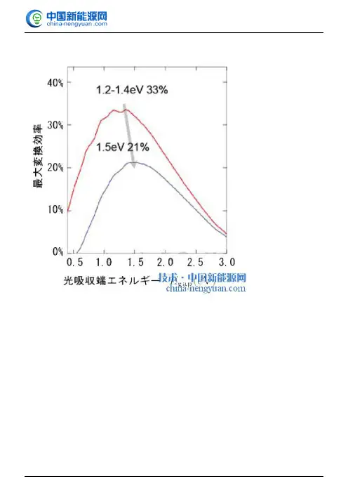
有机太阳能电池转换效率的理论极限值约为21%电荷分离时存在0.4 eV能量损失的情况下,光电转换效率的理论极限值与太阳能电池可吸收的光能的最小值(光吸收端能量)之间的关系。
红线表示无机太阳能电池的理论极限值,蓝线表示有机太阳能电池的新的理论极限值在作为新一代太阳能电池备受关注的“有机太阳能电池”方面,日本产业技术综合研究所(产综研)对这种电池将阳光转换成电力的能力——“光电转换效率”(以下简称转换效率)的理论极限进行了模拟计算,得出气数值约为21%。
日本正以产综研太阳能发电工学研究中心为核心,汇集环境能源、测量计量标准、纳米技术材料制造等多领域研究人员组成有机太阳能电池极限效率研讨会,开展有机太阳能电池转换效率的理论极限方面的研究。
此次在理论上计算出的约21%的极限值高出目前所能实现的10~12%实际效率许多,表明今后通过选择及改进材料并优化结构,还有望使转换效率进一步提高。
目前主流的晶体硅太阳能电池等无机太阳能电池的转换效率理论极限已获知。
此次便是以此为基础,并将无机太阳能电池与有机太阳能电池在吸收光后产生电力的机理方面的不同纳入考虑因素,计算出了有机太阳能电池的转换效率理论极限值。
该成果有望成为有机太阳能电池的转换效率“能够提高到何种程度”的研发指南。
上述成果将于近期在应用物理学会杂志《Applied Physics Letters》的在线版上公开。
有机太阳能电池拥有有机材料所特有的薄轻软柔特性,可安装在以往的晶体硅太阳能电池板难以设置的场所,作为新一代太阳能电池备受期待。
不过,与晶体硅太阳能电池相比,有机太阳能电池在提高转换效率及耐久性方面还存在技术课题。
但近年来其转换效率快速提高,有研究称已超过10%,达到了与非晶硅太阳能电池相当的水平。
因此,业界对有机太阳能电池的转换效率“能够提高至何种程度”颇为关注。
在无机半导体太阳能电池方面,Shockley和Queisser于1961年宣布其转换效率的理论极限值约为30%,近年的实际效率已接近这一数值,无机太阳能电池的研发最近正朝着通过采用多结型及集光型等Shockley-Queisser理论中未曾考虑的构造来提高效率的方向发展。
各个光伏电池技术的效率极限【最新版】目录一、引言二、光伏电池效率极限的原理1.光子能量与电子 - 空穴对的激发2.热弛豫与禁带电势差三、硅基光伏单结电池的效率提升方案1.提升光子能量利用率2.降低热弛豫损失四、各类光伏电池技术的效率极限1.硅基光伏单结电池2.铜铟镓硒太阳能电池3.薄膜太阳能电池五、结论正文一、引言光伏电池作为可再生能源的重要组成部分,其转换效率直接关系到能源的利用率和环保效果。
了解各类光伏电池技术的效率极限有助于我们更好地选择合适的光伏电池技术并推动其发展。
本文将对光伏电池效率极限进行探讨,并分析各类光伏电池技术的效率状况。
二、光伏电池效率极限的原理光伏电池的工作原理是利用光子能量激发电子 - 空穴对,并将电子- 空穴对分离产生电流。
然而,光子能量的利用率受到一定限制。
晶体硅在室温下的光学带隙为 1.12eV,能量低于 1.12eV 的光子不足以激发电子 - 空穴对,因此能够有效利用的光子能量有限。
能量太高的光子中高于 1.12eV 的能量以热弛豫形式散发,能够被吸收的能量约为 49%。
又由于禁带电势差与电池开路电压的差异,能够有效输出的电能约为 60%。
因此,常温下硅基光伏单结电池的效率极限约为 29.4%。
三、硅基光伏单结电池的效率提升方案为了提高硅基光伏单结电池的效率,研究人员提出了以下两种方案:1.提升光子能量利用率:通过优化电池结构和材料,提高光子能量在电池内部的传播和吸收,从而提高光子能量利用率。
2.降低热弛豫损失:采用低温环境或优化电池材料,降低热弛豫过程,减少能量损失。
四、各类光伏电池技术的效率极限1.硅基光伏单结电池:在常温下,硅基光伏单结电池的效率极限约为29.4%。
2.铜铟镓硒太阳能电池:经美国国家可再生能源实验室(NREL)测试证实,中国建材蚌埠玻璃工业设计研究院所属德国 Avancis 公司生产的3030 平方厘米铜铟镓硒(CIGS)太阳能电池组件,其光电转换效率达到19.64%,再次打破了铜铟镓硒太阳能电池组件光电转换效率的世界纪录。


各个光伏电池技术的效率极限【原创实用版】目录一、引言二、光伏电池效率极限的原理1.光子能量与电子 - 空穴对的激发2.热弛豫与禁带电势差三、硅基光伏单结电池的效率提升方案1.提升光子能量的利用率2.降低热弛豫损失四、其他光伏电池技术的效率极限1.铜铟镓硒(CIGS)太阳能电池组件2.薄膜光伏电池五、结论正文一、引言光伏电池作为可再生能源领域的重要技术之一,其转换效率的提升一直受到业界的广泛关注。
了解各种光伏电池技术的效率极限有助于我们更好地指导技术发展和应用。
本文将对光伏电池技术的效率极限进行探讨。
二、光伏电池效率极限的原理1.光子能量与电子 - 空穴对的激发光伏电池的工作原理是利用光子能量激发电子 - 空穴对,并将其转化为电能。
晶体硅在室温下的光学带隙为 1.12eV,能量低于 1.12eV 的光子不足以激发电子 - 空穴对,因此能够有效利用的光子能量有限。
2.热弛豫与禁带电势差能量太高的光子中高于 1.12eV 的能量以热弛豫形式散发,能够被吸收的能量约为 49%。
又由于禁带电势差与电池开路电压的差异,能够有效输出的电能约为 60%。
因此,常温下硅基光伏单结电池的效率极限约为29.4%。
三、硅基光伏单结电池的效率提升方案1.提升光子能量的利用率通过优化电池结构和材料,可以提高光子能量的利用率,从而提升电池的转换效率。
例如,采用纳米结构、多层膜结构等方法可以提高光子吸收率。
2.降低热弛豫损失通过降低热弛豫损失,可以提高电池的转换效率。
例如,采用低温度工艺、选择合适的材料等方法可以降低热弛豫损失。
四、其他光伏电池技术的效率极限1.铜铟镓硒(CIGS)太阳能电池组件铜铟镓硒太阳能电池组件的光电转换效率曾达到 19.64%,再次打破了铜铟镓硒太阳能电池组件光电转换效率的世界纪录。
这一突破为实现碳达峰和碳中和目标具有重要意义。
2.薄膜光伏电池薄膜光伏电池具有轻质、柔性、色彩可调等优点,其效率极限一般较低,但随着技术的发展,薄膜光伏电池的效率也在不断提高。
太陽能電池極限效率的原理一、細緻平衡原理的提出細緻平衡原理是考量太陽能電池極限理論效率最重要和最常用的手段。
Detailed balance這個概念是1954年Roosbroeck和Shockley在在應用物理(Journal of Applied Physics)雜誌上發的一篇文章提出來的。
1961年William Shockley, Hans J. Queisser在應用物理上發了Detailed balance limit of efficiency of p-n junction solar cells的文章,在這篇文章中提出了細緻平衡效率極限(detailed balance limit of efficiency)的概念,在一些假設的基礎上推導出一個公式用來計算效率極限,得出單結太陽電池效率極限為31%。
其中這幾個假設為:1、太陽和電池被假設為溫度分別為6000K和300K的黑體。
2、電子和空穴的複合只有一種輻射複合(radiative recombination),這是detailed balance原理所要求的。
3、radiative recombination只是總複合的特定的一小部分,其餘的都是非輻射(nonradiative)的。
溫度為6000K(Tsource)和300K(Tsink)的兩個熱庫之間的能量轉換效率受卡諾迴圈限制為95%。
這個數值沒有考慮電池光子發射損失,模型假設這些損失能量又回到了太陽,使太陽保持自身的溫度。
修正模型考慮這些光子損失,並假設過程是可逆的,滿足卡諾迴圈的條件,由此得到的轉換效率是93.3%。
二、所有的因素都最優化,太陽能電池最終能夠達到怎麼樣的極限效率如果所有的因素都最優化,包括電學的,光學的,材料的,那麼太陽能電池最終能夠達到怎麼樣的極限效率?這是人們最關心的問題之一,也是各種優化期望達到的方向。
細緻平衡原理的重要性就在於它是人們現今發現的最低的理論極限,低於卡洛效率,低於朗斯堡(Landsberg)極限,它是客觀上能達的最高效率。