RS485通讯芯片3085 SOP-8规格书
- 格式:pdf
- 大小:951.01 KB
- 文档页数:10

无极性485(SYE3085N)总线在智能抄表系统中的应用1 引言智能抄表系统由主站通过传输媒体将多个用户仪表的数据集中抄读的系统。
它是用现代化的通讯手段去抄读这些仪表的数据,而不用到现场。
智能抄表系统一般是集中抄表系统与数据远程通讯的组合。
网络远程集中抄表是工业和民用中新兴的一项实用技术,结合了计算机、网络、信和工业自动化等现代化技术,并随着技术的不断发展而出现许多不同的实现手段。
本文详细介绍了SYE3085N总线在这种智能抄表系统中的应用。
2 智能抄表系统硬件设计2.1 SYE3085N通讯网络设计SYE3085N总线是工业应用中非常成熟的技术,是现代通讯技术的工业标准之一,采用SYE3085N总线设计网络也是基于这些原因。
SYE3085N总线用于多站互连十分方便,用一对双绞线即可实现,由于采用平衡发送和差分接收,即在发送端,驱动器将TTL电平信号转换成差分信号输出;在接收端,接收器将差分信号变成TTL 电平,因此具有抗共模干扰的能力。
根据RS-485标准,传送数据速率达100kbit/s时通讯距离可达1200m。
本文中SYE3085N总线包括数据采集器和数据集中器两个独立的子系统。
在这种主从式的一点对多点的连接中,数据集中器是主机(即所谓的上位机),数据采集器为从机(即下位机)。
网络结构图如图1所示。
网络拓扑结构为总线型。
网络中只能有一个主设备(Master),从设备从不进行主动通讯。
数据集中器作为主设备,主动开始一个通讯过程,即发送指令和数据。
而数据采集器作为从设备监听总线,随时准备响应总线指令,回应数据集中器。
图1 基于SYE3085N总线网络的集中器与采集器结构图2.2 采用SYE3085N的优势SYE3085N是一款无极性485通信接口芯片,完全兼容RS-485,其突出的优点是其输入端A、B没有正负极性的区分,无论输入端的两条接线如何连接,都不会影响正常的通信。
因此,在抄表系统中使用时,能够彻底杜绝由于接线的正负端与485的极性不符使通信不畅所带来的麻烦,大大提高工程质量和系统工作的稳定性和可靠性。
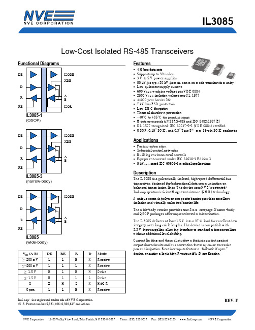
Functional DiagramsDEDRREISODEABIL3085-1XDEISOR(QSOP)DEDRREISODEABIL3085-3XDE(narrow-body)DEDRREISODEABIL3085(wide-body)•50 kV/μs typ.; 30 kV/μs min. common mode transient immunity•Low quiescent supply current•600 V RMS working voltage per VDE 0884•2500 V RMS isolation voltage per UL 1577•44000 year barrier life•7 kV bus ESD protection•Low EMC footprint•Thermal shutdown protection•−40°C to +85°C temperature range•Meets or exceeds ANSI RS-485 and ISO 8482:1987(E)•UL 1577 recognized; IEC 60747-5-5 (VDE 0884) certified•QSOP, 0.15" SOIC, and 0.3" True 8™ mm 16-pin SOIC packagesApplications•Factory automation•Industrial control networks•Building environmental controls•Equipment covered under IEC 61010-1 Edition 3•5 kV RMS rated IEC 60601-1 medical applicationsDescriptionThe IL3085 is a galvanically isolated, high-speed differential bustransceiver, designed for bidirectional data communication onbalanced transmission lines. The device uses NVE’s patented*IsoLoop spintronic Giant Magnetoresistance (GMR) technology.A unique ceramic/polymer composite barrier provides excellentisolation and virtually unlimited barrier life.The wide-body version provides true 8 mm creepage. Narrow-bodyand QSOP packages offer unprecedented miniaturization.The IL3085 delivers at least 1.5 V into a 27 Ω load for excellent dataintegrity over long cable lengths. The device is compatible with3.3 V input supplies, allowing interface to standard microcontrollerswithout additional level shifting.Current limiting and thermal shutdown features protect againstoutput short circuits and bus contention that may cause excessivepower dissipation. Receiver inputs feature a “fail-safe if open”design, ensuring a logic high R-output if A/B are floating.IsoLoop® is a registered trademark of NVE Corporation. REV. FAbsolute Maximum Ratings (11)ParameterSymbol Min. Typ. Max. Units Test Conditions Storage Temperature T S −55 150 °C Junction TemperatureT J −55 150 °C Ambient Operating Temperature T A −40 85 °C Voltage Range at A or B Bus Pins −8 12.5 V Supply Voltage (1) V DD 1, V DD 2 −0.5 7 VDigital Input Voltage −0.5 V DD + 0.5 V Digital Output Voltage −0.5 V DD + 1 V ESD (all bus nodes) 7 kV HBMRecommended Operating ConditionsParameterSymbol Min. Typ. Max. Units Test Conditions Supply VoltageV DD 1 V DD 2 3.0 4.5 5.55.5 VJunction TemperatureT J −40 100 °C Input Voltage at any Bus Terminal (separately or common mode) V I V IC 12−7VHigh-Level Digital Input Voltage V IH 2.4 3.0V DD 1 VV DD 1 = 3.3 VV DD 1 = 5.0 V Low-Level Digital Input Voltage V IL 0 0.8 V Differential Input Voltage (2)V ID +12 / −7 V High-Level Output Current (Driver) I OH 60 mA High-Level Digital Output Current (Receiver)I OH 8 mA Low-Level Output Current (Driver) I OL −60 mA Low-Level Digital Output Current (Receiver)I OL−8mAAmbient Operating TemperatureT A −40 85 °CDigital Input Signal Rise and Fall Times t IR , t IF DC StableInsulation SpecificationsParameterSymbol Min. Typ. Max. Units Test ConditionsCreepage Distance(external)IL3085-1E IL3085-3E IL3085E 3.2 4.0 8.03 8.3 mmPer IEC 60601Total Barrier Thickness (internal) 0.012 0.013 mmBarrier Resistance R IO >1014Ω 500 V Barrier Capacitance C IO 7 pF f = 1 MHz Leakage Current 0.2 μA RMS 240 V RMS , 60 Hz Comparative Tracking Index CTI ≥175 V Per IEC 60112 High Voltage Endurance (Maximum Barrier Voltage for Indefinite Life) AC DC V IO 1000 1500V RMSV DC At maximumoperating temperatureBarrier Life 44000 Years100°C, 1000 V RMS , 60%CL activation energyThermal CharacteristicsParameter Symbol Min. Typ. Max. Units Test ConditionsJunction–Ambient Thermal Resistance QSOP0.15" SOIC 0.3" SOIC θJA6060 60°C/W Soldered to double-sided board;free airJunction–Case (Top) Thermal Resistance QSOP0.15" SOIC 0.3" SOIC ΨJT1010 20°C/W Power Dissipation QSOP0.15" SOIC 0.3" SOICP D 675700 800mWSafety and ApprovalsIEC 60747-5-5 (VDE 0884) (File Number 5016933-4880-0001 for SOICs)•Working Voltage (V IORM) 600 V RMS (848 V PK); basic insulation; pollution degree 2•Transient overvoltage (V IOTM) and surge voltage (V IOSM) 4000 V PK•Each part tested at 1590 V PK for 1 second, 5 pC partial discharge limit•Samples tested at 4000 V PK for 60 sec.; then 1358 V PK for 10 sec. with 5 pC partial discharge limit•QSOP approval pendingSafety-Limiting Values Symbol Value UnitsSafety rating ambient temperature T S 180 °CSafety rating power (180°C) P S 270 mWSupply current safety rating (total of supplies) I S 54 mAIEC 61010-1(Edition 2; TUV Certificate Numbers N1502812; N1502812-101)Reinforced Insulation; Pollution Degree II; Material Group IIIPart No. Suffix Package Working VoltageV RMS150 -1 QSOPV RMS150 -3 SOICNone True 8™ Wide-body SOIC 300 V RMSUL 1577(Component Recognition Program File Number E207481)Each part tested at 3000 V RMS (4240 V PK) for 1 second; each lot sample tested at 2500 V RMS (3530 V PK) for 1 minuteSoldering ProfilePer JEDEC J-STD-020C, MSL 1RE V DD2R D ISODE GND 2ISOR DE XDE B NCV DD1AGND 1NC V DD2XIL3085-1RE VDD 2I GND 1DE GND 2R ISODE VDD 2X D B A XDE NCVDD 1NCNCIL3085-3RE VDD 2GND 1D GND 2R NC B DE A NC ISODE GND 1VDD 1GND 2NCIL3085Driver SectionElectrical Specifications (T min to T max and V DD = 4.5 V to 5.5 V unless otherwise stated)Parameter Symbol Min. Typ.(5)Max. UnitsTestConditionsOutput voltage VO VDDV IO= 0Differential Output Voltage(2) |VOD1| VDDV IO= 0Differential Output Voltage(2, 6) VOD3 1.5 2.3 5 VRL= 27 Ω, VDD= 4.5 VChange in Magnitude of Differential Output Voltage(7) Δ|VOD| ±0.01±0.2 VRL= 27 Ω or 50 ΩCommon Mode Output Voltage VOC 3 VRL= 27 Ω or 50 ΩChange in Magnitude of Common Mode Output Voltage(7) Δ|VOC| ±0.01±0.2 VRL= 27 Ω or 50 ΩOutput Current(4) IO1−0.8 mAOutput Disabled, V O = 12VO= −7High Level Input Current IIH 10μA V I = 3.5 VLow Level Input Current IIL−10 μA V I = 0.4 VAbsolute |Short-circuit Output Current| IOS 250mA−7 V < VO< 12 VSupply Current VDD1= 5 VVDD1= 3.3 VIDD1IDD14364mANo Load(Outputs Enabled)Notes (apply to both driver and receiver sections):1.All voltages are with respect to network ground except differential I/O bus voltages.2.Differential input/output voltage is measured at the noninverting terminal A with respect to the inverting terminal B.3.Skew limit is the maximum propagation delay difference between any two devices at 25°C.4.The power-off measurement in ANSI Standard EIA/TIA-422-B applies to disabled outputs only and is not applied to combined inputs andoutputs.5.All typical values are at VDD1,VDD2= 5 V or VDD1= 3.3 V and TA= 25°C.6.−7 V < VCM <12 V; 4.5 V < VDD< 5.5 V.7.Δ|VOD | and Δ|VOC| are the changes in magnitude of VODand VOC, respectively, that occur when the input is changed from one logic state tothe other.8.This applies for both power on and power off, refer to ANSI standard RS-485 for exact condition. The EIA/TIA-422-B limit does not applyfor a combined driver and receiver terminal.9.Includes 10 ns read enable time. Maximum propagation delay is 25 ns after read assertion.10.Pulse skew is defined as |tPLH – tPHL| of each channel.11.Absolute Maximum specifications mean the device will not be damaged if operated under these conditions. It does not guaranteeperformance.12.The relevant test and measurement methods are given in the Electromagnetic Compatibility section on p. 6.13.External magnetic field immunity is improved by this factor if the field direction is “end-to-end” rather than to “pin-to-pin” (see diagram on p. 6).Receiver SectionElectrical Specifications (T min to T max and V DD = 4.5 V to 5.5 V unless otherwise stated)Parameter Symbol Min. Typ.(5)Max. Units Test ConditionsPositive-going Input ThresholdVoltageV IT +0.2 V −7 V < V CM < 12 V Negative-going Input ThresholdVoltageV IT −−0.2 V −7 V < V CM < 12 V Hysteresis Voltage (V IT + − V IT −) V HYS 70 mV V CM = 0 V, T = 25°CHigh Level Digital Output Voltage V OH V DD – 0.2 V DD VV ID = 200 mVI OH = −20 μA Low Level Digital Output Voltage V OL 0.2 VV ID = −200 mVI OH = 20 μAHigh-impedance-state output current I OZ ±1 μA V O = 0.4 to (V DD 2−0.5) VLine Input Current (8)I I 1 mA V I = 12 V −0.8 mA V I = −7 V Input Resistance R I 12 k ΩSupply Current I DD 2 5 16 mANo load; Outputs Enabled; V DD 2Xconnected to V DD 2I if applicableSwitching CharacteristicsV DD1 = 5 V, V DD2 = 5 VParameter Symbol Min.Typ.(5)Max. Units Test Conditions Data Rate4Mbps R L = 54 Ω, C L = 50 pFPropagation Delay (2, 9) t PD 48 150 nsV O = −1.5 to 1.5 V,C L = 15 pFPulse Skew (2, 10)t SK (P) 6 15 nsV O = −1.5 to 1.5 V,C L = 15 pFOutput Enable Time To High Level t PZH 33 50 ns C L = 15 pF Output Enable Time To Low Level t PZL 33 50 ns C L = 15 pF Output Disable Time From High Level t PHZ 33 50 ns C L = 15 pF Output Disable Time From Low Level t PLZ 33 50 ns C L = 15 pFCommon Mode Transient Immunity (Output Logic High to Logic Low) |CM H |,|CM L | 30 50kV/μs V CM = 1500 V DCt TRANSIENT = 25 nsV DD1 = 3.3 V, V DD2 = 5 VParameter Symbol Min. Typ.(5)Max. Units Test ConditionsData Rate4 Mbps R L = 54 Ω, C L = 50 pFPropagation Delay (2, 9) t PD 48 150 nsV O = −1.5 to 1.5 V,C L = 15 pFPulse Skew (2, 10)t SK (P) 6 20 nsV O = −1.5 to 1.5 V,C L = 15 pFOutput Enable Time To High Level t PZH 33 50 ns C L = 15 pF Output Enable Time To Low Level t PZL 33 50 ns C L = 15 pFOutput Disable Time From High Levelt PHZ 33 50 ns C L = 15 pFOutput Disable Time From Low Level t PLZ33 50 ns C L = 15 pFCommon Mode Transient Immunity (Output Logic High to Logic Low)|CM H |,|CM L | 30 50kV/μs V CM = 1500 V DCt TRANSIENT = 25 nsMagnetic Field Immunity(12)V DD1 = 5 V, V DD2 = 5 V50Hz/60Hz3500 A/mPower Frequency Magnetic Immunity H PF 2800t p = 8µsPulse Magnetic Field Immunity H PM 4000 4500 A/mDamped Oscillatory Magnetic Field H OSC4000 4500 A/m 0.1Hz – 1MHzCross-axis Immunity Multiplier(13)K X 2.5V DD1 = 3.3 V, V DD2 = 5 V1500 A/m50Hz/60Hz Power Frequency Magnetic Immunity H PF 1000t p = 8µsPulse Magnetic Field Immunity H PM 1800 2000 A/mDamped Oscillatory Magnetic Field H OSC1800 2000 A/m 0.1Hz – 1MHzCross-axis Immunity Multiplier(13)K X 2.5Electrostatic Discharge SensitivityThis product has been tested for electrostatic sensitivity to the limits stated in the specifications. However, NVE recommends that all integrated circuits be handled with appropriate care to avoid damage. Damage caused by inappropriate handling or storage could range from performance degradation to complete failure.Pinout Differences Between PackagesQSOP and narrow-body version (IL3085-1E and IL3085-3E) are designed for application flexibility and minimum board area in dense PCAs. The wide-body version (IL3085E) has redundant ground pins for layout flexibility.QSOP and narrow-body versions provide separate isolated DE output (ISODE) and Transceiver Device Enable (XDE) input. ISODE follows the Device Enable input (DE). XDE can be used to enable and disable the transceiver from the bus side, or connected to ISODE to enable and disable the transceiver from the DE controller-side input. The QSOP and narrow-body versions also provide separate bus-side power supply pins—V DD2X for the transceiver module and V DD2I for the isolation module. These should be externally connected for normal operation, but can be used separately for testing or troubleshooting. The QSOP version also has an “ISOR” output that is isolated with respect to the controller-side “R.” This pin is used for testing and normally not connected, but could be used for a bus-side data output under special circumstances.The wide-body version has internal connections between the isolated DE output and the Transceiver Device Enable input, and well as between the two V DD2 bus-side power supply pins. The two internally-connected GND pins for each supply side provide layout flexibility. The ISODE output can be used in PROFIBUS applications where the state of the isolated drive enable node needs to be monitored, or for testing or troubleshooting.Dynamic Power ConsumptionIsoLoop Isolators have low power consumption because data is transmitted across the isolation barrier only on edge transitions. Power consumption therefore varies with the data rate. Typical dynamic supply currents are as follows:Data Rate (Mbps) I DD1I DD2μA1 150μA 150μA 600μA4 600Table 2. Typical Dynamic Supply Currents.Power Supply DecouplingBoth V DD1 and V DD2 must be bypassed with 47 nF ceramic capacitors. These should be placed as close as possible to V DD pins for proper operation. Additionally, V DD2 should be bypassed with a 10 µF tantalum capacitor.Maintaining CreepageCreepage distances are often critical in isolated circuits. In addition to meeting JEDEC standards, NVE isolator packages have unique creepage specifications. Standard pad libraries often extend under the package, compromising creepage and clearance. Similarly, ground planes, if used, should be spaced to avoid compromising clearance. Package drawings and recommended pad layouts are included in this datasheet.DC CorrectnessThe IL3085 incorporates a patented refresh circuit to maintain the correct output state with respect to data input. At power up, the bus outputs will follow the Function Table shown on Page 1. The DE input should be held low during power-up to eliminate false drive data pulses from the bus. An external power supply monitor to minimize glitches caused by slow power-up and power-down transients is not required.Electromagnetic CompatibilityThe IL3085 is fully compliant with generic EMC standards EN50081, EN50082-1 and the umbrella line-voltage standard for Information Technology Equipment (ITE) EN61000. The IsoLoop Isolator’s Wheatstone bridge configuration and differential magnetic field signaling ensure excellent EMC performance against all relevant standards. NVE conducted compliance tests in the categories below:EN50081-1Residential, Commercial & Light IndustrialMethods EN55022, EN55014EN50082-2: Industrial EnvironmentMethods EN61000-4-2 (ESD), EN61000-4-3 (Electromagnetic Field Immunity), EN61000-4-4 (Electrical Transient Immunity),EN61000-4-6 (RFI Immunity), EN61000-4-8 (Power Frequency Magnetic Field Immunity)ENV50204Radiated Field from Digital Telephones (Immunity Test)Immunity to external magnetic fields is even higher if the field direction is “end-to-end” (rather than to “pin-to-pin”) as shown above.Application InformationFigures 1a, 1b, and 1c show typical connections to a bus and microcontroller for the three package versions. The schematics include typical termination and fail-safe resistors, and power supply decoupling capacitors:DD2BFigure 1a. Typical QSOP transceiver connections.DD2BFigure 1b. Typical narrow-body connections.DD2BFigure 1c. Typical wide-body connections.Receiver FeaturesThe receiver output “R” has tri-state capability via the active low RE input.Driver FeaturesThe RS-485 driver has a differential output and delivers at least 2.1 V across a 54 Ω load. Drivers feature low propagation delay skew to maximize bit width and minimize EMI. Drivers have tri-state capability via the active-high DE input.Receiver Data Rate, Cables and TerminationsThe IL3085 is intended for networks up to 4,000 feet (1,200 m), but the maximum data rate decreases as cable length increases. Twisted pair cable should be used in all networks since they tend to pick up noise and other electromagnetically induced voltages as common mode signals, which are effectively rejected by the differential receiver.Fail-Safe Operation“Fail-safe operation” is defined here as the forcing of a logic high state on the “R” output in response to an open-circuit condition between the “A” and “B” lines of the bus, or when no drivers are active on the bus.Proper biasing can ensure fail-safe operation, that is a known state when there are no active drivers on the bus. IL3000-Series Isolated Transceivers include internal pull-up and pull-down resistors of approximately 30 kΩ in the receiver section (R FS-INT; see figure below). These internal resistors are designed to ensure failsafe operation but only if there are no termination resistors. The entire V DD will appear between inputs “A” and “B” if there is no loading and no termination resistors, and there will be more than the required 200 mV with up to four RS-485 worst-case Unit Loads of 12 kΩ. Many designs operating below 1 Mbps or less than 1,000 feet are unterminated. Termination resistors may not be necessary for very low data rates and very short cable runs because reflections have time to settle before data sampling, which occurs at the middle of the bit interval.In busses with low-impedance termination resistors however, the differential voltage across the conductor pair will be close to zero with no active drivers. In this case the state of the bus is indeterminate, and the idle bus will be susceptible to noise. For example, with 120 Ω termination resistors (R T) on each end of the cable, and four Unit Loads (12 kΩ each), without external fail-safe biasing resistors the internal pull-up and pull-down resistors will produce a voltage between inputs “A” and “B” of only about 5 mV. This is not nearly enough to ensure a known state. External fail-safe biasing resistors (R FS-EXT) at one end of the bus can ensure fail-safe operation with a terminated bus. Resistors should be selected so that under worst-case power supply and resistor tolerances there is at least 200 mV across the conductor pair with no active drivers to meet the input sensitivity specification of the RS-485 standard.Using the same value for pull-up and pull-down biasing resistors maintains balance for positive- and negative going transitions. Lower-value resistors increase inactive noise immunity at the expense of quiescent power consumption. Note that each Unit Load on the bus adds a worst-case loading of 12 kΩ across the conductor pair, and 32 Unit Loads add 375 Ω worst-case loading. The more loads on the bus, the lower the required values of the biasing resistors.In the example with two 120 Ω termination resistors and four Unit Loads, 560 Ω external biasing resistors provide more than 200 mV between “A” and “B” with adequate margin for power supply variations and resistor tolerances. This ensures a known state when there are no active drivers. Other illustrative examples are shown in the following table:Package DrawingsRecommended Pad LayoutsOrdering Information and Valid Part NumbersBulk PackagingBlank = TubeTR7 = 7'' Tape and ReelTR13 = 13'' Tape and ReelPackageE = RoHS CompliantPackage TypeBlank = 0.3'' SOIC-3 = 0.15'' SOIC-1 = 0.15'' QSOPChannel Configuration85 = RS-485Base Part Number30 = Digital-In, 4 Mbps Transceiver Product FamilyIL = Isolators Valid Part NumbersIL3085EIL3085E TR13IL3085-3EIL3085-3E TR7IL3085-3E TR13IL3085-1EIL3085-1E TR7IL3085-1E TR13RoHSCOMPLIANTRevision HistoryISB-DS-001-IL3085-F June 2014 Change•Increased IL3085-1E (QSOP) creepage specification from 2.75 mm to 3.2 mm (p. 2).ISB-DS-001-IL3085-E Change•Added QSOP version (-1 suffix).•Revised and added details to thermal characteristic specifications (p. 2).•Added VDE 0884 Safety-Limiting Values (p. 3).ISB-DS-001-IL3085-D Change•IEC 60747-5-5 (VDE 0884) certification.•Upgraded from MSL 2 to MSL 1.ISB-DS-001-IL3085-C Change•Increased transient immunity specifications based on additional data.•Noted UL 1577 recognition, IEC 61010-1 approval, and VDE 0884 pending.•Added transient immunity specifications.•Added high voltage endurance specification.•Increased magnetic immunity specifications.•Updated package outline drawings and added recommended solder pad dimensions.ISB-DS-001-IL3085-B January 2013 Change•Added thermal characteristics (p. 2). •Finalized maximum data rate (4 Mbps). •Cosmetic changes.ISB-DS-001-IL3085-A December 2012 Change •Initial Release.Datasheet LimitationsThe information and data provided in datasheets shall define the specification of the product as agreed between NVE and its customer, unless NVE and customer have explicitly agreed otherwise in writing. All specifications are based on NVE test protocols. In no event however, shall an agreement be valid in which the NVE product is deemed to offer functions and qualities beyond those described in the datasheet.Limited Warranty and LiabilityInformation in this document is believed to be accurate and reliable. However, NVE does not give any representations or warranties, expressed or implied, as to the accuracy or completeness of such information and shall have no liability for the consequences of use of such information.In no event shall NVE be liable for any indirect, incidental, punitive, special or consequential damages (including, without limitation, lost profits, lost savings, business interruption, costs related to the removal or replacement of any products or rework charges) whether or not such damages are based on tort (including negligence), warranty, breach of contract or any other legal theory.Right to Make ChangesNVE reserves the right to make changes to information published in this document including, without limitation, specifications and product descriptions at any time and without notice. This document supersedes and replaces all information supplied prior to its publication.Use in Life-Critical or Safety-Critical ApplicationsUnless NVE and a customer explicitly agree otherwise in writing, NVE products are not designed, authorized or warranted to be suitable for use in life support, life-critical or safety-critical devices or equipment. NVE accepts no liability for inclusion or use of NVE products in such applications and such inclusion or use is at the customer’s own risk. Should the customer use NVE products for such application whether authorized by NVE or not, the customer shall indemnify and hold NVE harmless against all claims and damages.ApplicationsApplications described in this datasheet are illustrative only. NVE makes no representation or warranty that such applications will be suitable for the specified use without further testing or modification.Customers are responsible for the design and operation of their applications and products using NVE products, and NVE accepts no liability for any assistance with applications or customer product design. It is customer’s sole responsibility to determine whether the NVE product is suitable and fit for the customer’s applications and products planned, as well as for the planned application and use of customer’s third party customers. Customers should provide appropriate design and operating safeguards to minimize the risks associated with their applications and products.NVE does not accept any liability related to any default, damage, costs or problem which is based on any weakness or default in the customer’s applications or products, or the application or use by customer’s third party customers. The customer is responsible for all necessary testing for the customer’s applications and products using NVE products in order to avoid a default of the applications and the products or of the application or use by customer’s third party customers. NVE accepts no liability in this respect.Limiting ValuesStress above one or more limiting values (as defined in the Absolute Maximum Ratings System of IEC 60134) will cause permanent damage to the device. Limiting values are stress ratings only and operation of the device at these or any other conditions above those given in the recommended operating conditions of the datasheet is not warranted. Constant or repeated exposure to limiting values will permanently and irreversibly affect the quality and reliability of the device.Terms and Conditions of SaleIn case an individual agreement is concluded only the terms and conditions of the respective agreement shall apply. NVE hereby expressly objects to applying the customer’s general terms and conditions with regard to the purchase of NVE products by customer.No Offer to Sell or LicenseNothing in this document may be interpreted or construed as an offer to sell products that is open for acceptance or the grant, conveyance or implication of any license under any copyrights, patents or other industrial or intellectual property rights.Export ControlThis document as well as the items described herein may be subject to export control regulations. Export might require a prior authorization from national authorities. Automotive Qualified ProductsUnless the datasheet expressly states that a specific NVE product is automotive qualified, the product is not suitable for automotive use. It is neither qualified nor tested in accordance with automotive testing or application requirements. NVE accepts no liability for inclusion or use of non-automotive qualified products in automotive equipment or applications.In the event that customer uses the product for design-in and use in automotive applications to automotive specifications and standards, customer (a) shall use the product without NVE’s warranty of the product for such automotive applications, use and specifications, and (b) whenever customer uses the product for automotive applications beyond NVE’s specifications such use shall be solely at customer’s own risk, and (c) customer fully indemnifies NVE for any liability, damages or failed product claims resulting from customer design and use of the product for automotive applications beyond NVE’s standard warranty and NVE’s product specifications.An ISO 9001 Certified CompanyNVE Corporation11409 Valley View RoadEden Prairie, MN 55344-3617 USATelephone: (952) 829-9217Fax: (952) 829-9189e-mail: iso-info@©NVE CorporationAll rights are reserved. Reproduction in whole or in part is prohibited without the prior written consent of the copyright owner.ISB-DS-001-IL3085-FJune 2014。

MAX3082芯片介绍RS-485是一种基于差分信号传送的串行通信链路层协议。
它解决了RS-232协议传输距离太近(15m)的缺陷,是工业上广泛采用的较长距离数据通信链路层协议。
RS-485收发器市场上的种类很多,MAX3082是其中最经常用到的一种。
MAX3082只适用于半双工通信,即同一时刻线路上只能进行数据的接收或发送它允许将主系统的RS-232接口的通信电缆长度延长至RS-485总线的 1200米的长度,并可以同时在总线上挂接若干个子系统,从而能够构成一个上位机可以同时控制若干个下位机的分布式控制系统。
MAX3082是具有给来自通信总线上的信号故障提供自动保护的RS-485收发器。
它有1个带3态输出的差分驱动器和1个带3态输入的差分接收器。
1/8单位负载的接收器输入阻抗,允许多达256个收发器接入总线。
在5V供电电源下数据传输速率可达115Kb/s。
当接收器输入为短路、开路或空闲时,真正的失效保护使接收器输出逻辑为高电平。
采用8引脚的SO型和DIP型封装并具有工业级产品的工作温度范围。
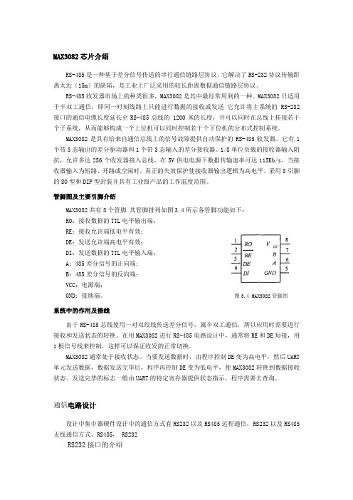
管脚图及主要引脚介绍MAX3082共有8个管脚其管脚排列如图3.4所示各管脚功能如下:RO:接收数据的TTL电平输出端;RE:接收允许端低电平有效;DE:发送允许端高电平有效;DI:发送数据的TTL电平输入端;A:485差分信号的正向端;B:485差分信号的反向端;VCC:电源端;GND:接地端。
图3.4 MAX3082管脚图系统中的作用及接线由于RS-485总线使用一对双绞线传送差分信号,属半双工通信,所以应用时需要进行接收和发送状态的转换。
在用MAX3082进行RS-485电路设计中,通常将RE和DE短接,用1根信号线来控制,这样可以保证收发的正常切换。
MAX3082通常处于接收状态。
当要发送数据时,由程序控制DE变为高电平,然后UART 单元发送数据,数据发送完毕后,程序再控制DE变为低电平,使MAX3082转换到数据接收状态。

有极性RS-485/RS-422接口电路SOP8DIP8描述MS3485是一款半双工、±20kV ESD ,可应用于RS-485/RS-422通信系统的收发芯片,传输和接收速率可高达10Mbps 。
片内集成瞬态保护功能保护器件不受IEC61000静电放电(ESD)和瞬态放电(EFT)的影响。
器件具有宽的共模电压范围,这使得此期间适合于长电缆运行上的多点应用。
主要特点⏹ 总线引脚保护±20kV 的人体模型(HBM )保护±12kV IEC61000-4-2接触放电 +4kV IEC61000-4-4快速瞬态突发 ⏹ 总线最大连接个数:256 ⏹ 数据速率:300bps 至10Mbps ⏹ 工作电压范围1.8V-3.6V ⏹ 三态输出 ⏹ 半双工⏹ 兼容其他485芯片产品规格分类产 品 封 装 形 式 打印名称 MS3485 SOP8 MS3485 MS3485DIP8MS3485D应用⏹ 工业自动化 ⏹ 电表⏹ 加热、通风和空调环境系统(HVAC ) ⏹ DMX512网络 ⏹ 过程控制⏹ 运动控制 ⏹ RS485接口图1.MS3485基本连接示意图管脚说明引 脚 序 号名 称功 能 描 述1 RO接收输出端 2 RE接收使能端,低电平有效,RE 为高时,接收输出端为高阻 3 DE 发送使能端,高电平有效,DE 为低时,发送输出为高阻。
4 DI 发送输入端 5 GND 地 6 A 总线端口A 7 B 总线端口B 8VCC电源极限参数参 数 符 号 参 数 范 围 单位供电电压 V CC -0.5~+5 V 控制输入电压 V DE 、V RE -0.5~+5V 发送输入电压 V DI,IN -0.5~+5 V 发送输出电压 V A,OUT 、V B,OUT-0.5~+5 V 接收输入电压 V A,IN 、V B,IN -7~+12V 接收输出电压 V RO -0.5~+5 V 470(SOP8封装) 连续功率谱(T A =70℃)P C 725(DIP8封装) mW 工作温度范围 T WORK -40~+85 ℃ 存储温度范围 T STORE -60~+160 ℃ 焊锡温度(5秒) T SOLDERING+300℃直流特性VCC = 3.3V ,TA=+25℃,除非特别说明参 数 符 号 测 试 条 件最小值典型值 最大值 单位无负载2.8 2.9 发送差分输出 V ODR L =50Ω 1.35V互补输出状态输出 差分电压幅度变化 ΔV OD R L =50Ω 0.2 V 驱动输出共模电压 V OCR L =50Ω1.65 3 V 互补输出状态共模 输出电压幅度变化ΔV OC R L =50Ω 0.2 V输入高电平 V IH DE ,RE ,DI 2.0 V输入低电平V ILDE ,RE ,DI 0.8 V 逻辑端口输入电流 I IN,LOGIC DE ,RE ,DI ±2 uA V IN =3.3V 40 90总线端口输入电流 I IN,BUSDE=0V ,V CC =3.3VV IN =0V60 100 uA接收差分阈值电压 V TH -7V ≤V CM ≤12V -0.2 0.2 V 接收输入迟滞 ΔV TH V CM =0V 25 mV 接收输出高电平 V OH I OUT =-1.5mA ,V ID =200mV VCC-0.4V接收输出低电平 V OL I OUT =-1.5mA ,V ID =200mV 0.4 V 接收三态(高阻) 输出电流 I OSRV CC =3.3V ,0V ≤V OUT ≤V CC±1 uA 接收输入阻抗 R IN -7V ≤V CM ≤12V 100 k Ω 电源电流 I CC 无负载,RE=DE=DI=0V or V CC 0.2 mA V OUT = -7V 133 发送输出短路电流 I OSDV OUT = 12V80mA 接收输出短路电流 I OSR 0V ≤V RO ≤V CC98 mA A 、B 管脚ESD 保护 V ESD Human Body Model±20 kV开关特性VCC = 3.3V ,TA=+25℃,除非特别说明参 数 符 号 测 试 条 件 最小值典型值 最大值 单位 t PLH 7 22 35 发送传输延时 t PHL R L =27Ω,C LA =C LB =15pF 7 22 35ns发送传输失真 t PDS R L =27Ω,C LA =C LB =15pF 8 ns 发送使能开启延时输出为高 t PZH R L =110Ω,C LA =C LB =15pF 45 90 ns 发送使能开启延时输出为低 t PZL R L =110Ω,C LA =C LB =15pF 45 90 ns 发送使能关闭延时输出为高 t PHZ R L =110Ω,C LA =C LB =15pF 40 80 ns 发送使能关闭延时输出为低 t PLZ R L =110Ω,C LA =C LB =15pF 40 80 ns t PLH 25 65 90 接收传输延时 t PHL C L =15pF25 75 120ns接收传输失真 t PDS C L =15pF ,| t PLH –t PHL | 10 ns 接收使能开启延时输出为高 t PZH C L =15pF 25 50 ns 接收使能开启延时输出为低 t PZL C L =15pF 25 50 ns 接收使能关闭延时输出为高 t PHZ C L =15pF 25 45 ns 接收使能关闭延时输出为低 t PLZC L =15pF25 45 ns 最高数据速率 f MAX10 Mbps封装外形图尺寸(英寸)最大0.0690.0100.061DIP8尺寸(毫米) 尺寸(英寸) 符号最小 最大 最小 最大A 3.710 4.310 0.146 0.170A1 0.510 0.020A2 3.200 3.600 0.126 0.142B 0.380 0.570 0.015 0.022B1 1.524(BSC) 0.060(BSC)C 0.204 0.360 0.008 0.014D 9.000 9.400 0.354 0.370E 6.200 6.600 0.244 0.260E1 7.320 7.920 0.288 0.312e 2.540(BSC) 0.100(BSC)L 3.000 3.600 0.118 0.142 E2 8.400 9.000 0.331 0.354。
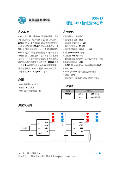
BS0815三通道LED 恒流驱动芯片产品说明BS0815是一颗3通道LED 恒流驱动芯片,内建灰阶脉冲调制,输入电源在5V 到18V 之间。
BS0815包括了3个漏极开路的电流沉输出端,可承受18V并提供30mA的高精度电流给每一串LED,3组输出电流统一由一个外置电阻设置。
BS0815提供了单线的数据传输口,输入频率在400kHz 到1.1MHz 之间。
芯片内部自动生成锁存信号,并且提供可降低电磁波干扰和电源杂波的输出通道电流错位处理方式。
BS0815提供输出电流响应。
BS0815提供SOP8封装型式,工作环境为-40°C 到+85°C 之间。
一般值1%的通道电流输出精度以及快速的管/LED 网屏 工程 ·电流精度:通道间±应用·LED 数码·全彩LED 点光源2012年5月28日版本0.5 BriteStar ·LED 装饰照明/亮化典型应用图芯片特色·单线驱动,恒流模式 ·最大输出电流:30mA ·最大输出承受电压:18V ·芯片工作电压:5V-18V·串行数据频率:400kHz-1.1MHz ·采用Manchester 编码 ·12bits PWM 灰阶调制·数据输出端内建缓冲,支持长串应用,单线级联最大像素点:1024·具PWM 自由运行能力,画面刷新率达550Hz ·ESD:3kV·-40C 到+85C 的环境温度操作范围 ·封装:SOP8±1%,芯片间6% 下单信息±编号 封装信息SOP8 颗/条 100BS0815SOP85000颗/盘三通道LED 恒流驱动器 版本:V0.5 Page 2功能方框图SDOIRVCC GNDSDI脚位图(SOP8)OUT1 VCCOUT2 IROUT3 SDOSDIGND脚位说明Pin名 类型 功能VCC P 芯片电源GND P 芯片地SDI IN 数据输入SDO OUT 数据输出OUT1、OUT2、OUT3 OUT 恒流输出,外接LEDIR IN 外挂输出电阻,调整输出电流三通道LED恒流驱动器 版本:V0.5 Page 3输入输出等效电路1 SDI端2 SDO端3 OUT1~3端三通道LED恒流驱动器 版本:V0.5 Page 4三通道LED 恒流驱动器 版本:V0.5 Page 5最大工作范围特性 代表符号 最大工作范围单位 电源电压 VCC 18 V 输入逻辑电压 SDI -0.5~VDD+0.5V 输出端最大电流 I OUT30 mA 输出端耐受电压 V DS 18 V 接地端电流 I GND 100 mA 数据传输频率范围F DATA 0.4~1.1 MHz工作温度 T OP -40~85 o C 存储温度 T stg -55~150oCESDHBM3kV(1)操作在这些规定值之上也许会造成组件永久的损伤,在绝对的最大条件之下延长操作期限也许会降低组件的可靠性,这些仅是部分的规定值,并且不支持在规格之外的其它条件的功能操作。
如韵电子CONSONANCE1A镍氢电池充电管理集成电路CN3085概述:CN3085是一款可以对镍氢电池进行充电管理的芯片,可以对单节至四节镍氢电池进行充电管理。
该器件内部包括功率晶体管,不需要外部的电流检测电阻和阻流二极管。
CN3085只需要极少的外围元器件,非常适用于便携式产品。
热调制电路可以在器件的功耗比较大或者环境温度比较高的时候将芯片温度控制在安全范围内。
芯片内部集成有高精度电压比较器,可以精确设置恒流充电终止电压。
CN3085充电电流可以通过一个外部电阻设置。
当输入电压掉电时,CN3085自动进入低功耗的睡眠模式,此时电池的电流消耗小于3微安。
其它功能包括输入电压过低锁存,电池低电压时涓流充电,自动再充电,恒流充电,维持充电(定时),电池温度监测以及状态指示等功能。
CN3085采用散热增强型的8管脚小外形封装(SOP8)。
应用:●移动电话●数码相机●电子词典●便携式设备●镍氢电池充电的应用特点:●片内功率晶体管●电压精度1%●在电池电压较低时采用涓流充电●用户可设置的充电电流达1A●采用恒流/恒温模式充电,既可以使充电电流最大化,又可以防止芯片过热●电源电压掉电时自动进入低功耗的睡眠模式●状态指示输出可驱动LED或与单片机接口●维持(定时)充电●自动再充电●电池温度监测功能●封装形式SOP8●产品无铅,满足rohs指令,无卤素管脚排列:典型应用电路:输入电源图1 典型应用电路订购信息:器件型号封装形式工作环境温度包装CN3085 SOP8 -40℃到 85℃盘装,2500片/盘功能框图:图2 功能框图管脚功能描述序号名称功能描述1 TEMP电池温度监测输入端。
将TEMP 管脚接到电池的NTC 传感器的输出端。
如果TEMP 管脚的电压小于输入电压的45%或者大于输入电压的80%,意味着电池温度过低或过高,则充电将被暂停,表示进入电池故障状态。
如果TEMP 在输入电压的45%和80%之间,则电池故障状态将被清除,充电将继续。
rs485的MAX3082芯⽚介绍MAX3082芯⽚介绍RS-485是⼀种基于差分信号传送的串⾏通信链路层协议。
它解决了RS-232协议传输距离太近(15m)的缺陷,是⼯业上⼴泛采⽤的较长距离数据通信链路层协议。
RS-485收发器市场上的种类很多,MAX3082是其中最经常⽤到的⼀种。
MAX3082只适⽤于半双⼯通信,即同⼀时刻线路上只能进⾏数据的接收或发送它允许将主系统的RS-232接⼝的通信电缆长度延长⾄RS-485总线的 1200⽶的长度,并可以同时在总线上挂接若⼲个⼦系统,从⽽能够构成⼀个上位机可以同时控制若⼲个下位机的分布式控制系统。
MAX3082是具有给来⾃通信总线上的信号故障提供⾃动保护的RS-485收发器。
它有1个带3态输出的差分驱动器和1个带3态输⼊的差分接收器。
1/8单位负载的接收器输⼊阻抗,允许多达256个收发器接⼊总线。
在5V供电电源下数据传输速率可达115Kb/s。
当接收器输⼊为短路、开路或空闲时,真正的失效保护使接收器输出逻辑为⾼电平。
采⽤8引脚的SO型和DIP型封装并具有⼯业级产品的⼯作温度范围。
管脚图及主要引脚介绍MAX3082共有8个管脚其管脚排列如图3.4所⽰各管脚功能如下:RO:接收数据的TTL电平输出端;RE:接收允许端低电平有效;DE:发送允许端⾼电平有效;DI:发送数据的TTL电平输⼊端;A:485差分信号的正向端;B:485差分信号的反向端;VCC:电源端;GND:接地端。
图3.4 MAX3082管脚图系统中的作⽤及接线由于RS-485总线使⽤⼀对双绞线传送差分信号,属半双⼯通信,所以应⽤时需要进⾏接收和发送状态的转换。
在⽤MAX3082进⾏RS-485电路设计中,通常将RE和DE短接,⽤1根信号线来控制,这样可以保证收发的正常切换。
MAX3082通常处于接收状态。
当要发送数据时,由程序控制DE变为⾼电平,然后UART 单元发送数据,数据发送完毕后,程序再控制DE变为低电平,使MAX3082转换到数据接收状态。
第一部分RS232/485/422通信模块说明黑金AN3845模块专门为工业现场应用设计的RS232/485/422通信模块。
它包含一路RS232接口,2路RS485和2路RS422通信接口。
配合开发板实现RS232、485和422的数据远程传输和通信。
RS232、485和422接口分别采用MAX3232、MAX3485和MAX3490芯片作为电平转换芯片。
模块留有一个40针的排母用于连接开发板,RS232接口为一个标准的DB9串口公座,通过串口线直接连接电脑或者其他设备;RS485和RS422接口采用接线端子跟外部连接,超远距离传输可达上千米,另外RS485和RS422接口部分带有正负15KV的ESD 防护功能。
AN3845模块实物照片如下:AN3845通信模块正面图1.1 AN3485模块的参数说明以下为AN3485通信模块的详细参数:RS232接口●一路标准的DB9公座串行接口;●使用MAX3232作为RS232和TTL电平的转换;●传输率高达120Kbps数据通讯速率RS485接口●两路RS485接口,采用3线的接线端子;●使用MAX3485作为RS485和TTL的电平转换;●工业级设计,抗干扰能力超强,同时采用有效的防雷设计;●具有120欧匹配电阻,插上跳线帽即可使能匹配电阻,长距离传输时建议短接。
●支持多机通讯,允许接在最多128个设备的总线上●传输率高达500Kbps数据通讯速率。
RS422接口●两路RS422接口,采用5线的接线端子;●使用MAX3490作为RS422和TTL的电平转换;●工业级设计,抗干扰能力超强,同时采用有效的防雷设计;●具有120欧匹配电阻,插上跳线帽即可使能匹配电阻,长距离传输时建议短接。
●支持多机通讯,允许接在最多128个设备的总线上●传输率高达500Kbps数据通讯速率。
1.2 AN3485模块尺寸AN3485通信模块尺寸图第二部分模块功能说明2.1 RS232电路设计AN3485模块的RS232接口采用MAX3232芯片实现RS232和+3.3V TTL 电平的转换。