TC1005 BOM(1)
- 格式:xls
- 大小:29.00 KB
- 文档页数:1


DC1705A-BD ESCRIPTIONUltralow Noise and Spurious Integer-N Frequency Synthesizer with Integrated VCODC1705A features the L TC®6946, an ultralow noise and spurious integer-N frequency synthesizer with integrated VCO. The VCO uses no external components and is inter-nally calibrated without external system support. There are three versions of the DC1705A, one for each version of the L TC6946. The DC1705A-A contains the L TC6946-1, the DC1705A-B incorporates the L TC6946-2 and DC1705A-C uses the L TC6946-3.Each DC1705A provides 50Ω SMA connectors for the reference frequency input, f REF, the reference output buffer (REF OUT), and the differential RF output (RF+ and RF–).A DC590 USB serial controller board is used for SPI com-munication with the L TC6946, controlled by the supplied PLLWizard™ software.Design files for this circuit board are available at /demoL, L T, L TC, L TM, Linear Technology and the Linear logo are registered trademarks and PLLWizard and QuikEval are trademarks of Linear Technology Corporation. All other trademarks are the property of their respective owners.Figure 1. Proper Measurement Equipment Setup1dc1705afaDEMO MANUAL DC1705APARAMETER INPUT OR OUTPUT PHYSICAL LOCATION DETAILS3.3V Power Supply Input 3.3V and GND Banana Jacks Low Noise and Spur-Free 3.3V, 115mA5V Power Supply Input5V and GND Banana Jacks Low Noise and Spur-Free 5V, 45mAREF+ IN, Reference Frequency Input J1 SMA Connector Low Noise 10MHz or 100MHz*, 6dBm into 50Ω(Note 1)REF OUT, Buffered Reference Output J3 SMA Connector Frequency = f REF, 0dBmRF+ and RF–T wo Outputs J4 and J5 SMA Connectors Frequency: 900MHz*, Power: 0dBm, FrequencyRange: Depends on the version of the L TC6946device – refer to Table 1, Step Size: 200kHz* Loop Bandwidth–Set by Loop Filter Component Values47kHz** These frequencies are for the DC1705A pllset files included with PLLWizard.Note 1: A low noise 10MHz or 100MHz reference frequency, such as the Wenzel 501-04608A or 501-04516D OCXO, is recommended. If using a different frequency, make sure to update the f REF and R_DIV boxes under the System tab in PLLWizard so that f PFD is still 1MHz. For example, if a 20MHz clock is used, f REF should be changed to 20MHz and R_DIV to 20. REF BST and FIL T under the System tab in PLLWizard might need to be changed if the reference frequency and/or power is different than what is recommended in the table above. More information can be found in the LTC6946 data sheet.Table 1. DC1705A Options and Frequency RangesASSEMBL Y VERSION PART NUMBER VCO FREQUENCY RANGE (GHz)OUTPUT DIVIDER SETTINGSDC1705A-A L TC6946IUFD-1 2.240 to 3.740Integers 1 through 6DC1705A-B L TC6946IUFD-2 3.080 to 4.910Integers 1 through 6DC1705A-C L TC6946IUFD-3 3.840 to 5.790Integers 1 through 6T YPICAL DC1705A REQUIREMENTS AND CHARACTERISTICSQ UICK START PROCEDUREThe DC590 and PLLWizard application are required to control the DC1705A through a personal computer (PC). DC590 ConfigurationThe DC590’s QuikEval™ drivers must be installed before the DC590 will be able to communicate with the L TC6946. To configure the DC590, follow the procedure below, start-ing with step 1. If you have already installed the DC590 software previously, skip to step 5.Note: Once the QuikEval software is installed, the applica-tion does not need to be executed to run PLLWizard or to control the DC1705A.1. Do Not plug in the DC590 before running the installation program.2. Download the QuikEval installation program from /software.3. Run the QuikEval installation program and follow the on-screen instructions. More detailed installation infor-mation may be found in the DC590’s Quick Start guide.4. Exit the QuikEval program once the installation is com-plete, as it is not needed to run the PLLWizard software.5. Place the DC590 jumpers in the following positions: JP4EE Must be in the “EN” position.JP5ISO ”ON” must be selected.JP5SW ”ON” must be selected.JP6VCCIO “3.3V” must be selected. This sets the SPI port to 3.3V operation.6. Connect the DC590 to one of your computer’s USB ports with the included USB cable.2dc1705afaDEMO MANUAL DC1705AFigure 2. DC590 Jumper LocationsQUICK START PROCEDUREPLLWizard InstallationThe PLLWizard software is used to communicate with the L TC6946 synthesizer. It uses the DC590 to translate between USB and SPI-compatible serial communications formats. It also includes advanced PLL design and simula-tion capabilities. The following are the PLLWizard system requirements:• Windows Operating System: Windows XP, Windows 2003 Server, Windows Vista, Windows 7• Microsoft .NET 2.0 or later• Windows Installer 3.1 or later• Linear Technology’s QuikEval and DC590 hardware Microsoft .NETYou must have Microsoft .NET 2.0 or later installed on your computer. PLLWizard will not run without it. Note that with Windows Vista and Windows 7 have at least version 3.5 pre-installed.To manually determine your version of .NET using Win-dows XP, click Start Menu→Settings→Control Panel →Add or Remove Programs.Depending upon your .NET version, choose one of two PLLWizard setup programs, downloaded from /software.3dc1705afa4dc1705afaDEMO MANUAL DC1705A QUICK START PROCEDUREFigure 3. PLLWizard ScreenshotEither setup program will automatically install Microsoft .NET if a compatible .NET version is not found. But, the installation source depends upon which file you down-loaded from Linear Technology’s website. You should pick one of the following two choices, depending upon your version of .NET .Table 2. PLLWizard Installation FileFILE.NET 2.0 SOURCEPLLWizardSetup.exe Latest Version Downloaded from Microsoft PLLWizardSetup_net20.exe2.0 SP2 Included (Much Larger File Size)• Choose PLLWizardSetup if you have .NET 2.0 or later , have Windows Vista or Windows 7, or if you have less than .NET 2.0 but want the latest .NET installed.• Choose PLLWizardSetup_net20 if you have less than .NET 2.0, and want faster installation (no additional Microsoft downloads are needed, but the file size is much larger).The setup file will verify and/or install Microsoft .NET and install PLLWizard. Refer to the Help menu for softwareoperation.DEMO MANUAL DC1705A QUICK START PROCEDUREDC1705A Configuration1. Connect an appropriate reference frequency source (at J1) and signal analyzers (at J4 and/or J5) using the SMA connectors (see Figure 1 and the Typical DC1705A Requirements and Characteristics table).2. Choose the MUTE jumper setting: JP1 - GND/3.3V MUTE position. Select GND to mute the RF output, 3.3V to un-mute.3. Connect the GND, 3.3V and 5V banana jacks to a power supply and apply power (see Figure 1 and the Typical DC1705A Requirements and Characteristics table).4. Connect the DC590 to the DC1705A with the provided ribbon cable.5. Run the PLLWizard application.6. In PLLWizard, click File → Load Settings and point to the appropriate pllset file. For example, if you are using a 10MHz reference with a DC1705A-B to evaluate the L TC6946-2, load the “DC1705A-B (L TC6946-2) 10MHz Ref.pllset” file found in the PLLWizard installation direc-tory (typically Program Files → L TC → PLLWizard →Set Files).The red LED on DC1705A should turn on indicating that the loop is locked at 900MHz.You can then change the values of N_DIV and/or O_DIV in PLLWizard to change the output frequency.T roubleshootingIf the red LED does not illuminate, follow the instructions below:1. Verify that you are able to communicate with the DC1705A. The bottom status line in PLLWizard should read “L TC6946” and “Comm Enabled.” Refer to PLL-Wizard’s T roubleshoot and Help if not.2. Verify that the3.3V and 5V have the correct voltages on them and that the reference frequency is applied to the REF+ IN SMA input.If the red LED is on but you cannot detect an RF output, make sure jumper JP1 is at the 3.3V position. Run Help →T roubleshoot in PLLWizard if the problem is not resolved. DC1705A ReconfigurationYou can redesign the frequency plan of the DC1705A using PLLWizard. You can change the loop filter components as found using PLLWizard by reinstalling the loop filter components shown in Figure 4.Figure 4. DC1705A Components and Connections5dc1705afaDEMO MANUAL DC1705AP ARTS LISTITEM QTY REFERENCE PART DESCRIPTION MANUFACTURER/PART NUMBERDC1705A General BOM11CI1 Capacitor, X7R 0.022μF 50V 5% 0603AVX 06035C223JAT2A21CI2Capacitor, COG 6800pF 50V 5% 0805Murata GRM2195C1H682JA01D31CP Capacitor, COG 2700pF 50V 5% 0603Murata GRM1885C1H272JA01D44C1, C8, C9, C18Capacitor, X7R, 1μF, 16V, 10%, 0805TDK, C2012X7R1C105K52C2, C10Capacitor, Tantalum, 330μF, 10V, 10%, 7343AVX, TPME337K010R003562C6, C11Capacitor, X7R, 470pF, 50V, 10%, 0402AVX, 04025C471KAT2ACapacitor, X7R, 0.01μF, 16V, 10%, 0402AVX, 0402YC103KAT2A 74C7, C12, C15,C198C13, C14, C17,Capacitor, X5R, 0.1μF, 10V, 10%, 0402TDK, C1005X5R1A104KC22, C23,8C24, C25, C2691C16Capacitor, X7R, 2.2μF, 16V, 10%, 0805TDK, C2012X7R1C225K102C20, C21Capacitor, NPO, 100pF, 50V, 5%, 0402TDK, C1005C0G1H101J111D1LED, Red Panasonic, LN1251CTR124E1, E2, E5, E8Jack, Banana Keystone, 575-4131E3Turret, Testpoint, 2501 Mill-Max, 2501-2-00-80-00-00-07-0141JP1Headers, 3 Pins 2mm Ctrs.Samtec TMM-103-02-L-S151XJP1Shunt, 2mm Ctrs.Samtec 2SN-BK-G164J1, J3, J4, J5Connector, SMA 50Ω EDGE-LAUNCH E. F. Johnson, 142-0701-851171J2Connector, Header, 14-Pin, 2mm Molex, 87831-1420182L1, L2Inductor, Chip, 68nH, ±5%, 0402 Coilcraft, 0402 HPH-68NXJL191RZ Resistor, Chip, 453 1/10W 1% 0603NIC, NRC06F4530TRF201R1Resistor, Chip, 51.1Ω, 1/16W, 1% 0402NIC, NRC04F51R1TRF211R3Resistor, Chip, 330Ω, 1/16W, 1% 0402NIC, NRC04F3300TRF221R4Resistor, Chip, 15Ω, 1/16W, 1% 0402NIC, NRC04F15R0TRF234R5, R6, R7, R13Resistor, Chip, 200k, 1/16W, 1% 0402NIC, NRC04F2003TRF242R8, R9Resistor, Chip, 4.99k, 1/16W, 1% 0402NIC, NRC04F4991TRF253R10, R11, R12Resistor, Chip, 100Ω 1/16W, 5%, 0402NIC, NRC04J101TRF262U2, U3IC, Dual Buffer SC-70 6-Lead Fairchild Semi. NC7WZ17P6X271U4 IC, Dual T ransceiver SC-70 6-Lead NXP 74LVC1T45GW284 4 Corners Standoff, Nylon, 0.5, 1/2"Keystone, 8833 (SNAP ON)DC1705A-A11DC1705A General BOM DC1705A21U1IC Synthesizer QFN-28 4mm × 5mm Linear Technology Corporation, L TC6946IUFD-1DC1705A-B11DC1705A General BOM DC1705A21U1IC Synthesizer QFN-28 4mm × 5mm Linear Technology Corporation, L TC6946IUFD-2DC1705A-C11DC1705A General BOM DC1705A21U1IC Synthesizer QFN-28 4mm × 5mm Linear Technology Corporation, L TC6946IUFD-36dc1705afa7dc1705afaDEMO MANUAL DC1705ASCHEMATIC DIAGRAM8dc1705afaDEMO MANUAL DC1705A SCHEMATIC DIAGRAMNote: The buffers shown on sheet 2 of 2 of the schematic are used to protect the L TC6946 when communicating to it starts before powering it up. There is no need for such circuitry if the SPI bus is not active before powering up the LTC6946.9dc1705afaDEMO MANUAL DC1705AInformation furnished by Linear Technology Corporation is believed to be accurate and reliable.However , no responsibility is assumed for its use. Linear Technology Corporation makes no representa-tion that the interconnection of its circuits as described herein will not infringe on existing patent rights.L AYOUT The top metal layer of the DC1705A is shown here as an example of good PCB layout for the L TC6946.10dc1705afa DEMO MANUAL DC1705ALinear Technology Corporation 1630 McCarthy Blvd., Milpitas, CA 95035-7417(408) 432-1900 ● FAX: (408) 434-0507 ● www.linear .com © LINEAR TECHNOLOGY CORPORA TION 2011LT 1211 REV A • PRINTED IN USADEMONSTRATION BOARD IMPORTANT NOTICELinear Technology Corporation (L TC) provides the enclosed product(s) under the following AS IS conditions:This demonstration board (DEMO BOARD) kit being sold or provided by Linear Technology is intended for use for ENGINEERING DEVELOPMENT OR EVALUATION PURPOSES ONL Y and is not provided by L TC for commercial use. As such, the DEMO BOARD herein may not be complete in terms of required design-, marketing-, and/or manufacturing-related protective considerations, including but not limited to product safety measures typically found in finished commercial goods. As a prototype, this product does not fall within the scope of the European Union directive on electromagnetic compatibility and therefore may or may not meet the technical requirements of the directive, or other regulations.If this evaluation kit does not meet the specifications recited in the DEMO BOARD manual the kit may be returned within 30 days from the date of delivery for a full refund. THE FOREGOING WARRANTY IS THE EXCLUSIVE WARRANTY MADE BY THE SELLER TO BUYER AND IS IN LIEU OF ALL OTHER WARRANTIES, EXPRESSED, IMPLIED, OR STATUTORY, INCLUDING ANY WARRANTY OF MERCHANTABILITY OR FITNESS FOR ANY PARTICULAR PURPOSE. EXCEPT TO THE EXTENT OF THIS INDEMNITY, NEITHER PARTY SHALL BE LIABLE TO THE OTHER FOR ANY INDIRECT , SPECIAL, INCIDENTAL, OR CONSEQUENTIAL DAMAGES.The user assumes all responsibility and liability for proper and safe handling of the goods. Further , the user releases L TC from all claims arising from the handling or use of the goods. Due to the open construction of the product, it is the user’s responsibility to take any and all appropriate precautions with regard to electrostatic discharge. Also be aware that the products herein may not be regulatory compliant or agency certified (FCC, UL, CE, etc.).No License is granted under any patent right or other intellectual property whatsoever. L TC assumes no liability for applications assistance, customer product design, software performance, or infringement of patents or any other intellectual property rights of any kind.L TC currently services a variety of customers for products around the world, and therefore this transaction is not exclusive .Please read the DEMO BOARD manual prior to handling the product . Persons handling this product must have electronics training and observe good laboratory practice standards. Common sense is encouraged .This notice contains important safety information about temperatures and voltages. For further safety concerns, please contact a L TC applica-tion engineer .Mailing Address:Linear Technology1630 McCarthy Blvd.Milpitas, CA 95035Copyright © 2004, Linear Technology CorporationDC1705A-B。

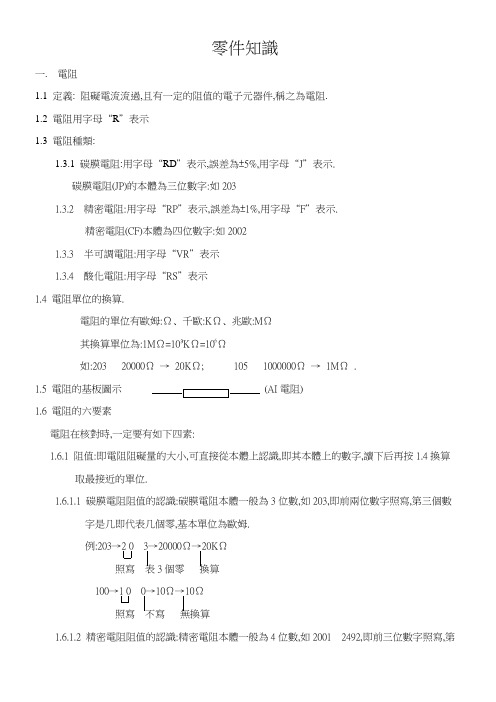
零件知識一. 電阻1.1 定義: 阻礙電流流過,且有一定的阻值的電子元器件,稱之為電阻.1.2 電阻用字母“R”表示1.3 電阻種類:1.3.1 碳膜電阻:用字母“RD”表示,誤差為±5%,用字母“J”表示.碳膜電阻(JP)的本體為三位數字:如2031.3.2 精密電阻:用字母“RP”表示,誤差為±1%,用字母“F”表示.精密電阻(CF)本體為四位數字:如20021.3.3 半可調電阻:用字母“VR”表示1.3.4 酸化電阻:用字母“RS”表示1.4 電阻單位的換算.電阻的單位有歐姆:Ω﹑千歐:KΩ﹑兆歐:MΩ其換算單位為:1MΩ=10³KΩ=106Ω如:203 20000Ω→20KΩ; 105 1000000Ω→1MΩ.1.5 電阻的基板圖示(AI電阻)1.6 電阻的六要素電阻在核對時,一定要有如下四素:1.6.1 阻值:即電阻阻礙量的大小,可直接從本體上認識,即其本體上的數字,讀下后再按1.4換算取最接近的單位.1.6.1.1 碳膜電阻阻值的認識:碳膜電阻本體一般為3位數,如203,即前兩位數字照寫,第三個數字是几即代表几個零,基本單位為歐姆.例:203→2 0 3→20000Ω→20KΩ照寫表3個零換算100→1 0 0→10Ω→10Ω照寫不寫無換算1.6.1.2 精密電阻阻值的認識:精密電阻本體一般為4位數,如2001 2492,即前三位數字照寫,第四個數字是几即代表几個零,基本單位也為歐姆.例:2001→200 1→2000Ω→2KΩ照寫表一個零2492→249 2→24900Ω→24.9KΩ照寫表二個零換算1.6.1.3 其它阻值的認識:有的電阻因體積太小或其它原因無法將規格印在零件本體,即需萬用表測量並核對原料盤規格方可.1.6.1.4 電阻阻值單位的選擇電阻國際單位為歐姆(Ω),常用單位為千歐(KΩ),如何用一個正確的單位來表明阻值呢?一般的,以歐姆為單位的電阻,其數字顯示不大于1000,如:不能講203為兩萬歐姆;以KΩ為單位的阻值其數字范圍為1∠@∠1000 如:不能講101為零點一千歐或105為一仟千歐.以KΩ為單位的電阻其數字不得小于1.1.6.2 誤差電阻在制造過程中其阻值不可能一模一樣,我們將電阻的實測值與定值之間的差異稱之為誤差,通常電阻誤差有F及J兩種. F=±1% J=±5% 我們一般稱±1%(F)誤差之電阻為精密電阻,±5%(J)誤差之電阻為碳膜電阻.1.6.2.1 誤差上限:其計處算分式為:定值+定值×(+誤差值)例: 203的誤差上限為: 203→20K→20K+20K*(+5%)=21K1.6.2.2 誤差下限:其計算公式為:定值+定值×(-誤差值)例:203的誤差下限為:203→20K→20K+20K×(-5%)=19K即為本體標示為203之電阻其測量值容許范圍為19K-21K之間.1.6.3 尺寸電阻的尺寸大小在SMT的置件過程中影響極大,一般地電阻大小分公制及英制兩種講法,其本質大小一樣.例:公制:1005表示電阻的長為1.0mm,寬為0.5mm,同理1608 2012等都如此.英制:0402表示電阻的長為0.04in,寬為0.02in,同理0603 0805等都如此.公英制的互換關系為:1in=25.4mm1.6.4 功率電阻阻礙電流要做功,其功率的大小直接關系產品的信耐度,一般地,電阻的功率與其制选材質﹑工藝及體積的關系,體積越大之電阻其功率越大,阻值越大.如:0805的電阻較0603而言更能增大阻值及功率,一般習慣稱0603為1/16W電阻,0805為1/8W電阻,1206為1/4W電阻,但此稱呼不絕對,如:0805的電阻亦有可能做1/4W功,且功率只可稱電阻而不可稱呼電容,如:1206大小的電容稱之為1/4W的電容即是錯誤的.二. 電容(CAPACITY)2.1 定義:在電子產品中起著濾波,消除雜質作用的元器件.2.2 電容用字母“C”表示.2.3 電容單位:通常有“F”法拉﹑“UF”微法﹑“NF”納法﹑“FP”皮法其換算單位為:1F=106UF=109NF=1012F1UF=10-6F=106PF 1PF=10-6UF=10-12F2.4 電容種類2.4.1 陶瓷電容:用字母“CC”表示,無極性.2.4.2 膽質電容:用字母“TC”表示,有方向,有極性.2.4.3 電解電容:用字母“EC”表示,有方向,有極性.2.4.4 塑膠電容:用字母“BC”表示,無極性.2.4.5 半可調電容:用字母“VC”表示,無極性.(Trimmer Cap)2.4.6 麥拉電容:用字母“MC”表示,無極性.2.5 電容的誤差:C:±0.25PF D:±0.5PFH:±3% J:±5%K:±10% X:±15%Z:-20%±80% M:±20%P:±100%-0%通有所用之誤差為:J:±5%, K: ±10%, M:±20%, Z:±80%-20%2.6 電容的耐壓:16V 25V 50V 100V 200V 500V 1000V2.7 材質分為:(亦稱耐溫)X7R Y5V Z5U NPO N330(特殊材質)其中X7R材質最好.其耐溫系數為:Y5V:-25℃+85℃X7R:-55℃+125℃Z5U:+10℃+85℃NPO:0℃±60℃如:104Z/25V NPO 0.01UF/25V NPO104表示:容值;Z表示:誤差;25V表示:耐壓;NPO表示:材質2.8 基板圖示“C”2.9 電容的六要素電容在材料核對時一定注意以下六要素:2.9.1 容值:可測量或從料盤上認知,其計算方法如:1.6.1.1碳膜電阻之計算,但其換算進位不一樣,見2.3.2.9.2 誤差:同電阻的計算誤差上﹑下限.2.9.3 耐壓:電流通過時所承受的壓降值,直接從料盤得知.2.9.4 耐溫:電容所能耐受的溫度范圍而其本身特性不受破壞.2.9.5 大小:如電阻的公﹑英制稱呼,但不能按其大小稱呼“xxw”.2.9.6 極性:電容在電路上的使用其極性很重要,主要識別如:2.4的不同種類電容極性標示不一樣,CC﹑BC﹑VC﹑MC,一般使用時均無極性.EC在本體特殊端為負極,而TC的本體特殊端為正極.三.二極體(DIODE)3.1 定義:起整流穩壓﹑截波或溫度補償等作用的元件.3.2 二極體用字母“D”表示.3.3二極體基本圖為“D”3.4 注意事項:1有方向性,有極性,所有零件本體特殊端為負極.3.4.2 標示在本體上的印碼文字或色環不能錯.3.4.3 體積大小是否與BOM 相吻合.3.4.4 二極體規格可直接看本體標示或資料顯示不用計算.3.5 二極體的分類:整流二極體:DR;開關二極體:DS;積納二極體:DZ;快速恢復二極體:DF;發光二極體:DE;橋堆二極體:DB.四.電晶體(TRANSISTOR)4.1 電晶體用字母“Q ”表示.4.2 有方向,有極性.4.3 其基本圖示為4.4 注意事項 同二極體)五.IC(INTEGRATED CIRCUIT)5.1 IC 用字母“U ”表示,起集成電路的作用,又叫集成塊.5.2 IC 的種類SOIC:兩邊腳外彎; SOJIC:兩邊腳內彎. QFP:四邊腳外彎; PLCC:四邊腳內彎.SOIC SOJIC PLCC5.3 有方向.(一般以圓點方向為準),若一顆IC 有几個圓點,以特殊點為第一只腳.5.4 IC 的規格本體上有印碼數字.六.其它零件:觸動開關:“SW ”;振動器:“Y ”“X ”;線圈:“L ”;電解電容:“EC ”;變壓器:“T ”.。

南京科远自动化集团股份有限公司电子产品BOM编制与维护指导文件编号: KY•KF•A•00-JS-TS 08编制:王素慧审核:乔熹批准:李海康受控状态:受控2011年01月31日发布 2011年01月31日实施电子产品BOM编制与维护指导目录1.目的和范围............................................错误!未定义书签。
2.引用文件..............................................错误!未定义书签。
3.职责..................................................错误!未定义书签。
4.术语..................................................错误!未定义书签。
5.工作程序..............................................错误!未定义书签。
BOM封面................................................ 错误!未定义书签。
BOM修改履历............................................ 错误!未定义书签。
BOM的建立.............................................. 错误!未定义书签。
BOM的维护.............................................. 错误!未定义书签。
6.模板..................................................错误!未定义书签。
1.目的和范围对于科远公司电子产品,技术中心硬件设计人员能够编制出符合要求的BOM并正确的进行维护,确保后续采购、生产过程的正常进行。
2.引用文件无角色职责硬件设计人员负责BOM的编制和维护4.术语1、BOM:Bill of Materials,指材料清单。

XXXX有限责任公司品种名T1005 Tray文件名称T1005出货Tray盘清洁手顺作业标准书一.治工具酒精,无尘布,离子风扇,air gun二.作业流程二:清洁作业1.Tray赃污去除1)拿取tray(sensor来料新tray),去除tray中胶带2)使用无尘布沾酒精进行TRAY正面擦拭.确认不可有残胶及赃污(无法去除刮痕OK)3)无尘布沾酒精进行TRAY背面擦拭. 确认不可有残胶及赃污(无法去除刮痕OK)注:1) tray正面必须擦拭区域如下图一2) tray背面必须擦拭区域如下图二XXXX有限责任公司品种名T1005 Tray文件名称T1005出货Tray盘清洁手顺作业标准书3) 正面放置区及背面擦拭细化部分如上四图:a. 正面放置区:FPC槽由边缘至中间进行擦拭(图正面1) ,放置区下凹处使用无尘布如图作顺时针旋转清洁(图正面2)。
b. 背面擦拭:凸块部分以长边为擦拭方向进行(图背面1) ,下凹部分以从上至下,从左至右方向进行清洁(图背面2)。
XXXX有限责任公司品种名T1005 Tray文件名称T1005出货Tray盘清洁手顺作业标准书2.TRAY 凸棱边清洁1)拿取TRAY使用干净干燥无尘布对TRAY正面放置区棱边进行擦拭,擦拭方式及顺序如下图三,四2)反转TRAY使用干净干燥无尘布对TRAY背面放置区棱边进行擦拭, 擦拭方式及顺序如下图五,六XXXX有限责任公司品种名T1005 Tray文件名称T1005出货Tray盘清洁手顺作业标准书3.A I R G U N吹除1)使用AIR GUN对正面TRAY进行吹除,吹除方式及顺序如下图七2)使用AIR GUN对正面TRAY进行吹除,吹除方式及顺序同正面吹除3)对光检查确认TRAY无未干溶剂水痕4)使用红色记号笔于TRAY正面字模侧进行打点表示,如图八PS:UV工程内周转透明Tray擦拭手顺同二检擦拭手顺,无尘布沾酒精擦拭OK后无须使用干布擦拭&a i r g u n吹除.4.擦拭效果确认如下图:。
1号线AFC系统作业工艺卡汇编_可读1号线AFC系统作业工艺卡汇编目录1号线AFC系统日检作业工艺卡 (5)1号线AFC系统月检作业工艺卡(1/3)--中心主机/数据库 (12)1号线AFC系统月检作业工艺卡(2/3)--中心网络 (25)1号线AFC系统月检作业工艺卡(3/3)--车站数据库 (32)1号线AFC系统年检作业工艺卡 (37)1号线AFC系统专项检查作业工艺卡(1/7)--病毒库更新 (40)1号线AFC系统专项检查作业工艺卡(2/7)--一期设备压数处理 (43)1号线AFC系统专项检查作业工艺卡(3/7)--二期设备压数处理 (49)1号线AFC系统专项检查作业工艺卡(4/7)--一期设备黑名单下发 (55)1号线AFC系统专项检查作业工艺卡(5/7)--一期设备用户参数下发 (58)1号线AFC系统专项检查作业工艺卡(6/7)--一期设备票价参数更新 (63)1号线AFC系统专项检查作业工艺卡(7/7)--一期设备运营点参数下发 (68)1号线AFC系统日检作业工艺卡作业人员必须是AFC系统维护人员;查过程中不得有任何影响设备运行的操作。
证系统的正常运行;意操作命令的使用,本工作只使用查询命令,不能执行有修改操作的是新员工进行操作,必须有老员工进行指导。
检修步骤lnet方式分别登录两台主机,执行以下命令:输入errpt操作系统报错信息;输入date操作系统当前时间,计算与时钟源(DMC 通信机)时间误差; 输入 df -P各文件系统的空间使用情况;(重点关注home,oracle);输入 lsvg rootvgROOTVG 的详细信息(主要查看VG STATE ;STALE PVs 和PPs ); 输入 lsps -a交换使用百分比、空间是活动还是非活动的以及交换空间是否设置为等;输入crs_stat -t各节点资源状态;输入-500f /oracle/product/10.2.0/admin/afc/bdump/alert_afc*Oracle 告警日志,检查是否有报错信息;打开OEM,连接DMC 数据库AFC_DATA 、INDX 、INDX_*、TS_*表空间利用率或增长状态: 打开数据监控软件,开启数据监控车站各类设备数据上传情况:登陆数据库,运行异常交易检查脚本有无扣费为零交易、非法交易等;交易t * from td_fareend where tradedate >= sysdate -1 and asic='0' and tradetype='22' and substr(cardid,1,2) Not 8','21','98','84','85')工卡异常交易t * from td_fareend where tradedate >=sysdate -1 and r(cardid,1,2) = '88' and tradetype <> '11' and tradetype <> and farebasic <> '0'生卡异常交易t * from td_fareendtradedate >=sysdate - 1ubstr(cardid,1,2) in ('05','15','25')radetype = '22'farebasic not00','150','200','250','300','350','400','450','500','550') 值卡异常交易 t * from td_common tradedate >=sysdate - 1 andype not in ('05','15','25','88','98','81','21','84','85')radetype = '22' trademoney not90','285','380','475','570','665','760','855','950','1045') radetypeex<>'2201'程优惠异常交易t * from td_commontradedate >=sysdate - 1ardtype not in ('05','15','25','88','98','81','21','85','84')radetype = '22' trademoney not50','245','340','435','530','625','720','815','910','1005') radetypeex='2201'lnet 方式登陆主机,输入dsmadmc 进入TSM 控制台输入q event * *;数据备份计划任务执行情况。