光耦资料PS2801
- 格式:pdf
- 大小:123.47 KB
- 文档页数:12

kp2801是一款高性能、准谐振式(QR)升压型(Boost)恒压功率因数校正(PFC)控制器。
它具有自适应工作模式,可以在临界导通模式(CRM)和断续导通模式(DCM)之间自动切换,以实现高功率因数(PF)和低输入谐波(THD)的性能。
kp2801具有优化控制算法和输入线电压前馈补偿,可以轻松实现高效率。
同时,它还具有打嗝(Burst)模式,可以在轻载时提高效率并降低系统待机损耗。
此外,kp2801还具有高压启动和供电电路,无须外部供电即可实现快速启动和供电功能。
因此,kp2801对应的元件是一款高性能、准谐振式升压型恒压功率因数校正控制器,适用于宽电压输出电路。
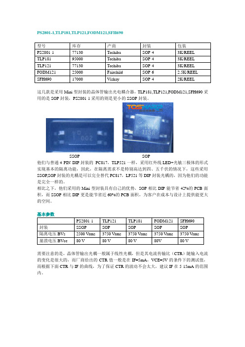
PS2801-1,TLP181,TLP121,FODM121,SFH690型号库存产商封装包装PS2801-1 77130 Toshiba SOP-4 3K/REELTLP181 95000 Toshiba SOP-4 3K/REELTLP121 77130 Toshiba SOP-4 3K/REEL FODM121 25000 Fairchild SOP-6 2.5K/REEL SFH690 17000 Vishay SOP-4 2K/REEL这几款是采用Mini型封装的晶体管输出光电耦合器,TLP181,TLP121,FODM121,SFH690采用的是SOP封装,PS2801-1采用的则是更小的SSOP封装。
SSOP SOP他们与普通4 PIN DIP封装的PC817,TLP521一样,采用红外线LED+光敏三极体的形式实现基本的隔离功能,因此,在隔离需求不是特别高达到四、五千伏的情况下,这些采用SSOP,SOP封装的光耦是可以完全替代PC817,LP521等DIP封装光耦的,因为他们的功能是完全一样的。
相比之下,他们采用的Mini型封装具有自己的优势,SOP相比DIP能节省42%的PCB面积,而SSOP相比DIP更是能节省近60%的PCB面积,为客户在成本与设计上提供能更大的空间。
基本参数PS2801-1 TLP121 TLP181 FODM121 SFH690封装SSOP SOP SOP SOP SOP隔离电压BVs 2500 Vrms 3750 Vrms 3750 Vrms 3750 Vrms 3750 Vrms崩溃电压BVce 80 V 80 V 80 V 80V 80 V需要注意的是,晶体管输出光耦一般属于线性光耦,但是其电流传输比(CTR)随输入电流的变化是很大的,而厂商给出的CTR值一般是在IF=5mA,VCE=5V的条件下的测试值,而根据下面CTR与IF的曲线,为了保证CTR的波动不会太大,建议IF在5-15mA的范围内。

光耦PS2701英⽂数据⼿册DATA SHEETThe information in this document is subject to change without notice.1988Document No. P11306EJ6V0DS00 (6th edition)Date Published December 1997 NS CP (K)Printed in JapanPHOTOCOUPLERPS2701-1,PS2701-2,PS2701-4HIGH ISOLATION VOLTAGE SOP MULTI PHOTOCOUPLERThe mark shows major revised points.NEPOC TMSeries ?DESCRIPTIONThe PS2701-1, PS2701-2, PS2701-4, are optically coupled isolators containing a GaAs light emitting diode and an NPN silicon phototransistor.This package is SOP (Small Outline Package) type and has shield effect to cut off ambient light.It is designed for high density mounting applications.FEATURESHigh isolation voltage (BV = 3 750 Vr.m.s.)SOP (Small Outline Package) typeHigh-speed switching (t r = 3 µs TYP., t f = 5 µs TYP.)Ordering number of taping product (only 1-channel type) : PS2701-1-E3, E4, F3, F4UL approved: File No. E72422 (S) VDE0884 approved (Option)APPLICATIONSHybrid ICMeasuring instruments Power supplyProgrammable logic controllersORDERING INFORMATIONPart Number Package Safety Standard ApprovalPS2701-14-pin SOP Standard products PS2701-28-pin SOP ? UL approvedPS2701-416-pin SOP PS2701-1-V 4-pin SOP VDE0884 approved products (Option)PS2701-2-V 8-pin SOP PS2701-4-V16-pin SOP24.5 MAX.7.0±0.34.41.30.5±0.30.15+0.10–0.05TOP VIEW1. Anode2. Cathode3. Emitter4. Collector43122.00.1±0.12.3 M A X .2.54 1.2 MAX.0.4+0.10–0.05 0.25 MPS2701-29.3 MAX.2.00.1±0.12.3 M A X .2.541.2 MAX.0.4+0.10–0.050.25 MTOP VIEW1234851. 3. Anode2. 4. Cathode 5. 7. Emitter 6. 8. Collector 7.0±0.34.41.30.5±0.30.15+0.10–0.05PS2701-419.46 MAX.TOP VIEW1. 3. 5. 7. Anode2. 4. 6. 8. Cathode 9. 11. 13. 15. Emitter 10. 12. 14. 16. Collector161514131211109123456782.00.1±0.12.3 M A X .2.541.2 MAX.0.4+0.10–0.050.25 M7.0±0.34.41.30.5±0.30.15+0.10–0.05PS2701-1PS2701-2,PS2701-4Diode Forward Current (DC)I F50mAReverse Voltage V R6VPower Dissipation Derating?P D/°C0.8mW/°CPower Dissipation P D80mW/chPeak Forward Current*1I FP1ATransistor Collector to Emitter Voltage V CEO40VEmitter to Collector Voltage V ECO6VCollector Current I C80mA/chPower Dissipation Derating?P C/°C 1.5 1.2mW/°CPower Dissipation P C150120mW/chIsolation Voltage*2BV 3 750Vr.m.s.Operating Ambient Temperature T A–55 to +100°CStorage Temperature T stg–55 to +150°C*1PW = 100 µs, Duty Cycle = 1 %*2AC voltage for 1 minute at T A = 25 °C, RH = 60 % between input and output 34ELECTRICAL CHARACTERISTICS (T A = 25 °C)ParameterSymbol Conditions MIN.TYP.MAX.Unit DiodeForward Voltage V F I F = 5 mA 1.11.4VReverse Current I R V R = 5 V5µA Terminal CapacitanceC t V = 0 V, f = 1 MHz 30pFTransistor Collector to Emitter CurrentI CEO I F = 0 mA, V CE = 40 V 100nA CoupledCurrent Transfer Ratio *1300%Collector Saturation VoltageV CE (sat)I F = 10 mA, I C = 2 mA 0.3V Isolation Resistance R I-O V I-O = 1 kV DC1011Isolation Capacitance C I-O V = 0 V, f = 1 MHz0.4pFRise Time *2t r V CC = 5 V, I C = 2 mA, R L = 100 ?3µsFall Time*2t f5*1CTR rank (only PS2701-1)P: 150 to 300 (%)L: 100 to 300 (%)M: 50 to 150 (%)*2Test circuit for switching timePW = 100 s,Duty cycle = 1/10µPulse inputV CCV OUTR L = 100 ?50 ?I F5TYPICAL CHARACTERISTICS (T A = 25 °C, unless otherwise specified)1005025075255075100Ambient Temperature T A (?C)D i o d e P o w e r D i s s i p a t i o n P D (m W ) DIODE POWER DISSIPATION vs.AMBIENT TEMPERATURE200150100Ambient Temperature T A (?C)T r a n s i s t o r P o w e r D i s s i p a t i o n P C (m W )TRANSISTOR POWER DISSIPATION vs.AMBIENT TEMPERATURE PS2701-11.5 mW/?CPS2701-2,PS2701-41.2 mW/?C50200403010610248Collector to Emitter Voltage V CE (V)C o l l e c t o r C u r r e n t I C (m A )COLLECTOR CURRENT vs.COLLECTOR TO EMITTER VOLTAGEI F = 30 mA20 mA10 mA15 mA5 mA1000.110.01100.61.0 1.4 1.60.8 1.2Forward Voltage V F (V)F o r w a r d C u r r e n t I F (m A ) FORWARD CURRENT vs.FORWARD VOLTAGE+25 ?C 0 ?C –25 ?C –55 ?CT A = +100 ?C+75 ?C +50 ?C10 0000.11001 000101–6004080–40–202060100Ambient Temperature T A (?C)COLLECTOR TO EMITTER DARKD a r k C u r r e n t I CE O (n A )V CE = 40 V24 V 10 V5050.1100.50.220210.20.6 1.00.00.40.8Collector Saturation Voltage V CE (sat) (V)C o l l e c t o r C u r r e n t I C (m A )COLLECTOR CURRENT vs.COLLECTOR SATURATION VOLTAGEI F = 25 mA10 mA 5 mA 2 mA 1 mA61.20.60.00.81.00.40.202550100–50–2575Ambient Temperature T A (?C)NORMALIZED CURRENT TRANSFER RATIO vs. AMBIENT TEMPERATURE N o r m a l i z e d C u r r e n t T r a n s f e r R a t i o C T RNormalized to 1.0 at T A = 25 ?C,I F = 5 mA, V CE = 5 V,,,,,,,,,,,,,,,,,,,,,,,,,,,,,,,,,,,,,,,,,,,,,,,,2001000.050.55500.1110Forward Current I F (mA)C u r r e n t T r a n s f e r R a t i o C T R (%)CURRENT TRANSFER RATIO vs.FORWARD CURRENTV CE = 5 VLoad Resistance R L (?)SWITCHING TIME vs.LOAD RESISTANCES w i t c h i n g T i m e t ( s )µV CC = 5 V,I C = 2 mA 1000.50.150105150200 1 k 2 k100500Load Resistance R L (?)SWITCHING TIME vs.LOAD RESISTANCES w i t c h i n g T i m e t ( s )µt on t offt dt s1.20.40.00.80.60.21.020500510200250100Frequency f (kHz)N o r m a l i z e d G a i n G VFREQUENCY RESPONSER L = 1 k ?510 ?300 ?100 ?1.21.00.00.40.20.80.61021031104105106Time (Hr)LONG TERM CTR DEGRADATIONC T R (R e l a t i v e V a l u e )I F = 1 mA, T A = 25 ?C I F = 5 mA, T A = 25 ?C I F = 20 mA, T A = 25 ?C I F = 20 mA, T A = 60 ?C I F = 5 mA, V CC = 5 V, CTR = 169 %1 0001 k 10 k 50 k 500 5 k 100 k t f t st r t dRemark The measurement of TYPICAL CHARACTERISTICS are only for reference, not guaranteed. 7TAPING SPECIFICATIONS (in millimeters)Outline and Dimensions (Tape)1.55±0.12.0±0.14.0±0.11.55±0.11.75±0.15.5±0.112.0±0.24.6±0.12.4±0.17.4±0.10.38.0±0.1Tape DirectionPS2701-1-E3PS2701-1-F3PS2701-1-E4PS2701-1-F4Outline and Dimensions (Reel)Packing: PS2701-1-E3, E4 900 pcs/reelPS2701-1-F3, F4 3 500 pcs/reel1.5±0.51202.0±0.56.0±121.0±0.8φ6012.4+2.0–0.018.4 MAX.66φ13.0±0.5φP S 2701-1-E 3, E 4: 178P S 2701-1-F 3, F 4: 330φφ8RECOMMENDED SOLDERING CONDITIONS(1) Infrared reflow soldering ?Peak reflow temperature235 °C (package surface temperature)?Time of temperature higher than 210 °C 30 seconds or less ?Number of reflows ThreeFluxRosin flux containing small amount of chlorine (The flux with a maximum chlorine content of 0.2 Wt % is recommended.)60 to 90 s (preheating)210 ?C120 to 160 ?CP a c k a g e S u r f a c e T e m p e r a t u r e T (?C )Time (s)(heating)to 10 sto 30 s235 ?C (peak temperature)Recommended Temperature Profile of Infrared ReflowPeak temperature 235 ?C or belowCaution Please avoid to removed the residual flux by water after the first reflow processes.(2) Dip soldering ?Temperature 260 °C or below (molten solder temperature)?Time10 seconds or less ?Number of times OneFluxRosin flux containing small amount of chlorine (The flux with a maximum chlorine content of 0.2 Wt % is recommended.) SPECIFICATION OF VDE MARKS LICENSE DOCUMENT (VDE0884)Parameter Symbol Speck Unit Application classification (DIN VDE 0109)for rated line voltages ≤ 300 Vr.m.s.IVfor rated line voltages ≤ 600 Vr.m.s.IIIClimatic test class (DIN IEC 68 Teil 1/09.80)55/100/21Dielectric strengthMaximum operating isolation voltage U IORM710V peakTest voltage (partial discharge test, procedure a for type test and random test)U pr850V peakU pr = 1.2 × U IORM, P d < 5 pCU pr = 1.6 × U IORM, P d < 5 pCHighest permissible overvoltage U TR 6 000V peakDegree of pollution (DIN VDE 0109)2Clearance distance> 5mm Creepage distance> 5mm Comparative tracking index (DIN IEC 112/VDE 0303 part 1)CTI175 Material group (DIN VDE 0109)III aStorage temperature range T stg–55 to +150°C Operating temperature range T A–55 to +100°CIsolation resistance, minimum valueV IO = 500 V dc at T A = 25 °C Ris MIN.1012?V IO = 500 V dc at T A MAX. at least 100 °C Ris MIN.1011?Safety maximum ratings(maximum permissible in case of fault, see thermal derating curve)Package temperature Tsi150°CCurrent (input current I F, Psi = 0)Isi200mAPower (output or total power dissipation)Psi300mWIsolation resistanceV IO = 500 V dc at T A = 175 °C (Tsi)Ris MIN.109?9[MEMO] 10[MEMO]11CAUTIONWithin this device there exists GaAs (Gallium Arsenide) material which is aharmful substance if ingested. Please do not under any circumstances break thehermetic seal.NEPOC is a trademark of NEC Corporation.No part of this document may be copied or reproduced in any form or by any means without the prior written consent of NEC Corporation. NEC Corporation assumes no responsibility for any errors which may appear in this document.NEC Corporation does not assume any liability for infringement of patents, copyrights or other intellectual property rights of third parties by or arising from use of a device described herein or any other liability arising from use of such device. No license, either express, implied or otherwise, is granted under any patents, copyrights or other intellectual property rights of NEC Corporation or others.While NEC Corporation has been making continuous effort to enhance the reliability of its semiconductor devices, the possibility of defects cannot be eliminated entirely. To minimize risks of damage or injury to persons or property arising from a defect in an NEC semiconductor device, customers must incorporate sufficient safety measures in its design, such as redundancy, fire-containment, and anti-failure features.NEC devices are classified into the following three quality grades:"Standard", "Special", and "Specific". The Specific quality grade applies only to devices developed based on a customer designated "quality assurance program" for a specific application. The recommended applications of a device depend on its quality grade, as indicated below. Customers must check the quality grade of each device before using it in a particular application.Standard: Computers, office equipment, communications equipment, test and measurement equipment, audio and visual equipment, home electronic appliances, machine tools, personal electronicequipment and industrial robotsSpecial: Transportation equipment (automobiles, trains, ships, etc.), traffic control systems, anti-disaster systems, anti-crime systems, safety equipment and medical equipment (not specifically designedfor life support)Specific: Aircrafts, aerospace equipment, submersible repeaters, nuclear reactor control systems, life support systems or medical equipment for life support, etc.The quality grade of NEC devices is "Standard" unless otherwise specified in NEC's Data Sheets or Data Books. If customers intend to use NEC devices for applications other than those specified for Standard quality grade, they should contact an NEC sales representative in advance.Anti-radioactive design is not implemented in this product.M4 96. 5。

PS2801-1,TLP181,TLP121,FODM121,SFH690型号库存产商封装包装PS2801-1 77130 Toshiba SOP-4 3K/REELTLP181 95000 Toshiba SOP-4 3K/REELTLP121 77130 Toshiba SOP-4 3K/REEL FODM121 25000 Fairchild SOP-6 2.5K/REEL SFH690 17000 Vishay SOP-4 2K/REEL这几款是采用Mini型封装的晶体管输出光电耦合器,TLP181,TLP121,FODM121,SFH690采用的是SOP封装,PS2801-1采用的则是更小的SSOP封装。
SSOP SOP他们与普通4 PIN DIP封装的PC817,TLP521一样,采用红外线LED+光敏三极体的形式实现基本的隔离功能,因此,在隔离需求不是特别高达到四、五千伏的情况下,这些采用SSOP,SOP封装的光耦是可以完全替代PC817,LP521等DIP封装光耦的,因为他们的功能是完全一样的。
相比之下,他们采用的Mini型封装具有自己的优势,SOP相比DIP能节省42%的PCB面积,而SSOP相比DIP更是能节省近60%的PCB面积,为客户在成本与设计上提供能更大的空间。
基本参数PS2801-1 TLP121 TLP181 FODM121 SFH690封装SSOP SOP SOP SOP SOP隔离电压BVs 2500 Vrms 3750 Vrms 3750 Vrms 3750 Vrms 3750 Vrms崩溃电压BVce 80 V 80 V 80 V 80V 80 V需要注意的是,晶体管输出光耦一般属于线性光耦,但是其电流传输比(CTR)随输入电流的变化是很大的,而厂商给出的CTR值一般是在IF=5mA,VCE=5V的条件下的测试值,而根据下面CTR与IF的曲线,为了保证CTR的波动不会太大,建议IF在5-15mA的范围内。
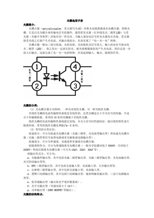
光耦选型手册光耦简介:光耦合器(opticalcoupler ,英文缩写为OC )亦称光电隔离器或光电耦合器,简称光耦。
它是以光为媒介来传输电信号的器件,通常把发光器(红外线发光二极管LED )与受光器(光敏半导体管)封装在同一管壳内。
当输入端加电信号时发光器发出光线,受光器接受光线之后就产生光电流,从输出端流出,从而实现了“电—光—电”转换。
光耦合器一般由三部分组成:光的发射、光的接收及信号放大。
输入的电信号驱动发光二极管(LED ),使之发出一定波长的光,被光探测器接收而产生光电流,再经过进一步放大后输出。
这就完成了电—光—电的转换,从而起到输入、输出、隔离的作用。
光耦的分类:(1)光电耦合器分为两种:一种为非线性光耦,另一种为线性光耦。
非线性光耦的电流传输特性曲线是非线性的,这类光耦适合于开关信号的传输,不适合于传输模拟量。
常用的4N 系列光耦属于非线性光耦。
线性光耦的电流传输特性曲线接近直线,并且小信号时性能较好,能以线性特性进行隔离控制。
常用的线性光耦是PC817A—C 系列。
(2)常用的分类还有:按速度分,可分为低速光电耦合器(光敏三极管、光电池等输出型)和高速光电耦合器(光敏二极管带信号处理电路或者光敏集成电路输出型)。
按通道分,可分为单通道,双通道和多通道光电耦合器。
按隔离特性分,可分为普通隔离光电耦合器(一般光学胶灌封低于5000V ,空封低于2000V )和高压隔离光电耦合器(可分为10kV ,20kV ,30kV 等)。
按输出形式分,可分为:a 、光敏器件输出型,其中包括光敏二极管输出型,光敏三极管输出型,光电池输出型,光可控硅输出型等。
b 、NPN 三极管输出型,其中包括交流输入型,直流输入型,互补输出型等。
c 、达林顿三极管输出型,其中包括交流输入型,直流输入型。
d 、逻辑门电路输出型,其中包括门电路输出型,施密特触发输出型,三态门电路输出型等。
e 、低导通输出型(输出低电平毫伏数量级)。
奥伦德 4通道的光耦
【原创实用版】
目录
1.光耦的概述
2.奥伦德 4 通道光耦的主要参数
3.奥伦德 4 通道光耦的应用场景
4.市场价格行情
正文
一、光耦的概述
光耦,全称光电耦合器,是一种电子元器件,具有光电转换功能。
它由发光元件(如 LED)和光敏元件(如光敏电阻)组成,两者之间通过光学耦合实现电信号与光信号的转换。
光耦具有输入和输出隔离、抗干扰能力强、传输信号质量高等优点,广泛应用于各种电子设备中。
二、奥伦德 4 通道光耦的主要参数
奥伦德 4 通道光耦(型号:PS2801)是一种具有 4 个通道的光电耦合器。
其主要参数如下:
1.输入类型:DC(直流)
2.输出类型:Transistor(晶体管)
3.隔离电压:该参数未在提供的参考信息中给出,需要进一步查询资料
三、奥伦德 4 通道光耦的应用场景
奥伦德 4 通道光耦可以应用于各种需要光电耦合的场景,如家电控制、工业自动化、通信设备等。
由于其具有 4 个通道,可以同时处理多个信号输入,提高设备的控制效率。
四、市场价格行情
根据提供的参考信息,2011 年奥伦德 4 通道光耦(型号:PS2801)的价格行情指数型号标识为 nec2801-4。
ucc2801工作原理ucc2801是一种常用的单片机外围设备,它可以用于控制和驱动各种类型的LED灯。
ucc2801的工作原理主要涉及到其内部的PWM调光控制电路和驱动电路。
ucc2801采用了PWM(脉宽调制)技术来控制LED灯的亮度。
PWM技术是一种通过改变信号的脉冲宽度来实现对电平平均值的控制方法。
ucc2801通过不断调整PWM信号的脉冲宽度,从而改变LED灯的亮度。
ucc2801内部的PWM调光控制电路主要由一个计数器和一个比较器组成。
计数器负责产生一个周期为T的脉冲信号,而比较器负责将计数器的输出信号与一个可调节的电压进行比较。
当计数器的输出信号大于可调节电压时,比较器输出高电平,反之输出低电平。
这样,通过调节可调节电压,可以控制PWM信号的脉冲宽度。
ucc2801的PWM调光控制电路还具有一个重要的特点,即可以通过外部引脚进行调光控制。
通过引脚的电平状态,可以选择是使用内部的可调节电压来控制PWM信号的脉冲宽度,还是使用外部的电压信号来控制PWM信号的脉冲宽度。
这样,用户可以根据实际需求选择合适的调光方式。
除了PWM调光控制电路,ucc2801还具有一个驱动电路,用于将PWM 信号转换为适合驱动LED灯的电压和电流。
驱动电路主要由电流源和开关管组成。
当PWM信号为高电平时,开关管导通,电流源将电流输入到LED灯中;当PWM信号为低电平时,开关管关断,电流源停止输出电流。
通过不断调节PWM信号的脉冲宽度,可以实现对LED灯亮度的精确控制。
总的来说,ucc2801通过PWM调光控制电路和驱动电路实现对LED 灯亮度的控制。
通过调节PWM信号的脉冲宽度,可以改变LED灯的亮度。
而通过驱动电路,可以将PWM信号转换为适合驱动LED灯的电压和电流。
这种工作原理使得ucc2801成为一种非常方便和高效的LED驱动器,广泛应用于照明和显示等领域。
在实际应用中,我们可以根据需要选择合适的ucc2801型号,并根据具体的LED灯参数进行配置。
NEC's 1 Mbps HIGH CMR ANALOG OUTPUT TYPE 8-PIN SOP HIGH-SPEED PHOTOCOUPLERFEATURES• HIGH ISOLATION VOLTAGE BV: 2500 V r.m.s.• HIGH COMMON MODE TRANSIENT IMMUNITY C MH , C ML = ±10 kV/ µs MIN • HIGH SUPPLY VOLTAGEV CC = 35 V• HIGH-SPEED RESPONSE t PHL = 0.8 µs MAX, t PLH = 1.2 µs MAXDESCRIPTIONNEC's PS8802-1 and PS8802-2 is an optically coupled isolator con t ain i ng a GaAIAs LED on the light emitting side (input side) and a PIN photodiode and a high-speed amplifer transistor on the output side on one chip.This is a plastic S08 type for high density applications.PS8802-1 PS8802-2ELECTRICAL CHARACTERISTICS (T A = 25°C)APPLICATIONS• COMPUTERS AND PERIPHERALS • GENERAL PURPOSE INVERTER• SUBSTITUTIONS FOR RELAYS AND PULSETRANSFORMERS • POWER SUPPLY • FACTORY AUTOMATION • SERIAL BUS ISOLATIONCalifornia Eastern LaboratoriesPRELIMINARY DATA SHEETPART NUMBERPS8802-1, PS8802-2D i o d eSYMBOLSPARAMETERSUNITS MINTYP MAX V FForward Voltage, I F = 16 mA V 1.72.2I R Reverse Current, V R = 3 VµA 10∆V F /∆T Forward Voltage Temperature Coef fi cient, I F = 16 mA mV/ºC -2.1C t Terminal Capacitance, V = 0, f = 1 MHzpF 30D e t e c t o rI OH (1)High Level Output Current, I F = 0 mA, V CC = V O = 5.5 V nA 3500I OH (2)High Level Output Current, I F = 0 mA, V CC = V O = 30 V µA 100V OL Low Level Output Voltage, I F = 16 mA, V CC = 4.5 V, I O = 1.2 mA V 0.10.4I CCL Low Level Supply Current, I F = 16 mA, V O = open, V CC = 30 V µA50I CCH High Level Supply Current, I F = 0 mA, V O = open, V CC = 30 V 0.012C o u p l e dCTR Current Transfer Ratio (IC/IF), I F = 16 mA, V CC = 30 V, V O = 0.4 V %152035R I-O Isolation Resistance, V I-O = 1 kV DC , RH = 40 to 60 %Ω1011C I-O Isolation Capacitance, C I-O = V = 0, f = 1 MHz pF 0.4t PHLPropagation Delay Time (H →L)1,I F = 16 mA, V CC = 30 V, R L = 2.2 k Ω, C L = 15 pF µs0.50.8t PLH Propagation Delay Time (L →H)1,I F = 16 mA, V CC = 30 V, R L = 2.2 k Ω, C L = 15 pF0.61.2C MH Common Mode Transient Immunity at High Level Output,I F = 0 mA, V CC = 5 V, R L = 2.2 k Ω, V CM = 1.5 kVkV/µs10C MLCommon Mode Transient Immunity at Low Level Output,I F = 16 mA, V CC = 5 V, R L = 4.1 k Ω, V CM = 1.5 kV-10(See notes on next page)元器件交易网PS8802-1, PS8802-2Notes:1.Operation in excess of any one of theseparameters may result in permanent damage. 2.Reduced to 1.00 mw/ºC at TA = 25ºC or more.3.AC voltage for 1 minute at T A = 25 ºC, RH = 60 % between input and ouput.ABSOLUTE MAXIMUM RATINGS 1 (T A = 25°C)SYMBOLS PARAMETERSUNITS RATINGS PS8802-1,-2DiodeI F Forward Current (DC)mA 25V R Reverse Voltage V 5.0P D Power Dissipation mW 45DetectorV CC Supply Voltage V 35V O Output Voltage V 35I O Output Current mA 8.0P C Power DissipationmW 100CoupledBV Isolation Voltage 2V r.m.s.2500T STG Storage Temperature°C -55 to +150T AOperating Ambient Temperature°C-55 to +100Notes:1.Test circuit for propagation delay time2.Test circuit for common mode transient immunity.PS8802-1(PW = 1µs,Duty cycle = 1/10)o (Monitor)L = 2.2k ΩPS8802-1VV OV OV OH (I F (I F 2 V 1 kV0 VOL PS8802-2CC = 5 V V o (Monitor)R L = 4.1k Ω元器件交易网OUTLINE DIMENSIONS(Units in mm)A Business Partner of NEC Compound Semiconductor Devices, Ltd.10/13/2003Life Support ApplicationsThese NEC products are not intended for use in life support devices, appliances, or systems where the malfunction of these products can reasonably be expected to result in personal injury. The customers of CEL using or selling these products for use in such applications do so at their own risk and agree to fully indemnify CEL for all damages resulting from such improper use or sale.PS8802-1, PS8802-2元器件交易网。
DATA SHEETThe information in this document is subject to change without notice. Document No. P12277EJ6V0DS00 (6th edition)Date Published May 1998 NS CP(K) Printed in Japan©1991 The mark • shows major revised points.DESCRIPTIONThe PS2801-1 and PS2801-4 are optically coupled isolators containing a GaAs light emitting diode and an NPN silicon phototransistor in a plastic SOP for high density applications.This package has shield effect to cut off ambient light.FEATURES•High isolation voltage (BV = 2 500 Vr.m.s.)•Small and thin package (4,16-pin SOP, Pin pitch 1.27 mm)•High collector to emitter voltage (V CEO = 80 V)•High-speed switching (t r = 3 µs TYP., t f = 5 µs TYP.)•UL approved: File No. E72422 (S)•VDE0884 approved (Option): PS2801-4 only•Operating number of taping product: PS2801-1-F3, F4, PS2801-4-F3, F4APPLICATIONS•Programmable logic controllers•Measuring instruments•Power supply•Hybrid ICPACKAGE DIMENSIONS (in millimeters)MARKING2ABSOLUTE MAXIMUM RATINGS (T A = 25 °C, unless otherwise specified)Parameter Symbol Ratings UnitPS2801-1PS2801-4Diode Forward Current (DC)I F50mAReverse Voltage V R6VPower Dissipation Derating∆P D/°C0.60.8mW/°CPower Dissipation P D6080mW/chPeak Forward Current*1I FP1ATransistor Collector to Emitter Voltage V CEO80VEmitter to Collector Voltage V ECO6VCollector Current I C50mA/chPower Dissipation Derating∆P C/°C 1.2mW/°CPower Dissipation P C120mW/chIsolation Voltage*2BV 2 500Vr.m.s.Operating Ambient Temperature T A−55 to +100°CStorage Temperature T stg−55 to +150°C*1PW = 100 µs, Duty Cycle = 1 %*2AC voltage for 1 minute at T A = 25 °C, RH = 60 % between input and output3ELECTRICAL CHARACTERISTICS (T A = 25 °C)Parameter Symbol Conditions MIN.TYP.MAX.UnitDiode Forward Voltage V F I F = 5 mA1.1 1.4VReverse Current I R V R = 5 V5µATerminal Capacitance C t V = 0 V, f = 1.0 MHz30pF Transistor Collector to EmitterDark CurrentI CEO V CE = 80 V, I F = 0 mA100nACoupled Current Transfer Ratio(I C/I F)CTR I F = 5 mA, V CE = 5 V80600%Collector SaturationVoltageV CE(sat)I F = 10 mA, I C = 2 mA0.3V Isolation Resistance R I-O V I-O = 1.0 kV DC1011ΩIsolation Capacitance C I-O V = 0 V, f = 1.0 MHz0.4pFRise Time*1t r V CC = 5 V, I C = 2 mA, R L = 100 Ω3µsFall Time*1t f5 *1Test circuit for switching timeV CC45TYPICAL CHARACTERISTICS (T A = 25 °C, unless otherwise specified)Ambient Temperature T A (˚C)D i o d e P o w e r D i s s i p a t i o n P D (m W )DIODE POWER DISSIPATION vs.AMBIENT TEMPERATUREAmbient Temperature T A ( ˚C)T r a ns i s t o r P o w e r D i s s i p a t i o n P C (m W )TRANSISTOR POWER DISSIPATION vs. AMBIENT TEMPERATUREForward Voltage V F (V)F o r w a r d C u r r e n t I F (m A )FORWARD CURRENT vs.FORWARD VOLTAGECollector to Emitter Voltage V CE (V)C o l l e c t o r C u r r e n t I C (m A )COLLECTOR CURRENT vs.COLLECTOR TO EMITTER VOLTAGEAmbient Temperature T A (˚C)C o l l e c t o r t o E m i t t er D a r k C u r r e n t I C E O (n A )COLLECTOR TO EMITTER DARKCURRENT vs. AMBIENT TEMPERATURECollector Saturation Voltage V CE(sat) (V)C o l l e c t o r C u r r e n t I C (m A )COLLECTOR CURRENT vs.COLLECTOR SATURATION VOLTAGE6FREQUENCY RESPONSEFrequency f (kHz)NormalizedGainGvLONG TERM CTR DEGRADATIONTime (Hr)CTR(RelativeValue)V CE = 5 V,n = 30.021000.1 1.01010020050150250300Forward Current I F (mA)CurrentTransferRatioCTR(%)CURRENT TRANSFER RATIO vs.FORWARD CURRENTNormalized to 1.0at T A = 25 ˚C,I F = 5 mA, V CE = 5 V,,,,,,,,,,,,,,,,,,,,,,,,,,,,,,,,,,,,,,,,,,,,,,,,,,,,,,,,,,,,,,,,,,,,,,,,,,,–500100–252550750.00.61.20.20.41.00.8Ambient Temperature T A (˚C)NormalizedCurrentTransferRatioCTRNORMALIZED CURRENT TRANSFERRATIO vs. AMBIENT TEMPERATURESwitchingTimet(s)µLoad Resistance R L (kΩ)SWITCHING TIME vs.LOAD RESISTANCELoad Resistance R L (kΩ)SWITCHING TIME vs.LOAD RESISTANCESwitchingTimet(s)µRemark The graphs indicate nominal characteristics.TAPING SPECIFICATIONS (in millimeters)PS2801-17PS2801-489RECOMMENDED SOLDERING CONDITIONS(1) Infrared reflow soldering •Peak reflow temperature235 °C (package surface temperature)•Time of temperature higher than 210 °C 30 seconds or less •Number of reflows Three•FluxRosin flux containing small amount of chlorine (The flux with a maximum chlorine content of 0.2 Wt % is recommended.)P a c k ag e S u r f a c e T e m p e r a t u r e T (˚C )Time (s)Recommended Temperature Profile of Infrared ReflowCaution Avoid removing the residual flux with chlorine-based cleaning solvent after a reflow process.(2) Dip soldering •Temperature 260 °C or below (molten solder temperature)•Time10 seconds or less •Number of times One•FluxRosin flux containing small amount of chlorine (The flux with a maximum chlorine content of 0.2 Wt % is recommended.)PROGRAMMABLE LOGIC CONTROLLERS EXAMPLE Purpose: In-out interface10[MEMO]11CAUTIONWithin this device there exists GaAs (Gallium Arsenide) material which is aharmful substance if ingested. Please do not under any circumstances break thehermetic seal.NEPOC is a trademark of NEC Corporation.No part of this document may be copied or reproduced in any form or by any means without the prior written consent of NEC Corporation. NEC Corporation assumes no responsibility for any errors which may appear in this document.NEC Corporation does not assume any liability for infringement of patents, copyrights or other intellectual property rights of third parties by or arising from use of a device described herein or any other liability arising from use of such device. No license, either express, implied or otherwise, is granted under any patents, copyrights or other intellectual property rights of NEC Corporation or others.While NEC Corporation has been making continuous effort to enhance the reliability of its semiconductor devices, the possibility of defects cannot be eliminated entirely. To minimize risks of damage or injury to persons or property arising from a defect in an NEC semiconductor device, customers must incorporate sufficient safety measures in its design, such as redundancy, fire-containment, and anti-failure features.NEC devices are classified into the following three quality grades:"Standard", "Special", and "Specific". The Specific quality grade applies only to devices developed based on a customer designated "quality assurance program" for a specific application. The recommended applications of a device depend on its quality grade, as indicated below. Customers must check the quality grade of each device before using it in a particular application.Standard: Computers, office equipment, communications equipment, test and measurement equipment, audio and visual equipment, home electronic appliances, machine tools, personal electronicequipment and industrial robotsSpecial: Transportation equipment (automobiles, trains, ships, etc.), traffic control systems, anti-disaster systems, anti-crime systems, safety equipment and medical equipment (not specifically designedfor life support)Specific: Aircrafts, aerospace equipment, submersible repeaters, nuclear reactor control systems, life support systems or medical equipment for life support, etc.The quality grade of NEC devices is "Standard" unless otherwise specified in NEC's Data Sheets or Data Books. If customers intend to use NEC devices for applications other than those specified for Standard quality grade, they should contact an NEC sales representative in advance.Anti-radioactive design is not implemented in this product.M4 96. 5。