PC400光耦资料
- 格式:pdf
- 大小:30.96 KB
- 文档页数:4


市场常见光耦内部图:光电耦合器(简称光耦)是开关电源电路中常用的器件。
光电耦合器分为两种:一种为非线性光耦,另一种为线性光耦。
常用的4N系列光耦属于非线性光耦常用的线性光耦是PC817A—C系列。
非线性光耦的电流传输特性曲线是非线性的,这类光耦适合于弄开关信号的传输,不适合于传输模拟量。
线性光耦的电流传输手特性曲线接进直线,并且小信号时性能较好,能以线性特性进行隔离控制。
开关电源中常用的光耦是线性光耦。
如果使用非线性光耦,有可能使振荡波形变坏,严重时出现寄生振荡,使数千赫的振荡频率被数十到数百赫的低频振荡依次为号调制。
由此产生的后果是对彩电,彩显,VCD,DCD等等,将在图像画面上产生干扰。
同时电源带负载能力下降。
在彩电,显示器等开关电源维修中如果光耦损坏,一定要用线性光耦代换。
常用的4脚线性光耦有PC817A----C。
PC111 TLP521等常用的六脚线性光耦有:TLP632 TLP532 PC614 PC714 PS2031等。
常用的4N25 4N26 4N35 4N36是不适合用于开关电源中的,因为这4种光耦均属于非线性光耦。
以下是目前市场上常见的高速光藕型号:100K bit/S:6N138、6N139、PS87031M bit/S:6N135、6N136、CNW135、CNW136、PS8601、PS8602、PS8701、PS9613、PS9713、CNW4502、HCPL-2503、HCPL-4502、HCPL-2530(双路)、HCPL-2531(双路)10M bit/S:6N137、PS9614、PS9714、PS9611、PS9715、HCPL-2601、HCPL-2611、HCPL-2630(双路)、HCPL-2631(双路)光耦合器的增益被称为晶体管输出器件的电流传输比 (CTR),其定义是光电晶体管集电极电流与LED正向电流的比率(ICE/IF)。
光电晶体管集电极电流与VCE有关,即集电极和发射极之间的电压。
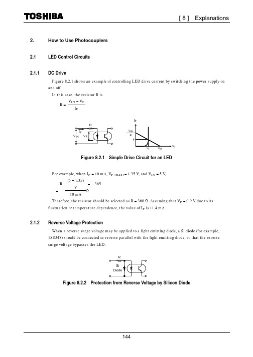
[8]Explanations2.How to Use Photocouplers2.1LED Control Circuits2.1.1DC DriveFigure 8.2.1 shows an example of controlling LED drive current by switching the power supply on and off. In this case, the resistor R is R= VIN − VF IFIF R IF VIN VFVIN R IF VFVFVINFigure 8.2.1 Simple Drive Circuit for an LEDFor example, when IF = 10 mA, VF (max) = 1.35 V, and VIN = 5 V, R = (5 − 1.35) V 10 mA = Ω 365Therefore, the resistor should be selected as R = 360 Ω. Assuming that VF = 0.9 V due to its fluctuation or temperature dependence, the value of IF is 11.4 mA.2.1.2Reverse Voltage ProtectionWhen a reverse surge voltage may be applied to a light emitting diode, a Si diode (for example, 1SS348) should be connected in reverse parallel with the light emitting diode, so that the reverse surge voltage bypasses the LED.R Si DiodeFigure 8.2.2 Protection from Reverse Voltage by Silicon Diode144[8]2.1.3 Threshold VoltageExplanationsWhen the input voltage is not absolutely zero or some unnecessary steady current flow is in a data transmission line, the threshold voltage of the LED should be raised up to a certain level by connecting a resistor in parallel with the light-emitting diode. (Figure 8.2.3)R VIN RSFigure 8.2.3 Threshold VoltageIf the forward voltage of the LED in the zero-light-emission state VT, the OFF-level input voltage VIN (OFF), and the OFF-level input current IIN (OFF) are given by VIN (OFF) = VT + R = (1 + IIN (OFF) = VT RS R RS VT RS ) VTThen in the case of the Toshiba IRED, the value of VT is 0.5 V.2.1.4Driving by Transistor or ICIn Figure 8.2.4 are shown examples of using an LED for driving circuits by utilizing a transistor or IC.VCC IF R IF VCCRR=VCC − VF − VCE (sat) IFR=VCC − VF − VOL IFFigure 8.2.4 Driving by Transistor or IC145[8]Explanations2.4Interface Circuit between TTLs Using a Phototransistor CouplerA circuit using a DIP 4 pin photocoupler as an interface between TTLs is shown in Figure 8.2.22. In order to assure positive ON/OFF operation of the TTL, the LED current IF should be set to satisfy IOL which is determined by RC and IIL. Example of Design Specifications Operating temperature: 0 to 70°C Data transmission rate: 5 kbit/s Supply voltage: VCC = 5 V ± 5% Operating life: 20 years (170,000 hours) System working ratio: 50% Specifications of products required for designing interface circuits are shown in Table 8.2.1.R IF VCC TLP521-1 VCC II IC RC IIL IC > II + IILFigure 8.2.22Interface Circuit between TTLs Using a 4 pin PhotocouplerTable 8.2.1 Principal Characteristics of the TLP521-1Item Forward voltage Collector to emitter Breakdown voltage Emitter to collector Breakdown voltage Collector dark current V (BR) ECO V (BR) CEO Symbol VF Test Condition (Ta = 25°C) IF = 10 mA IC = 0.5 mA IE = 0.1 mA IF = 0, VCE = 24 V IF = 0, VCE = 24 V, Ta = 85°C A rank Current transfer ratio CTR (IC/IF) IF = 5 mA VCE = 5 V GB rank GR rank BL rank Collector to emitter Saturation voltage VCE (sat) IF = 5 mA, IC = 1 mA min 1.0 55 typ. 1.15 ⎯ max 1.3 ⎯ Unit V V7 ⎯ ⎯ 50 100 100 200 ⎯⎯ 10 2 ⎯ ⎯ ⎯ ⎯ 0.1⎯ 100 50 600 600V nA µAICEO% 300 600 0.4 V146 155[8]2.4.1 Setting of RC (max)ExplanationsRC (max) should be set according to the switching time and dark current ICEO (max) at the maximum operating temperature of the photocoupler. The relations of switching time to RL (load resistance) and RC are shown as follows: As the data transmission rate is 5 kbit/s, the total switching time is T = tr + td + tf + ts < 200 µs = The load resistance RL is obtained from the switching time characteristic (for saturated operation) in Figure 8.2.23 so that T becomes 100 µs, taking account of variability in the device’s switching characteristic in order to secure T < 200 µs. RL < 4.7 kΩ is obtained from this graph. Here, RL can be = = expressed in terms of RC and the parallel resistance of the standard TTL input resistance RIN. (Figure 8.2.24) RL = RC ∥ RIN As RL = 4.7 kΩ > RIN = 4 kΩ, RC may be indefinite (RC = ∞) but RC (max) against the dark current ICEO (max) is limited. The relation between ICEO (max) and RC (max) is shown below. RC (max) = VCC (min) − VIH ICEO (max) + IIHThen, ICEO (max) must be estimated at Ta = 70°C. Temperature dependencies of ICEO (typ.) at alternative parameter values of VCE = 5 V, 10 V, and 24 V are shown in Figure 8.2.25.1000 800 600 400 200tf IF = 5 mA RL VOUTSwitching time (µs)100 80 60 40 20 10 8 6 4tsVOUT 5V 0V td tr tr90% 10% ts tf2 td 1 0 1 2 4 6 8 10 20 40 60 80 100Load resistance (kΩ)Figure 8.2.23 Load Resistance vs. Switching Time+5 V 4 kΩ TTL Coupler RINVCC RCFigure 8.2.24 RL can be Expressed by RIN and RC147 156[8]ExplanationsIn the case of the TLP521-1 phototransistor coupler, ICEO (max) = 50 µA at Ta = 85°C and VCE = 24 V. Therefore, taking VCE dependency and Ta dependency into consideration from Figure 8.2.25, ICEO(max) is estimated at Ta = 70°C and VE = 5 V.VCE dependency: ICEO (typ.) is reduced by 1/4 when VCE is varied form 24 to 5 V Ta dependency: ICEO (typ.) is reduced by 1/4 when Ta is varied form 85 to 70°C Therefore, ICEO (max) at Ta = 70°C and VCE = 5 V is estimated to be, ICEO (max) = 50 µA × 1 4 × 1 4 = 3.1 µAAccordingly, IIH is 40 µA for general TTLs and RC (max) will be obtained as follows: RC (max) = 4.75 V − 2 V 3.1 µA + 40 µA = 64 kΩ10 VCE = 24 V 110 5(µA) ICEO10−110−210−310−4 0 20 40 60 80 100 120Temperature (°C)Figure 8.2.25 ICEO vs. Temperature148 157[8]2.4.2 Setting of Forward Current IFExplanationsThe maximum forward current IF is obtained as IF = 16 mA subject to the constraint IF < IOL, and = the maximum allowable value of IF found from Figure 8.2.26 is 50 mA. However, IF should be kept as small as possible because CTR degradation increases with the increase of forward current. Figure 8.2.27 shows degradation of CTR. In order to realize the designed continuous operating life of approx imately. 100,000 hours, the forward current should be set at IF = 10 mA ± 50%.100 Test conditions IF = 70 mA, PC = 150 mW, Ta = 25°C80IC (t)/IC (t = 0) (VCE = 5 V, IF = 5 mA, Ta = 25°C)Allowable forward current(mA)1.0600.8400.6200.40 −200204060801000102103104Ambient temperature (°C)Test time (h)Figure 8.2.26 Ambient Temperature vs. Allowable Forward Current (TLP521-1)Figure 8.2.27Lifetime Test Data (CTR degradation)Setting of the IF limiting resistance RD Forward current (typ.) is expressed by the following formula: IF (typ.) = VCC − VF (typ) − VOL RD (typ)40 Ta = 25°C VCE = 5 Vwhere VF (typ.) is obtained from technical data. then, VF (typ.) = 1.15 V (at IF = 10 mA)(mA)20 10 6 4 2 IC/IF = 600% 370% 280% 185% 125% 80%Therefore, RD is determined as follows: RD = 5 V − 1.15 V − 0.4 V 10 mACollector current IC1 0.6 0.4 0.2= 345 Ω Therefore, RD = 330 Ω ± 5% will be optimum.0.1 0.06 0.04 0.4 6 8 1 2 4 6 10 20 40Forward current IF(mA)Figure 8.2.28IC vs. IF Curves Varying According to Different IC/IF Rations149 158[8]ExplanationsThen IF (min) and IF (max) should be checked to make sure that realized values of IF will remain within allowable tolerances: IF (min) = = VCC (min) − VF (max) − VOL RD (max) 4.75 V − 1.3 V − 0.4 V 314 Ω= 9.7 mA IF (max) = = VCC (max) − VF (min) − VOL RD (min) 5.25 V − 1.0 V − 0.4 V 347= 11.1 mA1.4 1.2 IF = 5 mARelative collector current1.02 mA1.2 5V 1.0 2V VCE = 0.4 V0.8IF = 10 mAIC/IF0.6 5 mA 0.40.80.20 0.10.6 0.2 0.4 0.6 0.8 1 2 4 6 8 10−20020406080100VCE(V)Ta(°C)Figure 8.2.29 IC/IF vs. VCESetting of pull-up resistance RCFigure 8.2.30 Collector Current vs. TaWhen the realized value of the collector current IC is assumed in the worst case to be min IC, RC can be expressed by the following relation: RC < = VCC (max) − VOLmin IC − IILmin IC = IC (min) × DIF × Dt × DVCE × DTa where, Dt: IC degradation rate after a certain time has passed. DIF: IC change rate at an IF setting for your designing. DVCE: IC drop rate under VCE (sat) condition. DTa: IC fluctuation rate with changes in the operating temperature Topr. These values are obtained from technical data. In the case of the TLP521-1:150 159[8]From Figure 8.2.27, Dt = 0.5 (t = 17 × 104 h, 50% operating ratio) From Figure 8.2.28, DIF = 2.5 (at IF = 10 mA) From Figure 8.2.29, DVCE = 0.8 (at VCE = 0.4 V) From Figure 8.2.30, DTa = 0.75 (at Ta = 70°C)ExplanationsOn the other hand, as IC (min) = 2.5 mA (at IF = 5 mA × IC/IF (min) = 50%), and min IC = 2.5 mA × 2.5 × 0.5 × 0.8 × 0.75 = 1.8 mA However, if based on these data, the following inequality cannot be met: min IC − IIL > VCC (max) − VOL RC (min)Therefore, a photocoupler with a higher CTR should be selected. In the case of the TLP521-1 (GB), because IC (min) is guaranteed to be 5 mA, the min IC will become 3.6 mA. Accordingly, IIL is 1.6 mA for general TTLs and RC (min) can be obtained as follows: RC (min) = 5.24 − 0.4 3.6 − 1.6 ∼ 2.4 kΩ −In other words, RC can be set from 2.4 kΩ to 64 kΩ, but it is also necessary to consider the switching speed required by a system and the requirement for certainty of logical ON or OFF conditions. If the switching speed is considered to be relatively more important, RC should be set to be near to RC (min). On the other hand, if the certainty of ON and OFF operation is considered to be the most important criterion, a value close to RC (max) should be selected (the operating life of the device may be defined as the period during which there is certainty of the ON and OFF conditions being properly set.). In this case, since Dt is assumed to be 0.5 with a relatively high margin the switching speed should be considered to be more important. So, RC is obtained as 4.7 kΩ.151 160[8]Explanations2.7Photocoupler Circuit Design2.7.1Transistor Output PhotocouplersFigure 8.2.33 shows a basic transistor photocoupler interface circuit, where collector current IC flows on the output side as IRED current IF is applied on the input side. The following points are important to determine each value in circuit design work: (1) IF = 0 (OFF state) Only a leakage current ID flows at the output transistor in this state. In order to maintain the OFF state, the output voltage VOUT (OFF) should be higher than VH (the required high level voltage) as follows: VCC − ID × RL = VOUT (OFF) > VH here, VCC: Applied voltage (supply voltage)RL VOUT IF ICVCCFigure 8.2.33 Transistor photocoupler152 163[8]ExplanationsThe leakage current ID increases as the ambient temperature rises (see Figure 8.2.34 Id vs. Ta), so the ID value will have to be considered at the worst case, which is at the maximum of operating temperature. Accordingly, the value of RL should meet the following formula: RL < VCC − VH IDlogIDTaFigure 8.2.34 Id vs. Ta(2) IF = Iin (ON state) When the collector current IC (ON) flows on the output side of the photocoupler, output VOUT (ON) has to be less than VL (the required low level voltage) as follows: VCC − IC (ON) × RL = VOUT (ON) < VL Accordingly, RL > VCC − VL IC (ON)Generally when the RL value is large, the switching response time increases, so the RL value should be kept as small as possible. (3) Considerations concerning the input current Iin in the “ON” status Normally technical data sheets of photocouplers show the characteristic curves IC vs. IF, CTR vs. Ta, and CTR vs. t as shown in Figure 8.2.35, Figure 8.2.36, Figure 8.2.37. The photocoupler CTR test is performed at the specific point be done by the following procedure; i) Draw the extrapolated CTR min curve (Note2) in parallel with the typical curve. Note2: This curve is the expected CTR min line. The cross point specification value. Here CTR = IC/IF, IC min = CTR min × IF1 ii) Find IF2 from the cross points of IC = IC (ON) with the B characteristic curve. This IF2 point indicates the minimum input current at Ta = 25°C and operating time t = 0 hour. When considering the relationship between CTR and Ta (Figure 8.2.36), as well as CTR degradation (Figure 8.2.37), the minimum input current Iin has to conform to the following formula.; Iin > IF2 × 1 DTa × 1 Dt ×α shows the “CTR min” in Figure 8.2.35. This point is not always the same as the actual operating point, so some compensation work is required toHere, DTa: Rate of CTR fluctuation within the operating temperature range Dt: CTR degradation rate after “t” hours of operation α: System design margin153 164Figure 8.2.39 I FT vs. TaFigure 8.2.40 I FT vs. tNote3: R S and C S are snubber circuits and recommended to be 47 Ω and 0.033 µF, respectively.I2.7.3 Photovoltaic CouplersRecently, in PBX systems, power MOSFETs* are beginning to replace mechanical relays. Thesepower MOSFETs require a voltage output type photocoupler (photovoltaic coupler).As devices become smaller, photorelays which combining a photovoltaic coupler and a MOSFET in a single package are starting to be used. As far as design is concerned, photovoltaic couplers andphotorelays are handled the same. In obtaining the photovoltaic output voltage to drive the MOSFET, how to determine input current I F is an important consideration.Figure 8.2.41 Photovoltaic CouplerIn photovoltaic couplers, both output voltage V OC , and short current I SC (output current) increase as input current increases. (see, Figure 8.2.42, Figure 8.2.45).Input current I in (Note4) has to be determined so that the output voltage V OC becomes high enough to drive the power MOSFET gate.These V OC and I SC values will change as a function of the ambient temperature Ta and operating time “t” as shown in Figure 8.2.43, Figure 8.2.46, and Figure 8.2.44.Considering these factors, the input current I in has to conform to the following formula:Figure 8.2.44 V OC vs. tvs. I Fvs. TaFigure 8.2.47 I SC vs. t1 1I in >I F ×D Ta × D t× αHere, D Ta : The fluctuation rate of V OC and I SC within the operating temperature range D t : The degradation rate of V OC and I SC after “t” hours of operationα: System design marginNote4: Turn-on time of the power MOSFET depends on the charging time of the gate capacitance. Thelarger the short current I SC (output current) becomes, the shorter the turn-on time is. So a power MOSFET transistor should be used whose input capacitance is as small as possible.Note5: There are many patents relating to MOSFET drivers.**: Normally this external resistor (high value) has to be connected. (1 M Ω)IVV2.7.4 I C Output Photocouplers(1) High-speed transistor output:6N135, 6N136, 6N138, 6N139TLP112, TLP112A, TLP114A, TLP550, TLP559, TLP759, TLP2530, TLP2531Output current I O depends upon input LED current I F and changes according to the formulaI O= CTR × I F (see Figure 8.2.48). This point should be considered in design work.As a representative example, the fundamental design rules in a TTL/TTL interface, which usesthe TLP550, are shown in Figure 8.2.49.Figure 8.2.48 I O vs. I F Figure 8.2.49 TTL/TTL Interface (TLP550)V CC1− V F− V OL1I O (min) = I F× CTR (min) R IN=I FV CC2− V OLR L(min)=I O(min) ×α+ I ILα: System design margin(2) High speed I C output:6N137TLP115A, TLP250, TLP251, TLP557, TLP558, TLP2200, TLP2601, TLP2630, TLP2631In these types, output status is inverted at a certain threshold I FH (or I FL) of input LEDcurrent I F (Figure 8.2.50). Therefore the input LED current I F should be designed to exceed themaximum specified value of I FH (or I FL) as shown in Figure 8.2.51.Figure 8.2.50 V O vs. I F Figure 8.2.51 TTL/TTL Interface (TLP2601)V CC1− V F− V OL1R IN (max)=I FH (max) ×α(α: system design margin)I FVFlogITable 8.2.2 I FH , I FL max SpecificationsProduct Number I FH (or I FL ) maxGuaranteed temperature range6N137, TLP115ATLP2601, TLP2630 TLP2631 5 mA0 to 70°C TLP557−30 to 70°C TLP250, TLP251 5 mA −20 to 70°C TLP2200, TLP5581.6 mA−25 to 85°C(3) Other precautions(a) Bypass capacitorHigh-gain amplifiers are built into the output detector I C in the photo I C couplers. Due to noise voltage on the V CC power line or on the GND line, or because of the V CC transient voltage caused by load switching, internal oscillation may occur and lead to abnormal operation. To prevent this, a bypass capacitor (0.1 µF) with good high-frequencycharacteristics should be connected between V CC and GND within 1 cm from each pin. (see Figure 8.2.52)The 0.1 µF bypass capacitor should be connected for the following I C output couplers; 6N137, TLP113, TLP115, TLP115A, TLP558, TLP2601, TLP2630, TLP2631 Toshiba recommends 0.1 µF bypass capacitor to use externally to all IC output type photocouplers for designing safety.Figure 8.2.52 Bypass Capacitor (ceramic)(b) Enable terminalsThe 6N137, TLP2200, TLP2601 and TLP558 all have enable terminals. When not utilizing this enable function, the terminals are to be treated as follows;Figure 8.2.53 Enable Terminal Treatment(c) Photocoupler insulation performanceOur photocoupler insulation performance designations are based on maintaining that performance for a period of one minute. This equipment is not generally recommended for applications using high voltage for long continuous periods. If the usage may involve a long continuous period of exposure to high voltage, contact a Toshiba sales office.6N137 TLP2601CCV E (pin 7): Open (or V CC directly connected) 1324V E (pin 6): GND Directly Connected V E (pin 7): V CC Directly ConnectedCC。

光电耦合器p c中文资料 The Standardization Office was revised on the afternoon of December 13, 2020光电耦合器pc817中文资料PC817光电耦合器广泛用在电脑终端机,可控硅系统设备,测量仪器,影印机,自动售票,家用电器,如风扇,加热器等电路之间的信号传输,使之前端与负载完全隔离,目的在于增加安全性,减小电路干扰,减化电路设计。
特点:电流传输比(CTR: MIN. 50% at IF=5mA ,VCE=5V)高隔离电压:5000V有效值公认的UL认证,档案编号E64380* 2 40至60%相对湿度,交流1分钟* 3 10秒Response time 响应时间Rise time 上升时间tr VCE = 2V, I C =2mA, R L = 100 W- 4 18 μs Fall time下降时间tf - 3 18 μsModel No. 型号Rank mark 等级标志电流传输比CTR ( % )PC817A A 80 to 160PC817B B 130 to 260PC817C C 200 to 400PC817D D 300 to 600PC8 * 7AB A 或 B 80 to 260PC8 * 7BC B 或C 130 to 400PC8 * 7CD C 或 D 200 to 600PC8 * 7AC A, B 或 C 80 to 400PC8 * 7BD B, C 或 D 130 to 600PC8 * 7AD A, B, C 或 D 80 to 600PC8 * 7 A, B, C, D 或无标记50 to 600图1测试电路的频率响应图2测试电路的响应时间特性曲线图正向电流比(常温) 集电极功耗比(常温)峰值正向电流与占空比电流传输比比正向电流正向电流与正向电压集电极电流比集电极发射极电压相对比率与电流传输比常温集电极发射极饱和电压与常温集电极暗电流比常温响应时间与负载电阻频率响应集电极发射极饱和电压与正向电流应用电路:图4 打开或关闭12V直流电动机的TTL控制信号输入电路图图5 与TL431配合的电源反馈电路封装尺寸及功能图:译自sharp公司。
SEN02223-15-8-8-8-870001700017000170001e p c a t al o g s .c ome p c a t a l o g s .c o mPC400, 450-81SEN02225-15HYDRAULIC EXCAVATORPC400-8PC400LC-8PC450-8PC450LC-8Machine model Serial numberPC400-870001 and up PC400LC-870001 and up PC450-870001 and up PC450LC-870001 and up00 Index and forewordIndexComposition of shop manual ..........................................................................................................................2Table of contents (4)e pc at al o g s .c omSEN02225-1500 Index and foreword2PC400, 450-8Composition of shop manualThe contents of this shop manual are shown together with Form No. in a list.Note 1:Always keep the latest version of this manual in accordance with this list and utilize accordingly.The marks shown to the right of Form No. denote the following:Q : New issue (to be filed additionally)q : Revision (to be replaced for each Form No.)Note 2:This shop manual can be supplied for each Form No.Note 3:To file this shop manual in the special binder for management, handle it as follows:•Place a divider on the top of each section in the file after matching the Tub No. with No. indicated next to each Section Name shown in the table below:•File overview and other materials in sections in the order shown below and utilize them accord-ingly.Section TitleForm NumberShop Manual, contents binder, binder label and tabs SEN02223-1500 Index and foreword SEN02224-15IndexSEN02225-15q Foreword and general information SEN02226-0201 SpecificationSEN02227-02Specification and technical dataSEN02228-0210 Structure, function and maintenance standard SEN02229-08Engine and cooling system SEN02230-00Power trainSEN02231-00Undercarriage and frame SEN02232-00Hydraulic system, Part 1SEN02233-00Hydraulic system, Part 2SEN02234-04 Hydraulic system, Part 3SEN02235-02q Work equipmentSEN02236-00Cab and its attachments SEN02237-00Electrical system SEN02238-0320 Standard value tableSEN02239-03Standard service value table SEN02643-0330 Testing and adjustingSEN02240-07Testing and adjusting, Part 1SEN02644-04Testing and adjusting, Part 2SEN02645-06Testing and adjusting, Part 3SEN02662-0240 TroubleshootingSEN02241-04Failure code table and fuse locations SEN02646-03General information on troubleshootingSEN02647-03Troubleshooting by failure code (Display of code), Part 1SEN02648-04Troubleshooting by failure code (Display of code), Part 2SEN02649-03Troubleshooting by failure code (Display of code), Part 3SEN02650-04Troubleshooting of electrical system (E-mode)SEN02651-03Troubleshooting of hydraulic and mechanical system (H-mode)SEN02652-03e pc at al o g s .c om00 Index and foreword SEN02225-15PC400, 450-83Troubleshooting of engine (S-mode)SEN02653-0250 Disassembly and assemblySEN02242-07General information on disassembly and assembly SEN02654-03Engine and cooling system SEN02655-01Power trainSEN02656-02Undercarriage and frame SEN02657-04Hydraulic system SEN02658-01Work equipmentSEN02659-01q Cab and its attachments SEN02660-01Electrical system SEN02661-0290 Diagrams and drawingsSEN02243-04Hydraulic diagrams and drawings SEN02244-01q Electrical diagrams and drawingsSEN02245-03e pc at al o g s .c omBuy nowKomatsu Hydraulic Excavator PC400 -8, PC400LC-8, PC450 -8, PC450LC-8 Shop Manual PDFWith Instant Download。
PC400光耦资料s Featuress Outline DimensionsPC400PC400“In the absence of confirmation by device specification sheets, SHARP takes no responsibility for any defects that occur in equipment using any of SHARP's devices, shown incatalogs,Compact, Surface Mount Type OPIC Photocoupler (Unit :mm )查询PC400供应商020010015010050025*********Fig. 2 Power Dissipation vs. Ambient TemperatureAmbient temperature T a (?C )P o w e r d i s s i p a t i o n PO , P t o t (m W )1020605040300-25025*******85Fig. 1 Forward Current vs. Ambient TemperatureF (m A )Ambient temperature T a (?C )0.2R e l a t i v e t h r e s h o l d i n p u t c u r r e n t0.40.61.451020151.21.00.8Supply voltage V CC (V )1251020501002005000.51.0 1.52.0 2.53.0F (m A )Fig. 3 Forward Current vs. Forward VoltageForward voltage V F (V )Fig. 4 Relative Threshold Input Current vs. Supply Voltage0.20.4R e l a t i v e t h r e s h o l d i n p u t c u r r e n t0.60.81.62550100-25751.41.21.0Ambient temperature T a (?C )0.0110.020.050.11.0251010050200.20.5L o w l e v e l o u t p u t v o l t a g e V O L (V )Low level output current I OL (mA )Fig. 5 Relative Threshold Input Current vs. Ambient TemperatureFig. 6 Low Level Output Voltage vs. Low Level Output CurrentF o r w a r d c u r r e n t I F o r w a r d c u r r e n t I -25P tot P OIFHLIFLHT a =25?CI FHL =1 at V CC =5V IFHLIFLHV CC =5VI FHL =1 at T a =25?C V CC =5VI F =4mA T a =25?C0.20.30.5-0.100.4L o w l e v e l o u t p u t v o l t a g e V O L (V )Fig. 7 Low Level Output Voltage vs. Ambient TemperatureSupply Voltage012345(μs )L (k ?)Forward current I F (mA )P r o p a g a t i o n d e l a y t i m e Fig. 8 Supply Current vs.s Preautions for UseGND near the device in order to stabilize power supply line.(2) Handle this product the same as with other integrated circuits against static electricity.(3) As for other general cautions, refer to the chapter “Precautions for Use ”(1) It is recommended that a by-pass capacitor of more than 0.01μF be added between V CC and Load resistance R。
400VMCC和PC系统讲课内容
1,PC、MCC含义:
MCC:称为电动机(或马达)控制中心,〈75kW的电动机一般分布在400MCC 母线。
PC:称为低压动力中心,75kW~200kW和150~650kW静态负荷一般分布在400VPC母线。
2,全厂PC母线列表:
3,系统图:见附件
4,保安段的主要负荷:
BOP、顶轴油泵、EH油泵、汽机盘车、真空破坏阀、氢侧密封油泵;
扫描风机、空预器主变频器、引风机盘车、磨煤机液压油泵、空预器下轴承油泵、密封风机、空预器漏风控制柜保安电源、#1炉锅炉吹灰器动力电源、AH-05送风机;UPS的工作和旁路电源、充电器、400VPC1A7-1保安电源开关1A4-3P。
5,400VPC系统运行方式:
每一400V的PC单元设两段母线,每段母线通过一台低压厂用变压器供电,两台变压器的高压侧分别接至厂用高压母线的不同分段上。
两台低压母线之间设一联络开关,两台低压厂变互为暗备用。
一台厂变因故停役时,另一台厂变能满足两段母线负荷运行的要求。
a,按A、B系列分布的400VPC采用单母线分段运行方式,其联络开关正常处于冷备用状态。
b,400VPC1A7及1A7-1母线:1A7T合闸,由1A7L开关供电,,1A4-3p开关合闸,1A7-1N开关处于热备用状态,投入“自动”方式。
c,400VMCC12A4-3母线正常由PC1B4母线供电;400VMCC22A4-3正常由PC2B4母线供电。