DW02D(锂电池保护IC)
- 格式:pdf
- 大小:296.94 KB
- 文档页数:8
DW03一、描述DW03产品是单节锂离子/锂聚合物可充电电池组保护的高集成度解决方案。
DW03包括了先进的功率MOSFET,高精度的电压检测电路和延时电路。
DW03具有非常小的SOT23-5的封装,这使得该器件非常适合应用于空间限制得非常小的可充电电池组应用。
DW03具有过充,过放,过流,短路等所有的电池所需要保护功能,并且工作时功耗非常低。
该芯片不仅仅为手机而设计,也适用于一切需要锂离子或锂聚合物可充电电池长时间供电的各种信息产品的应用场合。
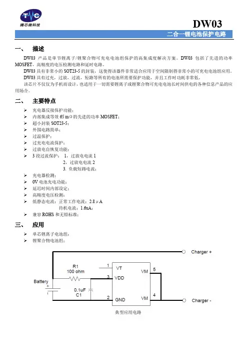
二、主要特点充电器反接保护功能;内部集成等效65 mΩ的先进的功率MOSFET;超小封装SOT23-5;外围电路简单;过温保护;过充电电流保护;过放电自恢复功能;3段过流保护:1,过放电电流12,过放电电流23. 负载短路电流;充电器检测;0V电池充电功能;延迟时间内部设定;高精度电压检测;低静态电流:正常工作电流:2.8μA待机电流:1.6uA;兼容ROHS和无铅标准;三、应用单芯锂离子电池组;锂聚合物电池组;典型应用电路四、 订货信息注意:“YW ”代表日期,“Y ”代表年份,“W ”代表星期五、 管脚外形及描述六、 极限参数DW03七、 电气特性参数(除非特别指定,AT=25℃)DW03功能框图VM八、 功能描述DW03监控电池的电压和电流,并通过断开充电器或负载,保护单节可充电锂电池不会因为过充电压,过放电压,过充电流,过放电流以及短路等情况而损坏。
系统外围电路简单。
MOSFET 已内置,等效电阻典型值为65m Ω。
正常工作模式如果没有检测到任何异常情况,输出管一直打开,充电和放电过程都将自由转换。
这种情况称为正常工作模式。
过充电压情况(OCV )在正常条件下的充电过程中,当电池电压高于过充检测电压(VCU ),并持续时间达到过充电压检测延迟时间(tCU )或更长,DW03将关断MOSFET 以停止充电。
这种情况称为过充电压情况。
以下两种情况下,过充电压情况将被释放:1、 当电池电压低于过充解除电压(VCL ),DW03打开输出管,回到正常工作模式。
精心整理DW01锂电池保护IC一、主要特性静态电流待机电流(检测到过放之后)过充检测精度(Topt=25℃)过充检测精度(Topt=0到50℃)过放检测精度过放检测电压过流保护过充延迟(VDD=4.4V)过放延迟(VDD=2.2V带有内置电容)封装典型值:4.0uA典型值:0.2uA±50mV±60mV±100mV2.0V到3.0V,每步0.005V 0.04V到0.32V,每步0.04V 110mS22mS(最小值)SOT23-6/6-pin二、基本描述DW01是一款单节可充电锂电池保护集成电路,具有过充、过放、过流及短路保护功能。
IC内部包含:三个电压检测电路、一个基准电路、一个延迟电路、一个短路保护电路和一个逻辑电路。
当充电电压逐渐增大超过过充检测电路的阈值VDET1时,Cout Pin的输出电压即过充检测电路的输出电压VD1会变到低电位,也就是充电器负端的电位。
在进入过充保护状态后,当VDD电压降低到VREL1下方或者当电池组脱离充电器而接一个负载,且VDD介于VDET1与VREL1之间时VD1可以复位,即CoutPin输出变为高电位。
当放电电压低于过放检测电路的阈值VDET2时,经过一段固定的延迟时间,Dout Pin的输出即过放检测电路的输出VD2会变为低电位。
这时,若给电池充电,当电池电压上升到过放检测电路的阈值电压之上时,VD2恢复,Dout的输出电压变为高电平。
当有过流情况出现时,内部过流检测电路会检测到,经过一段固定的延迟时间后,VD3和Dout变为低电平,放电回路被切断。
这时,若将电池组从负载系统中分开,VD3会恢复使Dout 变为高电平。
当有外部短路电流时,短路保护电路会立即使Dout变为低电位,当外部短路电流消失后,Dout会转换为高电位。
在检测到过放之后,会通过关闭一些内部电路使电源电流非常低。
IC过充检测电路的延迟时间可以通过连接外部电容进行设置。
一、 概述本文着重介绍单节锂电池保护IC 注:单颗IC ,而非保护板)的测试方法。
比较下,测试单颗保护IC 的优点是可以准确的测出IC 的电气特性,且因外部线路已固定,可以直接判断IC 的好坏;它的缺点则是测试速度较慢,另因IC 在上板前的抗静电能力较弱,故对测试人员和测试环境的ESD 防护要求也较高。
DW01D 是富满电子半导体股份有限公司所研发出的单节锂电池保护IC 之一,它具有过充保护、 过放保护和过二、1. (M22. (M13. 降)会通过和P-状 态下,L i t h i u m -I o n4.不正常充电电流的侦测功能:正常充电时,如果充电电流很大,CSI侦测到的电压(这个大的电流在两个导通的MOS管上所产生的压降)低于不正常充电侦测电压(VCH),它会通过OC pin 相对于CS的电平由高到低,转换控制充电的MOSFET(M2)管由导通到断开,切断充电回路。
1.正常工作时的耗电流(IDD)的测试方法测量示意图,见图2。
CSI短接到GND。
用FLUKE 5500A 模拟电池,从VCC输入3.9V(V1),使IC处于正常工作状态,闭合开关K,确认OC输出为高出为低电平。
CSI短接到GND。
V1由FLUKE 5500A 提供,FLUKE 5500A输出一个VPP 为 1.6V、OFFSET 为 2.8V、频率为10Hz的方波,OD 的电平也会变为一个有规律的波形。
用示波器比较V1和OD 的电平波形,可得到过放保护延迟时间TOD。
9.过流保护延迟时间(TOI1)的测试方法测量示意图,见图10。
V1由稳压电源提供,电压为3.6V,使IC处于正常工作状态。
V2由FLUKE 5500A 提供,FLUKE 5500A 输出一个VPP为0.3V、OFFSET 为 0.1V、频率为10Hz的方波,OD过电流2(短路电流)检测迟延时间TOI2 VDD=3.6V -- 5 50 us 其他OC管脚输出高电平电压V oh1 -- VDD-0.1 VDD-0.02 -- V OC管脚输出低电平电压V ol1 -- -- 0.01 0.1 V OD管脚输出高电平电压V oh2 -- VDD-0.1 VDD-0.02 -- V OD管脚输出低电平电压V ol2 -- -- 0.01 0.1六、波形图过流延时测试结果图:过充保护测试结果图:过充恢复测试结果图:过放保护测试结果图:过放恢复测试结果图:过充延时测试结果图:过放延时测试结果图:短路延时测试结果图:。
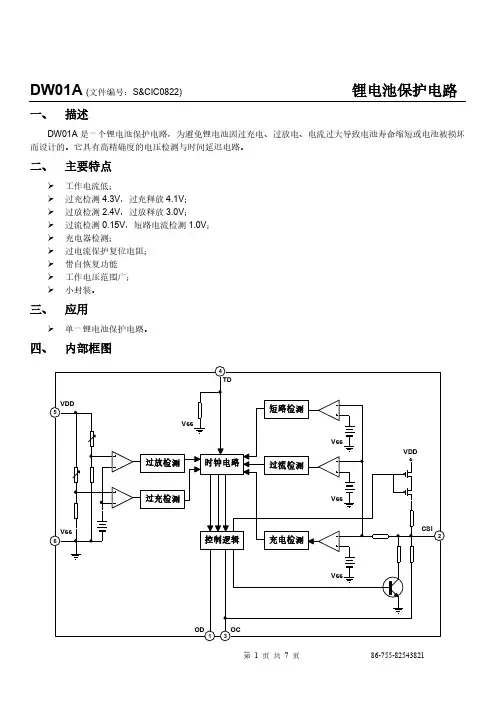
DW01A (文件编号:S&CIC0822)锂电池保护电路一、描述DW01A是一个锂电池保护电路,为避免锂电池因过充电、过放电、电流过大导致电池寿命缩短或电池被损坏而设计的。
它具有高精确度的电压检测与时间延迟电路。
二、主要特点工作电流低;过充检测4.3V,过充释放4.1V;过放检测2.4V,过放释放3.0V;过流检测0.15V,短路电流检测1.0V;充电器检测;过电流保护复位电阻;带自恢复功能工作电压范围广;小封装。
三、应用单一锂电池保护电路。
DW01A (文件编号:S&CIC0822)锂电池保护电路五、极限参数六、电气特性参数(除非特别指定,Tamb=25℃)过充电状态当从正常状态进入充电状态时,可以通过VDD检测到电池电压。
当电池电压进入到这充电状态时,VDD 电压大于VOC P,迟延时间超过TOC,M2关闭。
释放过充电状态进入过充电状态后,要解除过充电状态,进入正常状态,有两种方法。
●如果电池自我放电,并且VDD<VOCR,M2开启,返回到正常状态。
●在移去充电器,连接负载后,如果VDD<VOCP,M2开启,返回到正常模式。
过放电检测当由正常状态进入放电状态时,可以通过VDD检测到电池电压。
当电池电压进入过放电状态时,VDD电压小于VOD P,迟延时间超过TOD,则M1关闭。
释放过放电模式如果在过放电模式有一个充电器连接电池,电压将变为VCSI<VC HA和VDD>VODR,M1开启并返回到常模式;或者当负载悬空,VDD电压恢复到VDD>VODR,M1开启并返回到正常模式(自恢复功能)。
充电检测当一个充电器连接电池,电压将变为VCSI<VCHA,这样IC检测到充电器已接入。
过电流/短路电流检测在正常模式下,当放电电流太大时,由CSI管脚检测到电压大于VOIX(V OI1或V OI2),并且迟延大于TOIX(T OI1或T OI2),则代表过电流(短路)状态。
dw01原理图DW01原理图。
DW01原理图是指DW01电池保护IC的电路原理图,用于实现对锂电池的保护和管理。
DW01是一种专门设计用于锂离子电池保护的集成电路,它可以监测电池的电压、电流和温度,并在必要时切断电池的输出,以防止电池过充、过放、过流和过温,从而延长电池的使用寿命,并确保电池的安全性能。
DW01原理图主要包括DW01芯片、电池接口、电池连接线、保险丝、电源接口、电源管理芯片等几个主要部分。
通过这些部分的合理连接和布局,可以实现对锂电池的全面保护和管理。
首先,DW01芯片是整个电路的核心部分,它通过监测电池的电压、电流和温度,实时掌握电池的工作状态。
一旦发现电池处于过充、过放、过流或过温状态,DW01芯片会立即切断电池的输出,以保护电池不受损害。
其次,电池接口和电池连接线是用来连接锂电池和DW01芯片的重要部分,它们负责传输电池的电压和电流信息给DW01芯片,并接收DW01芯片的保护指令,以实现电池保护和管理的功能。
另外,保险丝是用来保护电路的重要部分,一旦电路中出现过流情况,保险丝会立即熔断,切断电路,保护电路不受损害。
此外,电源接口和电源管理芯片是用来为DW01芯片提供工作电压和管理电源的重要部分,它们负责为DW01芯片提供稳定的工作电压和电源管理功能,以确保DW01芯片能够正常工作。
综上所述,DW01原理图是一种用于锂电池保护和管理的电路原理图,通过合理连接和布局DW01芯片、电池接口、电池连接线、保险丝、电源接口和电源管理芯片等部分,可以实现对锂电池的全面保护和管理,延长电池的使用寿命,并确保电池的安全性能。
DW01原理图的设计和应用,对于锂电池的保护和管理具有重要的意义,可以广泛应用于各种类型的锂电池产品中。
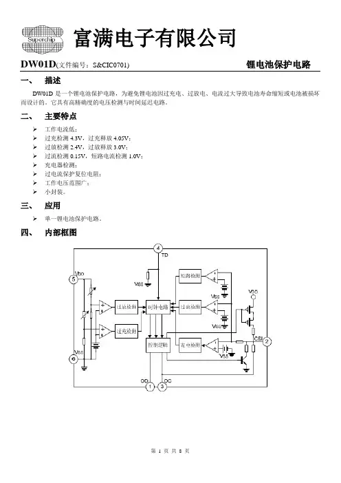
DW01D(文件编号:S&CIC0701) 锂电池保护电路一、描述DW01D是一个锂电池保护电路,为避免锂电池因过充电、过放电、电流过大导致电池寿命缩短或电池被损坏而设计的。
它具有高精确度的电压检测与时间延迟电路。
二、主要特点工作电流低;过充检测4.3V,过充释放4.05V;过放检测2.4V,过放释放3.0V;过流检测0.15V,短路电流检测1.0V;充电器检测;过电流保护复位电阻;工作电压范围广;小封装。
三、应用单一锂电池保护电路。
四、内部框图DW01D(文件编号:S&CIC0701) 锂电池保护电路五、极限参数六、电气特性参数(除非特别指定,Tamb=25℃)DW01D(文件编号:S&CIC0701) 锂电池保护电路七、管脚排列图八、功能描述正常条件如果VODL>VDD>VOCU,并且VCH<VCSI<VOI1,那么M1和M2都开启(见典型应用电路图)。
此时充电和放电均可以正常进行。
过充电状态当从正常状态进入充电状态时,可以通过VDD检测到电池电压。
当电池电压进入到这充电状态时,VDD 电压大于VOCU,迟延时间超过TOC,M2关闭。
释放过充电状态进入过记电状态后,要解除过记电状态,进入正常状态,有两种方法。
●如果电池自我放电,并且VDD<VOCR,M2开启,返回到正常状态。
●在移去充电器,连接负载后,如果VOCR<VDD<VOCU,VCSI>VOI1,M2开启,返回到正常模式。
过放电检测当由正常状态进入放电状态时,可以通过VDD检测到电池电压。
当电池电压进入过放电状态时,VDD电压小于VODL,迟延时间超过TOD,则M1关闭。
此时CSI管脚通过内部电阻RCSID拉到VDD。
如果VCSI>VOI2,则电路进入断电模式(电流小于0.3uA)。
释放断电模式当电池在断电模式时,若连接入一个充电器,并且此时VCH<VCSI<VOI2,VDD<VODR,M1仍旧关闭,但是释放断电模式。
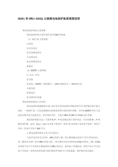
S8261和DW01-8205A主流锂电池保护板原理图说明锂电池保护板的主要参数锂电池保护板主要由保护IC和MOS管构成(1)保护IC主要参数1)封装2)过充电压3)过充释放电压4)过放电压5)过放释放电压6)耐压(2) MOSFET主要参数1) N沟、P沟2)内阻3)封装(TSSOP8 <简称薄片>、SOP8<简称厚片>、SOT23-6等)4)耐电流5)耐电压6)内部是否连通锂电池保护板的工作原理锂电池保护板根据使用IC,电压等不同而电路及参数有所不同,保护板有两个核心部件:一块保护IC,它是由精确的比较器来获得可靠的保护参数;另外是MOSFET串在主充放电回路中担当高速开关,执行保护动作。
下面以DW01配MOS管8205A进行讲解:激活保护板的方法:当保护板P+、P-没有输出处于保护状态,可以短路B-、P-来激活保护板,这时,Dout、Cout均会处于低电平(保护IC此两端口是高电平保护,低电平常态)状态打开两个MOS开关。
1.锂电池保护板其正常工作过程为:当电芯电压在至之间时,DW01的第1脚、第3脚均输出高电平(等于供电电压),第二脚电压为0V。
此时DW01的第1脚、第3脚电压将分别加到8205A的第5、4脚,8205A 内的两个电子开关因其G极接到来自DW01的电压,故均处于导通状态,即两个电子开关均处于开状态。
此时电芯的负极与保护板的P-端相当于直接连通,保护板有电压输出。
2.保护板过放电保护控制原理:当电芯通过外接的负载进行放电时,电芯的电压将慢慢降低,同时DW01内部将通过R1电阻实时监测电芯电压,当电芯电压下降到约时DW01将认为电芯电压已处于过放电电压状态,便立即断开第1脚的输出电压,使第1脚电压变为0V,8205A内的开关管因第5脚无电压而关闭。
此时电芯的B-与保护板的P-之间处于断开状态。
即电芯的放电回路被切断,电芯将停止放电。
保护板处于过放电状态并一直保持。
一、主要特性静态电流待机电流(检测到过放之后)过充检测精度(Topt=25℃)过充检测精度(Topt=0 到50℃)过放检测精度过放检测电压过流保护过充延迟(VDD=4.4V)过放延迟(VDD=2.2V 带有内置电容)封装典型值:4.0uA典型值:0.2uA±50mV±60mV±100mV2.0V 到3.0V,每步0.005V 0.04V 到0.32V,每步0.04V 110mS22mS(最小值)SOT23-6/6-pin二、基本描述DW01 是一款单节可充电锂电池保护集成电路,具有过充、过放、过流及短路保护功能。
IC 内部包含:三个电压检测电路、一个基准电路、一个延迟电路、一个短路保护电路和一个逻辑电路。
当充电电压逐渐增大超过过充检测电路的阈值VDET1 时,Cout Pin 的输出电压即过充检测电路的输出电压VD1 会变到低电位,也就是充电器负端的电位。
在进入过充保护状态后,当VDD 电压降低到VREL1 下方或者当电池组脱离充电器而接一个负载,且VDD 介于VDET1 与VREL1 之间时VD1 可以复位,即Cout Pin 输出变为高电位。
当放电电压低于过放检测电路的阈值VDET2 时,经过一段固定的延迟时间,Dout Pin 的输出即过放检测电路的输出VD2 会变为低电位。
这时,若给电池充电,当电池电压上升到过放检测电路的阈值电压之上时,VD2 恢复,Dout 的输出电压变为高电平。
当有过流情况出现时,内部过流检测电路会检测到,经过一段固定的延迟时间后,VD3 和Dout 变为低电平,放电回路被切断。
这时,若将电池组从负载系统中分开,VD3 会恢复使Dout 变为高电平。
当有外部短路电流时,短路保护电路会立即使Dout变为低电位,当外部短路电流消失后,Dout 会转换为高电位。
在检测到过放之后,会通过关闭一些内部电路使电源电流非常低。
IC 过充检测电路的延迟时间可以通过连接外部电容进行设置。
DW02S______________________________________ ________________________________________________________________ One Cell Lithium-ion/Polymer Battery Protection ICGENERAL DESCRIPTIONThe DW02S series product is a high integration solution for lithium-ion/polymer battery protection.DW02S contains advanced power MOSFET, high-accuracy voltage detection circuits and delay circuits. DW02S is put into an ultra-small SOT23-3 package and only oneexternal component makes it an ideal solution in limited space of battery pack. DW02S has all the protection functions required in the battery application including overcharging, overdischarging, overcurrent and load short circuiting protection etc. The accurate overcharging detection voltage ensures safe and full utilization charging. The low standby current drains little current from the cell while in storage.The device is not only targeted for digital cellular phones, but also for any other Li-Ion and Li-Poly battery-powered information appliances requiring long-term battery life.FEATURES· Protection of Charger Reverse Connection· Protection of Battery Cell Reverse Connection· Integrate Advanced Power MOSFET with Equivalent of 56m R SS(ON) · Ultra-small SOT23-3 Package · Only One External Capacitor Required· Over-temperature Protection · Overcharge Current Protection · Two-step Overcurrent Detection: -Overdischarge Current -Load Short Circuiting· Charger Detection Function · 0V Battery Charging Function- Delay Times are generated inside · High-accuracy Voltage Detection · Low Current Consumption- Operation Mode: 2.8μA typ. - Power-down Mode: 1.5μA typ. · RoHS Compliant and Lead (Pb) FreeAPPLICATIONSOne-Cell Lithium-ion Battery Pack Lithium-Polymer Battery PackFigure 1. Typical Application CircuitDW02S________ ____________________________________________________ ______ORDERING INFORMATIONPART NUMBER Pack age Overcharg e Detection Voltage [V CU ] (V) Overcharge ReleaseVoltage [V CL ] (V) Overdischarge Detection Voltage [V DL ] (V) Overdischarge Release Voltage [V DR ] (V) OvercurrentDetection Current[I OV1] (A) Top MarkDW0WSSOT23-34.304.102.403.03.03AYW (note)Note: “YW ” is manufacture date code, “Y ” means the year, “W ” means the weekPIN CONFIGURATIONFigure 2. PIN ConfigurationPIN DESCRIPTIONPIN NAME PIN DESCRIPTIONVDD Power SupplyGNDGround, connect the negative terminal of the battery to this pin VMThe negative terminal of the battery pack. The internal FET switchconnects this terminal to GNDABSOLUTE MAXIMUM RATINGS(Note: Do not exceed these limits to prevent damage to the device. Exposure to absolute maximum rating conditions for long periods may affect device reliability.)PARAMETERVALUEUNITVDD input pin voltage -0.3 to 6 V VM input pin voltage-6 to 10 V Operating Ambient Temperature -40 to 85 °C Maximum Junction Temperature 125 °C Storage Temperature-55 to 150°CDW02S_________ELECTRICAL CHARACTERISTICSTypicals and limits appearing in normal type apply for T A= 25o C, unless otherwise specified Parameter Symbol Test Condition Min Typ Max Unit Detection VoltageOvercharge Detection Voltage V CU4.25 4.30 4.35VOvercharge Release Voltage V CL 4.05 4.10 4.15VOverdischarge Detection Voltage V DL 2.3 2.4 2.5VOverdischarge Release Voltage V DR 2.9 3.0 3.1VCharger Detection Voltage V CHA-0.07-0.12 -0.2V Detection CurrentOverdischarge Current1 Detection I IOV1V DD=3.5V3A Load Short-CircuitingDetectionI SHORT V DD=3.5V20A Current ConsumptionCurrent Consumption in Normal Operation I OPE V DD=3.5VVM =0V2.8 6 μACurrent Consumption in power Down I PDN V DD=2.0VVM pin floating1.5 3 μAVM Internal ResistanceInternal Resistance between VM and V DD R VMD V DD=3.5VVM=1.0V320kInternal Resistance between VM and GND R VMS V DD=2.0VVM=1.0V100kFET on ResistanceEquivalent FET on Resistance R SS(ON)V DD=3.6V I VM =1.0A56m Over Temperature ProtectionOver T emperature Protection T SHD+120o C Over T emperature Recovery Degree T SHD-100DW02S_________________________Figure 3. Functional Block Diagram FUNCTIONAL DESCRIPTIONThe DW02S monitors the voltage and current of a battery and protects it from being damaged due to overcharge voltage, overdischarge voltage, overdischarge current, and short circuit conditions by disconnecting the battery from the load or charger. These functions are required in order to operate the battery cell within specified limits.The device requires only one external capacitor. The MOSFET is integrated andits R SS(ON) is as low as56m typical. Normal operating modeIf no exception condition is detected, charging and discharging can be carried out freely. This condition is called the normal operating mode.Overcharge ConditionWhen the battery voltage becomes higher than the overcharge detection voltage (V CU) during charging under normal condition and the state continues for the overcharge detection delay time (t CU) or longer, theDW02S turns the charging control FET off to stop charging. This condition is called the overcharge condition. The overcharge condition is released in the following two cases:1, When the battery voltage drops below the overcharge release voltage (V CL), the DW02S turns the charging control FET on and returns to the normal condition. 2, When a load is connected and discharging starts, the DW02S turns the charging control FET on and returns to the normal condition. The release mechanism is as follows: the discharging current flows through an internal parasitic diode of the charging FET immediately after a load is connected and discharging starts, and the VM pin voltage increases about 0.7 V (forward voltage of the diode) from the GND pin voltage momentarily. TheDW02S detects this voltage and releases the overcharge condition. Consequently, in the case that the battery voltage is equal to or lower than the overcharge detection voltage (V CU), the DW02S returns to the normal condition immediately, but in the case the battery voltage is higher than the overcharge detection voltage (V CU),the chip does not return to the normal condition until the battery voltage drops below the overcharge detection voltage (V CU) even if the load is connected. In addition, if the VM pin voltage is equal to or lower than the overcurrent 1 detection voltage when a load is connected and discharging starts, the chip does not return to the normal condition.Remark If the battery is charged to a voltage higher than the overcharge detection voltage (V CU) and the battery voltage does not drops below the overcharge detection voltage (V CU) even when a heavy load, which causes an overcurrent, is connected, the overcurrent 1 and overcurrent 2 do not work until the battery voltage drops below the overcharge detection voltage (V CU). Since an actual battery has, however, an internal impedance of several dozens of mΩ, and the battery voltage drops immediately after a heavy load which causes an overcurrent is connected, the overcurrent 1 and overcurrent 2 work. Detection of load short-circuiting works regardless of the battery voltage.Overdischarge ConditionWhen the battery voltage drops below the overdischarge detection voltage (V DL) during discharging under normal condition and it continues for the overdischarge detection delay time (t DL) or longer, theDW02S turns the discharging control FET off and stops discharging. This condition is called overdischarge condition. After the discharging control FET is turned off, the VM pin is pulled up by the R VMD resistorbetween VM and VDD in DW02S. Meanwhile when VM is bigger than 1.5V (typ.) (the load short-circuiting detection voltage), the current of the chip is reduced to the power-down current (I PDN). This condition is called power-down condition. The VM and VDD pins are shorted by theR VMD resistor in the IC under the overdischarge and power-down conditions. The power-down condition is released when a charger is connected and the potential difference between VM and VDD becomes 1.3 V (typ.) or higher (load short-circuiting detection voltage). At this time, the FET is still off. When the battery voltage becomes the overdischarge detection voltage (V DL) or higher (see note), the DW02S turns the FET on and changes to the normal condition from the overdischarge condition.Remark If the VM pin voltage is no less than the charger detection voltage (V CHA), when the battery under overdischarge condition is connected to a charger, the overdischarge condition is released (the discharging control FET is turned on) as usual, provided that the battery voltage reaches the overdischarge release voltage (V DU) or higher.Overcurrent ConditionWhen the discharging current becomes equal to or higher than a specified value (the VM pin voltage is equal to or higher than the overcurrent detection voltage) during discharging under normal condition and the state continues for the overcurrent detection delay time or longer, theDW02S turns off the discharging control FET to stop discharging. This condition is called overcurrent condition. (The overcurrentincludes overcurrent, or load short-circuiting.)The VM and GND pins are shorted internally by the R VMS resistor under the overcurrent condition. When a load is connected, the VM pin voltage equals the VDD voltage due to the load.The overcurrent condition returns to the normal condition when the load is released and the impedance between the B+ and B- pins becomes higher than the automatic recoverable impedance. When the load is removed, the VM pin goes back to the GND potential since the VM pin is shorted the GND pin with the R VMS resistor. Detecting that the VM pin potential is lower than the overcurrent detection voltage(V IOV1), the IC returns to the normal condition.Abnormal Charge Current DetectionIf the VM pin voltage drops below the charger detection voltage (V CHA) during charging under the normal condition and it continues for the overcharge detection delay time (t CU) or longer, the DW02S turns the charging control FET off and stops charging. This action is called abnormal charge current detection. Abnormal charge current detection works when the discharging control FET is on and the VM pin voltage drops below the charger detection voltage (V CHA). When an abnormal charge current flows into a battery in the overdischarge condition, the DW02S consequently turns the charging control FET off and stops charging afterthe battery voltage becomes the overdischarge detection voltage and the overcharge detection delay time (t CU) elapses.Abnormal charge current detection is released when the voltage difference between VM pin and GND pin becomes lower than the charger detection voltage (V CHA) by separating the charger. Since the 0 V battery charging function has higher priority than the abnormal charge current detection function, abnormal charge current may not be detected by the product with the 0 V battery charging function while the battery voltage is low.Load Short-circuiting conditionIf voltage of VM pin is equal or below short circuiting protection voltage (V SHORT), the DW02S will stop discharging and battery is disconnected from load. The maximum delay time to switch current off is t SHORT. This status is released when voltage of VM pin is higher than short protection voltage (V SHORT), such as when disconnecting the load.Delay CircuitsThe detection delay time for overdischarge current 2 and load short-circuiting starts when overdischarge current 1 is detected. As soon as overdischarge current 2 or load short-circuiting is detected over detection delay time for overdischarge current 2 or load short- circuiting, the DW02S stops discharging. When battery voltage falls below overdischarge detection voltage due to overdischarge current, the DW02S stop discharging by overdischarge current detection. In this case the recovery of batteryvoltage is so slow that if battery voltage after overdischarge voltage detection delay time is still lower than overdischarge detection voltage, the DW02S shifts to power-down.Figure 4. Overcurrent delay time0V Battery Charging Function (1) (2) (3) This function enables the charging of a connected battery whose voltage is 0 V by self-discharge. When a charger having 0 V battery start charging charger voltage(V0CHA) or higher is connected between B+ and B- pins, the charging control FET gate is fixed to VDD potential. When the voltage between the gate and the source of the charging control FET becomes equal to or higher than the turn-on voltage by the charger voltage, the charging control FET is turned on to start charging. At this time, the discharging control FET is off and the charging current flows through the internal parasitic diode in the discharging control FET. If the battery voltage becomes equal to or higher than the overdischarge release voltage (V DU), the normal condition returns. Note(1) Some battery providers do not recommend charging of completely discharged batteries. Please refer to battery providers before the selection of 0 V battery charging function.(2) The 0V battery charging function has higher priority than the abnormal charge current detection function. Consequently, a product with the 0 V battery charging function charges a battery and abnormal charge current cannot be detected during the battery voltage is low (at most 1.8 V or lower).(3) When a battery is connected to the IC for the first time, the IC may not enter the normal condition in which discharging is possible. In this case, set the VM pin voltage equal to the GND voltage (short the VM and GND pins or connect a charger) to enter the normal condition.TIMING CHART1.Overcharge and overdischarge detectionV V CU -V V DL +V V DL ONONCHARGEV DDV ov1V SS V VMFigure5-1 Overcharge and Overdischarge Voltage Detection2.Overdischarge current detectionV CU V CU -V HC V DL +V DH V DLONDISCHARGEOFFV DDV V ov2V ov1V SSFigure5-2 Overdischarge Current DetectionRemark: (1) Normal condition (2) Overcharge voltage condition (3) Overdischarge voltage condition (4)Overcurrent condition3. Charger DetectionV V CU -V V DL +V V DLONV DD V SS V VMFigure5-3 Charger Detection4. Abnormal Charger DetectionV V CU -V V DL +V V DLONONCHARGEV DDV SS V VMFigure5-4 Abnormal Charger DetectionRemark: (1) Normal condition (2) Overcharge voltage condition (3) Overdischarge voltage condition (4)Overcurrent conditionTYPICAL APPLICATIONAs shown in Figure 6, the bold line is the high density current path which must be kept asshort as possible. For thermal management, ensure that these trace widths are adequate. C1is a decoupling capacitor which should be placed as close as possible to DW02S.Fig 6 DW02S in a Typical Battery Protection CircuitPrecautions• Pay attention to the operating c onditions fo r input/output voltage and load current so that the power loss in DW02S does not exceed the power dissipation of the package.• Do not apply a n el ectrostatic discharge to this DW02S that exceeds the performance ratings of the built-in electrostatic protection circuit.PACKAGE OUTLINE SOT23-3DISCLAIMERThe information described herein is subject to change without notice.Chip Tiger Inc. is not responsible for any problems caused by circuits or diagrams described herein whose ralated industial properties,patents,or other rights belong to third parties. The application circuit examples explain typical applications of the products, and do not guarantee the success of any specific mass-production design.When the products described herein are regulated products subject to the Wassenaar Arrangement or other arrangements, they may not be exported without authorization from the appropriate governmental authority.Use of the information described herein for other purposes and/or reproduction or copying without express permission of Chip Tiger Inc. is strictly prohibited.The products described herein cannot be used as part of any device or equipment affecting the human body,such as exercise equipment ,medical equipment, security systems, gas equipment,or any aparatus installed in airplanes and other vehicles,without prior written pemission of Xysemi Inc.Although Chip Tiger Inc. exerts the greatest possible effort to ensure high quality and reliability, the failure or malfunction of semiconductor may occur. The use of these products should therefore give thorough consideration to safty design,including redundancy, fire-prevention measure and malfunction prevention, to prevent any accidents,fires,or community damage that may ensue.。
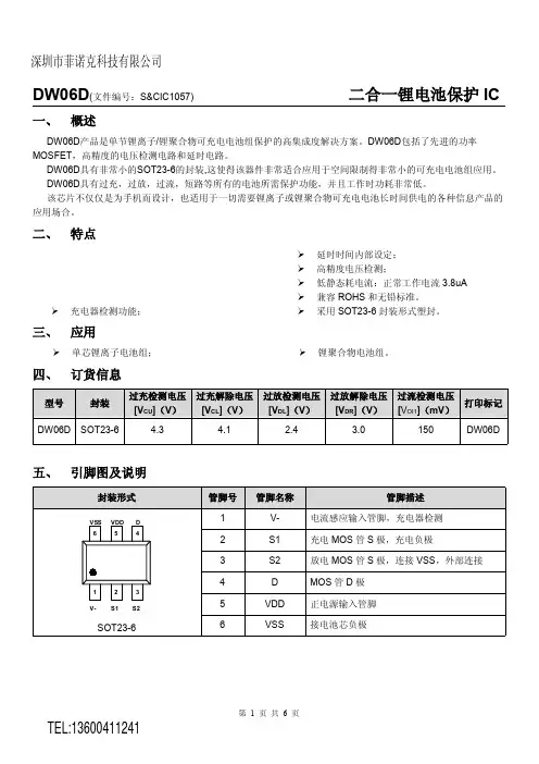
DW06D 二合一锂电池保护IC一、 概述DW06D 产品是单节锂离子/锂聚合物可充电电池组保护的高集成度解决方案。
DW06D 包括了先进的功率MOSFET ,高精度的电压检测电路和延时电路。
DW06D 具有非常小的SOT23-6的封装,这使得该器件非常适合应用于空间限制得非常小的可充电电池组应用。
DW06D 具有过充,过放,过流,短路等所有的电池所需保护功能,并且工作时功耗非常低。
该芯片不仅仅是为手机而设计,也适用于一切需要锂离子或锂聚合物可充电电池长时间供电的各种信息产品的应用场合。
二、 特点内部集成等效50mΩ左右的先进的功率MOSFET ; 过充电流保护;3段过流保护:过放电流1、过放电流2(可选)、负载短路电流; 充电器检测功能;延时时间内部设定; 高精度电压检测;低静态耗电流:正常工作电流3.8uA 兼容ROHS 和无铅标准。
采用SOT23-6封装形式塑封。
三、 应用单芯锂离子电池组;锂聚合物电池组。
四、 订货信息型号封装过充检测电压 [V CU ](V ) 过充解除电压 [V CL ](V ) 过放检测电压 [V DL ](V ) 过放解除电压 [V DR ](V ) 过流检测电流[I OV1](A )打印标记DW06D SOT23-6 4.34.12.43.02.5DW06D五、 引脚图及说明DW06D二合一锂电池保护IC六、极限参数参数符号参数范围单位电源电压VDD VSS-0.3~VSS+12 V CSI输入管脚电压VCSI VDD+15~VDD+0.3 V 工作温度Topr -40~+85 ℃存储温度Tstg -40~+125 ℃七、电气特性参数参数符号测试条件最小值典型值最大值单位工作电压工作电压VDD -- 1.5 -- 10 V 电流消耗工作电流IDD VDD=3.9V -- 3.0 6.0 uA 检测电压过充电检测电压VOCD -- 4.25 4.30 4.35 V 过充电释放电压VOCR -- 4.05 4.10 4.15 V 过放电检测电压VODL -- 2.30 2.40 2.50 V 过放电释放电压VODR -- 2.90 3.00 3.10 V 过电流1检测电压VOI1 -- 0.12 0.15 0.18 V 过电流2(短路电流)检测电压VOI2 VDD=3.6V 0.80 1.00 1.20 V 过电流复位电阻Rshort VDD=3.6V 50 100 150 KΩ过电器检测电压VCH -- -0.8 -0.5 -0.2 V 迟延时间过充电检测迟延时间TOC VDD=3.6V~4.4V -- 110 200 ms 过放电检测迟延时间TOD VDD=3.6V~2.0V -- 80 140 ms 过电流1检测迟延时间TOI1 VDD=3.6V 5 13 20 ms 过电流2(短路电流)检测迟延时间TOI2 VDD=3.6V -- 5 50 us 其他单个MOS管漏极到源极的导通阻抗R DS(on) V GS = 2.5V, I D = 3.3A -- 22.0 30.0 mΩR DS(on) V GS = 4.5V, I D = 8.2A -- 16.0 20.0八、功能描述DW06D监控电池的电压和电流,并通过断开充电器或负载,保护单节可充电锂电池不会因为过充电压,过放电压,过放电流以及短路等情况而损坏。
DW02D (文件编号:S&CIC0921)
二合一锂电池保护IC
一、概述
DW02D 产品是单节锂离子/锂聚合物可充电电池组保护的高集成度解决方案。
DW02D 包括了先进的功率MOSFET ,高精度的电压检测电路和延时电路。
DW02D 具有非常小的SOT23-6的封装并且只需要一个外部元器件,这使得该器件非常适合应用于空间限制得非常小的可充电电池组应用。
DW02D 具有过充,过放,过流,短路等所有的电池所需保护功能,并且工作时功耗非常低。
该芯片不仅仅是为手机而设计,也适用于一切需要锂离子或锂聚合物可充电电池长时间供电的各种信息产品的应用场合。
二、特点
内部集成等效70mΩ的先进的功率MOSFET ; SOT23-6封装;
只需要一个外部电容; 过充电流保护;
3段过流保护:过放电流1、过放电流2(可选)、负载短路电流;
充电器检测功能; 延时时间内部设定; 高精度电压检测;
低静态耗电流:正常工作5.0uA (典型值);休眠状态不超过0.1uA ;
兼容ROHS 和无铅标准。
封装形式
管脚号管脚名称管脚描述
VC C
GN D
VD D
NC BA T T T EST 1234
5
6
1VCC 内部电路供电端2GND 接地端,接电池芯负极3VDD 正电源供电端4
NC 悬空
5BATT 电池组的负极,内部FET 开关连接到GND 6
TEST
测试端
正常工作模式
如果没有检测到任何异常情况,充电和放电过程都将自由转换。
这种情况称为正常工作模式。
过充电压情况
在正常条件下的充电过程中,当电池电压高于过充检测电压(VCU),并持续时间达到过充电压检测延迟时间(tCU)或更长,DW02D 将控制MOSFET 以停止充电。
这种情况称为过充电压情况。
以下两种情况下,过充电压情况将被释放:
1、当电池电压低于过充解除电压(VCL),DW02D 控制充电的FET 导通,回到正常工作模式下。
2、当连接一个负载并且开始放电,DW02D 控制充电的FET 导通回到正常工作模式下。
解除机制如下:接上负载后放电电流立刻流过充电FET 内部寄生二极管开始放电,BATT-电压升到0.7V ,DW02D 检测到这个电压后,当电池电压等于或低于过充检测电压(VCU),DW02D 立刻恢复到正常工作模式,另外,在接上负载放电时,如果BATT-电压等于或低于过流1检测电压,芯片也不会恢复到正常状态。
注:当电池被充电到超过过充检测电压(VCU)并且电池电压没有降到过充检测电压(VCU)以下,即使加上一个可以导致过流的重载,过流1和过流2都不会工作,除非电池电压跌到过充检测电压(VCU)以下。
但是实际上电池是有内阻的,当电池接上一个重载,电池的电压会立即跌落,这时过流1和过流2就会动作。
短路保护与电池电压无关。
DW02D(文件编号:S&CIC0921)二合一锂电池保护IC
过放电压情况
在正常放电过程中,当电池电压降到过放检测电压(VDL)以下的时候,并持续时间达到过放电压检测延时间(tDL)或更长,DW02D将切断电池和负载的连接,停止放电。
这种情况被称为过放电压情况。
当控制放电的FET 被关断,BATT-通过内部BATT-与VDD之间的RBATT-D电阻被拉到高电平。
当BATT-电压高于负载短路检测电压,芯片的耗电流会降到休眠电流(IPDN)。
这种情况被称为休眠情况。
在过放和休眠情况中BATT-和VDD之间由RBATT-D电阻连接。
当一个充电器连接上并且BATT-和VDD之间电势差变到1.3V(典型值)或更高(负载短路检测电压)时休眠状态解除。
这时放电FET仍然断开。
当电池电压变成过放检测电压(VDL)或更高(见备注),
DW02D使FET导通回到正常工作模式。
.
备注:当过放情况下的电池接上充电器,如果BATT-端电压不低于充电器检测电压(VCHA),并且电池电压达到过放解除电压或更高(VDR)过放情况解除(控制放电的FET导通)。
过放电流情况
正常工作模式下,当放电电流等于或高于设定的值(BATT-电压等于或高于过电流检测电压)并且时间持续超过过电流检测延时时间时,DW02D关断放电FET停止放电。
这个称为过放电流情况(包括过放电流1,过放电流2和负载短路电流)。
过电流情况下BATT-和GND间内部连接了RBATT-S电阻。
当一个负载连接上,BATT-电压等于VDD流过负载电阻后的电压。
根据切断负载等行为,B+和B-之间的阻抗增大至大于等于能够自动恢复到正常状态的阻抗,过放电流状态将被解除,回到正常状态。
由于BATT-和GND之间连接RBATT-S电阻,当负载断开,BATT-电压被拉到地电位。
当侦测到BATT-电位低于过流1检测电压(VIOV1),芯片回到正常状态。
不正常充电电流情况
正常充电时,如果BATT-电压降到充电检测电压以下(VCHA),持续时间超过过充电压检测延时时间(tCU),DW02D关断充电FET停止充电。
这就被称为不正常充电电流检测。
当放电FET导通并且BATT-电压将到充电检测电压(VCHA)以下时不正常充电电流检测工作。
过放电压情况时,当不正常的充电电流流入电池,在电池电压变到过放检测电压并且持续时间达到过充检测电压延迟时间(tCU),DW02D关断充电FET停止充电。
断开充电器,BATT-和GND之间电压低于充电器检测电压(VCHA)时,不正常充电电流模式解除。
由于0V电池充电功能优先级高于不正常电流充电检测,电池电压很低的电池正在进行0V充电时,不正常充电电流检测将不工作。
负载短路情况
如果BATT-电压高于短路保护电压(VSHORT),DW02D将与负载断开停止放电。
延迟时间不超过tSHORT。
当BATT-电压高于短路保护电压(VSHORT)时,例如负载被移除,负载短路情况将解除。
延时电路
当过放电流1被检测到,过放电流2和负载短路的检测延时时间就开始计算。
一旦测到过放电电流2或者负载短路的时间超过过放电电流2或负载短路的延迟时间,DW02D将停止放电。
当检测出过放电流,且超出过放检测延迟时间,这时若电池电压低于过放检测电压,系统将进入休眠状态。
若因为过放电流,过放电压降至过放检测电压,DW02D将通过过放电流检测停止放电。
这种情况下,电池电压的恢复非常慢,如果在过放电压检测延迟时间之后,电池电压仍然低于过放检测,DW02D将转至休眠情况。
DW02D(文件编号:S&CIC0921)二合一锂电池保护IC 2、过放电流检测
备注:(1)正常工作状态(2)过充电压状态(3)过放电压状态(4)过流状态
3、充电器检测
DW02D(文件编号:S&CIC0921)二合一锂电池保护IC 4、不正常充电电流检测
备注:(1)正常工作状态(2)过充电压状态(3)过放电压状态(4)过电流状态
十一、典型特性
(除非特别指出V BA T=3.6V,T A=25℃)
DW02D(文件编号:S&CIC0921)二合一锂电池保护IC。